EP0083991A2 - Matériau pour l'enregistrement d'informations par voie optique - Google Patents
Matériau pour l'enregistrement d'informations par voie optique Download PDFInfo
- Publication number
- EP0083991A2 EP0083991A2 EP83300121A EP83300121A EP0083991A2 EP 0083991 A2 EP0083991 A2 EP 0083991A2 EP 83300121 A EP83300121 A EP 83300121A EP 83300121 A EP83300121 A EP 83300121A EP 0083991 A2 EP0083991 A2 EP 0083991A2
- Authority
- EP
- European Patent Office
- Prior art keywords
- recording medium
- recording
- layer
- protective coating
- recording material
- Prior art date
- Legal status (The legal status is an assumption and is not a legal conclusion. Google has not performed a legal analysis and makes no representation as to the accuracy of the status listed.)
- Withdrawn
Links
Images

Classifications
-
- G—PHYSICS
- G11—INFORMATION STORAGE
- G11B—INFORMATION STORAGE BASED ON RELATIVE MOVEMENT BETWEEN RECORD CARRIER AND TRANSDUCER
- G11B7/00—Recording or reproducing by optical means, e.g. recording using a thermal beam of optical radiation by modifying optical properties or the physical structure, reproducing using an optical beam at lower power by sensing optical properties; Record carriers therefor
- G11B7/24—Record carriers characterised by shape, structure or physical properties, or by the selection of the material
- G11B7/241—Record carriers characterised by shape, structure or physical properties, or by the selection of the material characterised by the selection of the material
- G11B7/252—Record carriers characterised by shape, structure or physical properties, or by the selection of the material characterised by the selection of the material of layers other than recording layers
- G11B7/254—Record carriers characterised by shape, structure or physical properties, or by the selection of the material characterised by the selection of the material of layers other than recording layers of protective topcoat layers
- G11B7/2542—Record carriers characterised by shape, structure or physical properties, or by the selection of the material characterised by the selection of the material of layers other than recording layers of protective topcoat layers consisting essentially of organic resins
-
- G—PHYSICS
- G11—INFORMATION STORAGE
- G11B—INFORMATION STORAGE BASED ON RELATIVE MOVEMENT BETWEEN RECORD CARRIER AND TRANSDUCER
- G11B7/00—Recording or reproducing by optical means, e.g. recording using a thermal beam of optical radiation by modifying optical properties or the physical structure, reproducing using an optical beam at lower power by sensing optical properties; Record carriers therefor
- G11B7/24—Record carriers characterised by shape, structure or physical properties, or by the selection of the material
- G11B7/241—Record carriers characterised by shape, structure or physical properties, or by the selection of the material characterised by the selection of the material
- G11B7/242—Record carriers characterised by shape, structure or physical properties, or by the selection of the material characterised by the selection of the material of recording layers
- G11B7/243—Record carriers characterised by shape, structure or physical properties, or by the selection of the material characterised by the selection of the material of recording layers comprising inorganic materials only, e.g. ablative layers
- G11B2007/24302—Metals or metalloids
- G11B2007/2431—Metals or metalloids group 13 elements (B, Al, Ga, In)
-
- G—PHYSICS
- G11—INFORMATION STORAGE
- G11B—INFORMATION STORAGE BASED ON RELATIVE MOVEMENT BETWEEN RECORD CARRIER AND TRANSDUCER
- G11B7/00—Recording or reproducing by optical means, e.g. recording using a thermal beam of optical radiation by modifying optical properties or the physical structure, reproducing using an optical beam at lower power by sensing optical properties; Record carriers therefor
- G11B7/24—Record carriers characterised by shape, structure or physical properties, or by the selection of the material
- G11B7/241—Record carriers characterised by shape, structure or physical properties, or by the selection of the material characterised by the selection of the material
- G11B7/242—Record carriers characterised by shape, structure or physical properties, or by the selection of the material characterised by the selection of the material of recording layers
- G11B7/243—Record carriers characterised by shape, structure or physical properties, or by the selection of the material characterised by the selection of the material of recording layers comprising inorganic materials only, e.g. ablative layers
- G11B2007/24302—Metals or metalloids
- G11B2007/24314—Metals or metalloids group 15 elements (e.g. Sb, Bi)
-
- G—PHYSICS
- G11—INFORMATION STORAGE
- G11B—INFORMATION STORAGE BASED ON RELATIVE MOVEMENT BETWEEN RECORD CARRIER AND TRANSDUCER
- G11B7/00—Recording or reproducing by optical means, e.g. recording using a thermal beam of optical radiation by modifying optical properties or the physical structure, reproducing using an optical beam at lower power by sensing optical properties; Record carriers therefor
- G11B7/24—Record carriers characterised by shape, structure or physical properties, or by the selection of the material
- G11B7/241—Record carriers characterised by shape, structure or physical properties, or by the selection of the material characterised by the selection of the material
- G11B7/242—Record carriers characterised by shape, structure or physical properties, or by the selection of the material characterised by the selection of the material of recording layers
- G11B7/243—Record carriers characterised by shape, structure or physical properties, or by the selection of the material characterised by the selection of the material of recording layers comprising inorganic materials only, e.g. ablative layers
- G11B2007/24302—Metals or metalloids
- G11B2007/24316—Metals or metalloids group 16 elements (i.e. chalcogenides, Se, Te)
-
- G—PHYSICS
- G11—INFORMATION STORAGE
- G11B—INFORMATION STORAGE BASED ON RELATIVE MOVEMENT BETWEEN RECORD CARRIER AND TRANSDUCER
- G11B7/00—Recording or reproducing by optical means, e.g. recording using a thermal beam of optical radiation by modifying optical properties or the physical structure, reproducing using an optical beam at lower power by sensing optical properties; Record carriers therefor
- G11B7/24—Record carriers characterised by shape, structure or physical properties, or by the selection of the material
- G11B7/241—Record carriers characterised by shape, structure or physical properties, or by the selection of the material characterised by the selection of the material
- G11B7/252—Record carriers characterised by shape, structure or physical properties, or by the selection of the material characterised by the selection of the material of layers other than recording layers
-
- G—PHYSICS
- G11—INFORMATION STORAGE
- G11B—INFORMATION STORAGE BASED ON RELATIVE MOVEMENT BETWEEN RECORD CARRIER AND TRANSDUCER
- G11B7/00—Recording or reproducing by optical means, e.g. recording using a thermal beam of optical radiation by modifying optical properties or the physical structure, reproducing using an optical beam at lower power by sensing optical properties; Record carriers therefor
- G11B7/24—Record carriers characterised by shape, structure or physical properties, or by the selection of the material
- G11B7/241—Record carriers characterised by shape, structure or physical properties, or by the selection of the material characterised by the selection of the material
- G11B7/252—Record carriers characterised by shape, structure or physical properties, or by the selection of the material characterised by the selection of the material of layers other than recording layers
- G11B7/257—Record carriers characterised by shape, structure or physical properties, or by the selection of the material characterised by the selection of the material of layers other than recording layers of layers having properties involved in recording or reproduction, e.g. optical interference layers or sensitising layers or dielectric layers, which are protecting the recording layers
- G11B7/2572—Record carriers characterised by shape, structure or physical properties, or by the selection of the material characterised by the selection of the material of layers other than recording layers of layers having properties involved in recording or reproduction, e.g. optical interference layers or sensitising layers or dielectric layers, which are protecting the recording layers consisting essentially of organic materials
Definitions
- the present invention relates to an optical type recording medium. More specifically, it relates to an optical type recording medium suitable for use in an optical disc having improved water-vapor resistance which does not impair the recording sensitivity of a recording material layer.
- information is recorded in a recording layer composed of a low melting point metal formed on the surface of a substrate by irradiating a strong photobeam on the recording layer to open information holes (i.e. pits) as a result of the melting of the metal by the heat caused by the photobeam.
- the recorded information is read out (or detected), based on the presence or absence of pits in the recording layer, by irradiating a weak photobeam on the recording layer.
- the reading can be effected by detecting the difference in the amount of the light reflected by the irradiated photobeam from the pit portions and the non-pit portions.
- the photobeams striking the non-pit portions are reflected at a relatively high reflectance due to the metallic luster of the metallic layer, whereas the photobeams striking the pit portions pass through the pit portions at a relatively high transmittance.
- optical devices have a high recording capacity, i.e., about one hundred times of that of commercially available magnetic discs, and are also optimum for use in the image treating and office automation fields from the viewpoint of the cost.
- the known recording media for use in optical discs comprise, for example, a thin film of a recording material such as bismuth (Bi) or tellurium (Te) formed as a recording material layer on the surface of a substrate by, for example, a standard vapor deposition technique.
- a recording material such as bismuth (Bi) or tellurium (Te) formed as a recording material layer on the surface of a substrate by, for example, a standard vapor deposition technique.
- the recording materials should be heat meltable and should desirably have good chemical and physical stability and good water-vapor resistance.
- Water-vapor resistance is a very important property of recording materials from the viewpoint of the improvement in the reliability of the recording medium. For instance, in the case of a tellurium recording material, the recording material per se will oxidize in the presence of water vapor to form a light (or radiation) transmissible oxide. This prevents the reading of the recorded information since the transparent non-pit portions then allow the reading photobeams to pass therethrough as the pit portions.
- the use of the polymer materials is disadvantageous due to increased production cost, since the polymer material layer cannot be formed by a vapour deposition technique as used in the formation of the recording layer. Furthermore, polymer materials suffer from carbonation due to the heat caused during the recording of information, thereby preventing formation of pits having smooth and regular profiles.
- An optical type information recording medium is suitable for writing information by irradiating a photobeam on a recording material layer to cause a physical change in the recording material layer and comprises a substrate, the recording material layer formed on the substrate and a protective coating layer formed on at least the surface of the recording material layer opposite to the substrate and is characterised in that the protective coating layer is formed of a porphyrin type compound.
- the protective coating layer By using a porphyrin type compound as the protective coating layer it is possible to provide a coating that imparts improved water-vapour resistance and which does not impair the recording sensitivity. Another advantage is that it is possible to form this protective coating layer in the same process as that in which the recording material layer is formed.
- the amount of porphyrin type compound must be sufficient to impart the desired protective properties.
- the thickness of the coating is generally at least 5 nm.
- the coating is generally formed substantially only of the porphyrin type compound.
- the porphyrin type compound is a compound having the characteristic cyclic structure of porphine and includes the compounds in which the methine bridges of porphine are replaced by nitrogen.
- the compounds include tetrabenztetrazaporphines, such as various metal phthalocyanines, and these are preferred for use in the invention.
- an optical type information recording medium 10 comprises a radiation (or light) transmissible substrate 11, a recording material layer 12, and a protective coating layer 13.
- an optical type information recording medium 20 comprises a radiation transmissible substrate 21, a radiation transmissible subbing layer 22, a sublimable organic substance layer 23, a recording material layer 24 and a protective coating layer 25.
- optical type information recording media can be assembled as a so-called air sandwich type optical disc 30 as shown in Fig. 3.
- the optical disc 30 comprises radiation transmissible substrates 31, recording layers 32, and spacers 34, and protective coating layers (not shown).
- Reference numeral 33 represents an air layer enclosed by the substrates 31 and spacers 34.
- the radiation transmissible (or transparent) substrates 21 can be formed by any radiation transmissible synthetic resin, such as poly(methyl methacrylate), polycarbonate, poly(vinyl chloride), and polystyrene as well as glass.
- synthetic resin such as poly(methyl methacrylate), polycarbonate, poly(vinyl chloride), and polystyrene as well as glass.
- the use of synthetic resin is advantageous over glass due to synthetic resin's smaller thermal conductivity and, therefore, higher recording sensitivity.
- the radiation transmissible (or transparent) subbing layer 22 can be composed of any radiation transmissible inorganic materials having a melting point higher than that of the material of the recording layer 23. Typical examples of such inorganic materials are SiO 2 , MgF 2 , and A1 2 0 3 .
- the radiation transmissible subbing layer 22 can be readily formed on the surface of the substrate 21 by any known vapor deposition technique. Although there is no limitation on the thickness of the subbing layer 22, the thickness is generally 3 nm or more, desirably 5 to 15 nm.
- the use of the subbing layer 22 in the recording media 20 results in a high signal-to-noise ratio in the reproduction signal. This is disclosed in detail in our Japanese Patent Application No. 56-207862 filed on December 22, 1981. This subbing layer also act as a protective layer for the recording material layer from the side of the substrate.
- the sublimable organic substance layer 23 can be composed of any sublimable organic substance having a sublimation point not far from the melting point of the material forming the recording material layer 24.
- Typical examples of such organic substances are copper phthalocianine, having a sublimation point of 420°C to 430°C, fluorescein, having a sublimation point of 314°C to 316°C, and lead phthalocianine, having a sublimation point of 450°C to 500°C.
- the sublimable organic substance layer 23 can be readily, formed on the subbing layer 22 by any known vapor deposition technique. Although there is no limitation on the thickness of the organic substance layer 23, the thickness is generally 5 nm or more, desirably 10 to 100 nm.
- the use of the organic layer 23 assists the smooth melting and hole-opening of the recording material layer 24 when information is written in the recording layer by irradiating a photobeam on the recording layer.
- a metal layer composed of, for example, Te, Bi, In, Se, As, Pb, or Sn, or alloys obtained therefrom, can be placed between the subbing layer 22 and the sublimable organic substance layer 23 as disclosed in the above-mentioned Japanese Patent Application.
- Use of the metal layer improves the photosensitivity of the recording medium when information is recorded and also results in a better S/N ratio when the recorded information is reproduced.
- the recording material layers 12 and 24 can be composed of any conventional recording materials such as metals having a relatively low melting point (e.g., about 1000°C or less) and a relatively low thermal conductivity (e.g., 0.1 cal/sec ⁇ cm ⁇ deg or less).
- metals having a relatively low melting point (e.g., about 1000°C or less) and a relatively low thermal conductivity (e.g., 0.1 cal/sec ⁇ cm ⁇ deg or less).
- Typical examples of such metals are Te (m.p. 450°C), Bi (m.p. 271°C), In (m.p. 157°C), Se (m.p. 221°C), As (m.p. 6l2°C), Pb (m.p. 327°C), and Sn (m.p. 232°C). Any alloys obtained therefrom and any mixture thereof can also be used.
- the recording material layers 12 and 24 can be readily formed on the substrate 11 and the organic substance layer 23, respectively, by any known vapor deposition technique. Although there is no limitation on the thickness of the recording material layers 12 and 24, the thickness is generally 5 nm or more, desirably 10 to 100 nm. Use of a recording material layer 12 and 24 having too large a thickness necessitates a large amount of light energy for melting the metal to open pits.
- the protective coating layers 13 and 25, essentially composed of a porphyrin type compound are formed or laminated on the recording material layers 12 and 24 to protect the recording media 10 and 20 from water vapor.
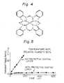
- Typical examples of such porphyrin type compounds usable in the present invention are copper phthalocianine having the chemical formula as illustrated in Fig. 4, lead phthalocianine, cobalt phthalocianine, iron phthalocianine, vanadium phthalocianine, or any mixture thereof.
- the protective coating layers 12 and 24 can be readily formed on the recording material layers 12 and 24, respectively, by any known vapor deposition technique.
- the thickness of the protective coating layers 12 and 24 is generally 5 nm or more, desirably 10 to 100 nm.
- Use of a protective coating layer having too large a thickness tends to decrease the recording sensitivity of the information recording medium. Contrary to this, use of a protective coating layer having too small a thickness does not achieve the desired purpose.
- the protective coating layer can also be formed, for example, between the substrate 11 and the recording material layer 12 or on any position between the substrate 21 and the recording material layer 24, in addition to the protective coating layers 13 and 25.
- a porphyrin type compound as a protective layer on the recording material layer formed on the substrate prevents oxidation of the information recording material due to presence of water vapor without causing any substantial decrease in the sensitivity of the information recording material.
- the protective coating layer can be formed in the same process for producing the recording material layer.
- a glass substrate having a diameter of 300 mm and having a thickness of 1.0 mm was placed, after washing, in a bell-jar.
- Te having a melting point of 450°C in a boat located in the bell-jar was heated under a pressure of 10 -6 Torr, while the deposited substrate was turned at a speed of 1 to 2 rpm, to deposit a Te layer having a thickness of 30 nm on the surface of the substrate.
- copper phthalocianine having a melting point of 430°C in a boat located in the bell-jar was heated under a pressure of 10 -6 Torr, while the deposited substrate was turned at a speed of 1 to 2 rpm, to deposit a copper phthalicianine coating layer having a thickness of 30 nm on the Te layer.
- a Te layer having a thickness of 30 nm was deposited on the surface of the glass substrate used above in the same manner as in Example 1. Then, a SiO 2 layer having a thickness of 30 nm was deposited on the Te layer by heating SiO 2 in a boat located in the bell jar under a pressure of 10-6 Torr, while the deposited substrate was turned at a speed of 1 to 2 rpm.
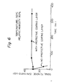
- the water vapor resistance of the information recording media thus obtained was determined under the conditions of a temperature of 60°C and a relative humidity of 90% after recording the predetermined information. The results are shown in Table 1 and Figs. 5 and 6.
- FIG. 5 shows the changes in the transmittance ratios (i.e., the transmittance T after humidity test/the initial transmittance To) of the recording media of Example 1 (with protective coating layer) and Comparative Example 1 (with no protective coating layer) with the lapse of time.
- the transmittance ratio of Example 1 slightly changed between 0 and about 100 hours. Thereafter, no substantial change in the transmittance ratio (T/To) was observed. Contrary to this, the transmittance ratio of the recording medium of Comparative Example 1 with no protective coating layer remarkably increased with the lapse of time.
- the increase in the transmittance ratio means the progressive oxidation of the Te layer with the lapse of time due to the presence of water vapor.
- the temperature of 60°C and a relative humidity of 90% are accelerated test conditions.
- the above-mentioned results of Example 1 the present recording medium can be used for 10 years or more under ordinary conditions.
- Figure 6 shows the changes in the signal to noise ratio (S/N) (i.e., the quality) of the recording media of Example 1 (with protective coating layer) and Comparative Example 1 (with no protective coating layer) with the lapse of time.
- S/N signal to noise ratio
- a poly(methyl methacrytate) substrate having a diameter of 300 mm and having a thickness of 1.2 mm was placed, after washing, in a bell-jar.
- SiO in a boat located in the bell--jar was heated under a pressure of 10 -6 Torr, while the substrate was turned at a speed of 120 rpm, to deposit a SiO layer having a thickness of 10 nm on the surface of the substrate.
- Example 3 an information recording medium was prepared in the same manner as in Example 2, except that no top copper phthalocianine protective coating layer was deposited on the Te layer..
Landscapes
- Optical Record Carriers And Manufacture Thereof (AREA)
- Thermal Transfer Or Thermal Recording In General (AREA)
Applications Claiming Priority (2)
| Application Number | Priority Date | Filing Date | Title |
|---|---|---|---|
| JP3837/82 | 1982-01-13 | ||
| JP57003837A JPS58121153A (ja) | 1982-01-13 | 1982-01-13 | 光学式情報媒体 |
Publications (2)
| Publication Number | Publication Date |
|---|---|
| EP0083991A2 true EP0083991A2 (fr) | 1983-07-20 |
| EP0083991A3 EP0083991A3 (en) | 1984-02-08 |
Family
ID=11568290
Family Applications (1)
| Application Number | Title | Priority Date | Filing Date |
|---|---|---|---|
| EP83300121A Withdrawn EP0083991A3 (en) | 1982-01-13 | 1983-01-11 | Optical type information recording medium |
Country Status (2)
| Country | Link |
|---|---|
| EP (1) | EP0083991A3 (fr) |
| JP (1) | JPS58121153A (fr) |
Cited By (8)
| Publication number | Priority date | Publication date | Assignee | Title |
|---|---|---|---|---|
| EP0143992A1 (fr) * | 1983-11-02 | 1985-06-12 | Ricoh Company, Ltd | Milieu d'enregistrement optique d'information |
| WO1986000575A1 (fr) * | 1984-07-16 | 1986-01-30 | Minnesota Mining And Manufacturing Company | Constructions de formation d'images d'arts graphiques utilisant des couches a deposition de vapeur |
| US4719170A (en) * | 1985-03-02 | 1988-01-12 | Basf Aktiengesellshaft | Optical recording material |
| EP0317696A1 (fr) * | 1987-11-23 | 1989-05-31 | Taiyo Yuden Co., Ltd. | Milieu d'enregistrement d'information optique |
| EP0259151A3 (en) * | 1986-09-03 | 1989-09-13 | Canon Kabushiki Kaisha | Optical card and process for producing it |
| EP0408271A3 (en) * | 1989-07-10 | 1991-11-13 | Sanyo Electric Co., Ltd. | Optical memory medium |
| US5248584A (en) * | 1986-09-03 | 1993-09-28 | Canon Kabushiki Kaisha | Optical card and method for reading information recorded in it |
| US11999928B2 (en) | 2009-11-13 | 2024-06-04 | Novozymes A/S | Brewing method |
Families Citing this family (2)
| Publication number | Priority date | Publication date | Assignee | Title |
|---|---|---|---|---|
| JPS6074135A (ja) * | 1983-09-29 | 1985-04-26 | Nippon Columbia Co Ltd | 光情報記録媒体 |
| JPS62266748A (ja) * | 1986-05-02 | 1987-11-19 | ドレクスラ−・テクノロジイ・コ−ポレ−シヨン | 光学デ−タ記憶媒体 |
Family Cites Families (4)
| Publication number | Priority date | Publication date | Assignee | Title |
|---|---|---|---|---|
| NL7900281A (nl) * | 1979-01-15 | 1980-07-17 | Philips Nv | Optische registratie-inrichting alsmede een werkwijze voor het registreren van informatie langs optische weg. |
| GB2066489B (en) * | 1979-11-29 | 1983-10-19 | Rca Corp | Ablative optical recording medium |
| JPS6023038B2 (ja) * | 1980-04-30 | 1985-06-05 | 富士通株式会社 | 光学記録用媒体 |
| JPS57151397A (en) * | 1981-03-17 | 1982-09-18 | Ricoh Co Ltd | Optical information recording medium |
-
1982
- 1982-01-13 JP JP57003837A patent/JPS58121153A/ja active Pending
-
1983
- 1983-01-11 EP EP83300121A patent/EP0083991A3/en not_active Withdrawn
Cited By (10)
| Publication number | Priority date | Publication date | Assignee | Title |
|---|---|---|---|---|
| EP0143992A1 (fr) * | 1983-11-02 | 1985-06-12 | Ricoh Company, Ltd | Milieu d'enregistrement optique d'information |
| US4752554A (en) * | 1983-11-02 | 1988-06-21 | Ricoh Co., Ltd. | Optical information recording medium |
| WO1986000575A1 (fr) * | 1984-07-16 | 1986-01-30 | Minnesota Mining And Manufacturing Company | Constructions de formation d'images d'arts graphiques utilisant des couches a deposition de vapeur |
| US4719170A (en) * | 1985-03-02 | 1988-01-12 | Basf Aktiengesellshaft | Optical recording material |
| EP0259151A3 (en) * | 1986-09-03 | 1989-09-13 | Canon Kabushiki Kaisha | Optical card and process for producing it |
| US5248584A (en) * | 1986-09-03 | 1993-09-28 | Canon Kabushiki Kaisha | Optical card and method for reading information recorded in it |
| EP0317696A1 (fr) * | 1987-11-23 | 1989-05-31 | Taiyo Yuden Co., Ltd. | Milieu d'enregistrement d'information optique |
| US4920359A (en) * | 1987-11-23 | 1990-04-24 | Taiyo Yuden Co., Ltd. | Optical information recording medium having protective layer |
| EP0408271A3 (en) * | 1989-07-10 | 1991-11-13 | Sanyo Electric Co., Ltd. | Optical memory medium |
| US11999928B2 (en) | 2009-11-13 | 2024-06-04 | Novozymes A/S | Brewing method |
Also Published As
| Publication number | Publication date |
|---|---|
| EP0083991A3 (en) | 1984-02-08 |
| JPS58121153A (ja) | 1983-07-19 |
Similar Documents
| Publication | Publication Date | Title |
|---|---|---|
| EP0084729A1 (fr) | Elements d'enregistrement | |
| US4670345A (en) | Information recording medium | |
| US5252370A (en) | Optical recording medium and method for making | |
| EP0135370A1 (fr) | Elément pour enregistrer une information | |
| JPH0415112B2 (fr) | ||
| EP0097929B1 (fr) | Milieu enregistreur optique d'information pour laser semi-conducteur | |
| US5334433A (en) | Optical recording medium | |
| EP0083991A2 (fr) | Matériau pour l'enregistrement d'informations par voie optique | |
| EP0376231B1 (fr) | Support d'enregistrement optique | |
| EP1310953B1 (fr) | Elément d' enregistrement à base de changement de phase pour l' application à l' écriture unique | |
| JPH0725200B2 (ja) | 情報の記録媒体 | |
| JPH0380635B2 (fr) | ||
| JP4778300B2 (ja) | 追記型光記録媒体 | |
| JPH042436B2 (fr) | ||
| JPH0447909B2 (fr) | ||
| JPS62125552A (ja) | 光記録媒体 | |
| KR950003183B1 (ko) | 광자기 기록매체 | |
| JPH042437B2 (fr) | ||
| JPS61229242A (ja) | 光学的情報記録再生方法 | |
| JPH0251391B2 (fr) | ||
| JPH04178934A (ja) | 光記録媒体の製造方法 | |
| JPH05262040A (ja) | 光情報記録媒体 | |
| JPS58185295A (ja) | 光記録媒体 | |
| JPH0250874B2 (fr) | ||
| JPS59131493A (ja) | 光学記録媒体の製造方法 |
Legal Events
| Date | Code | Title | Description |
|---|---|---|---|
| PUAI | Public reference made under article 153(3) epc to a published international application that has entered the european phase |
Free format text: ORIGINAL CODE: 0009012 |
|
| AK | Designated contracting states |
Designated state(s): DE FR GB NL |
|
| PUAL | Search report despatched |
Free format text: ORIGINAL CODE: 0009013 |
|
| AK | Designated contracting states |
Designated state(s): DE FR GB NL |
|
| 17P | Request for examination filed |
Effective date: 19840724 |
|
| STAA | Information on the status of an ep patent application or granted ep patent |
Free format text: STATUS: THE APPLICATION IS DEEMED TO BE WITHDRAWN |
|
| 18D | Application deemed to be withdrawn |
Effective date: 19851217 |
|
| RIN1 | Information on inventor provided before grant (corrected) |
Inventor name: OGAWA, SEIYO Inventor name: GOTO, HIRONORI Inventor name: GOTO, YASUYUKI Inventor name: KOSHINO, NAGAAKI Inventor name: OGAWA, KOICHINICHIMO HIYOSHI DAI-3 |