EP0084252B1 - Dispositif de mémoire à semi-conducteurs - Google Patents
Dispositif de mémoire à semi-conducteurs Download PDFInfo
- Publication number
- EP0084252B1 EP0084252B1 EP82306888A EP82306888A EP0084252B1 EP 0084252 B1 EP0084252 B1 EP 0084252B1 EP 82306888 A EP82306888 A EP 82306888A EP 82306888 A EP82306888 A EP 82306888A EP 0084252 B1 EP0084252 B1 EP 0084252B1
- Authority
- EP
- European Patent Office
- Prior art keywords
- voltage
- schottky barrier
- diode
- current
- transistor
- Prior art date
- Legal status (The legal status is an assumption and is not a legal conclusion. Google has not performed a legal analysis and makes no representation as to the accuracy of the status listed.)
- Expired
Links
Images


Classifications
-
- G—PHYSICS
- G11—INFORMATION STORAGE
- G11C—STATIC STORES
- G11C11/00—Digital stores characterised by the use of particular electric or magnetic storage elements; Storage elements therefor
- G11C11/21—Digital stores characterised by the use of particular electric or magnetic storage elements; Storage elements therefor using electric elements
- G11C11/34—Digital stores characterised by the use of particular electric or magnetic storage elements; Storage elements therefor using electric elements using semiconductor devices
- G11C11/40—Digital stores characterised by the use of particular electric or magnetic storage elements; Storage elements therefor using electric elements using semiconductor devices using transistors
- G11C11/41—Digital stores characterised by the use of particular electric or magnetic storage elements; Storage elements therefor using electric elements using semiconductor devices using transistors forming static cells with positive feedback, i.e. cells not needing refreshing or charge regeneration, e.g. bistable multivibrator or Schmitt trigger
- G11C11/413—Auxiliary circuits, e.g. for addressing, decoding, driving, writing, sensing, timing or power reduction
- G11C11/414—Auxiliary circuits, e.g. for addressing, decoding, driving, writing, sensing, timing or power reduction for memory cells of the bipolar type
- G11C11/415—Address circuits
Definitions
- the present invention relates to a semiconductor memory device, more particularly to a semiconductor memory device comprised of static type memory cells each including, as a load, two parallel circuits each comprised of both a Schottky barrier diode (SBD) and resistor.
- SBD Schottky barrier diode
- a static type memory cell is usually comprised of a pair of transistors formed as a flip-flop and of loads connected to these transistors.
- the memory cell is driven by a word line and a bit line.
- the word line is driven by a socalled word decoder driver and the bit line is driven by a bit current supplying circuit (explained in detail hereinafter).
- the loads to be connected to the transistors usually comprise a resistor.
- loads have often been constructed in a form of SBD's and resistors in parallel circuits. Such loads have the advantage of enabling a high degree of speed in the read/write operation in the memory. The reason for this is well known.
- a prior art semiconductor memory device having the features of the pre-characterising part of claim 1 is disclosed herein and shown in Fig. 1.
- Japanese patent application 56-159894 discloses a memory device having memory cells which include load diodes (which are not disclosed to be Schottky barrier diodes).
- a circuit for controlling read and write incorporates reference voltage generating circuits comprising diodes of the same form as load diodes of a memory cell disposed on both sides of the memory cell. If diode characteristics of the load diodes fluctuate, the characteristics of the diodes in the reference voltage generating circuits vary in a similar manner.
- U.S. Patent No. 4 057 789 discloses a memory device in which memory cells comprise loads in the form of a Schottky barrier diode and a resistor in parallel.
- a sense amplifier of the device employs a reference voltage source and a "simulated memory cell".
- the "simulated memory cell” incorporates a Schottky barrier diode, and is provided for simulating the loading of a number of memory cells as seen by a word driver.
- the currents flowing in the reference voltage source simulate currents flowing in the memory cells, so that when potentials in the memory cells change with temperature, potentials in the bias circuit change in a related manner.
- the output potential of the reference voltage source is thus maintained at a mid value of the voltage swing of the memory cells.
- a semiconductor memory device comprising:
- An embodiment of the present invention can provide a semiconductor memory device in which a bias circuit works not only to achieve its inherent biasing operation, but also to easily suppress the effect of variation of V F to substantially zero, thereby eliminating the above two problems of the prior art.
- a bias circuit incorporates an SBD identical to SBD's comprised in the memory cell, in consideration of the experimentally proved fact that all SBD's produced from the same production lot have substantially the same value of V F . Consequently, when the V F of the SBD is large, it will increase the current flowing through a first constantcurrent circuit, (mentioned later), thereby decreasing the "low level" of the word line, and, simultaneously, increase the current flowing through a second constantcurrent circuit, (mentioned later).
- Figure 1 is a circuit diagram of a prior art semiconductor memory device.
- reference numeral 11 represents one of the static type memory cells; in actuality, many identical memory cells (not shown) are arranged in both the X and Y directions.
- the memory cell 11 is connected to both word line 12 and bit lines, i.e. bit line pair, 13.
- word line 12 and bit lines i.e. bit line pair, 13.
- bit line pair i.e. bit line pair
- the word line 12 is connected to a word decoder driver 14 provided with a first constant- current circuit 18.
- Reference numeral 16 represents a word driver.
- Reference numeral 17 represents a group of diodes which cooperate with the first constant-current circuit 18 so as to construct a word decoder of the diode-matrix type.
- Reference symbol AD denotes an address.
- the bit lines 13 are connected to a second constantcurrent circuit 15 so as to produce bit currents flowing through the bit-lines.
- the second constant-current circuit 15 is connected to a bias circuit 19 together with the first constant-current circuit 18. (Alternatively, the circuit 15 may be connected independently from the circuit 18). This bias circuit 19 functions to maintain the constant currents flowing through the circuits 15 and 18 at predetermined values.
- the present invention particularly refers to a static type memory cell including an SBD therein.
- the loads to be connected to transistors Q, and Q 2 comprising the memory cell 11 in a form of a flip-flop, are constructed as a first parallel circuit of an SBD D S1 and a resistor R, and a second parallel circuit of an SBD D S2 and a resistor R 2 , respectively.
- a hold current IH is absorbed from the memory cell via the transistors Q, and Q 2 .
- the merit of utilizing the SBD's resides in, as previously mentioned, achieving high speed read/write operation of the memory.
- the SBD is not advantageous from the viewpoint of the forward voltage V F . That is, as previously mentioned, the voltage V F is not constant but varies due to the manufacturing process.
- the variation of the V F defined by the SBD's D S1 and D s2 causes variation in the "low" level of a nonselected word line. If the memory cell 11 is connected to the currently nonselected word line the variation of the V F will swing the "low" level of the word line 12, determined by the emitter voltage of the word driver 16, upward or downward.
- Such variation of the word line voltage will often produce erroneous write operations. Therefore, a large write margin must usually be taken into consideration during the write operation to substantially absorb such variation.
- a large V F may sometimes causes a write current to be divided (diverted) into the transistor Q 1 , or Q 2 which is off during the write operation. Such division of the write current into an off transistor will lead to insufficient write current for achieving the optimal write operation. Therefore, it is necessary to compensate for such insufficiency of the write current due to division of the write current.
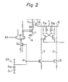
- FIG. 2 is a circuit diagram of semiconductor memory device according to a first embodiment of the present invention.
- members the same as those of Fig. 1 are represented by the same reference numerals or symbols. (Same for later Figures).
- reference numeral 20 represents a bias circuit, in the bias circuit 20, an SBD D 53 is incorporated.
- the V F characteristic of the SBD Dg 3 is substantially the same as the V F characteristics of the SBD's D S1 and D S2 , because these SBD's are all in the same semiconductor chip.
- SBD D 53 will also have a large V F . Accordingly, the voltage level at the point P in Fig. 2 will also be increased by the SBD D S3 along with the increase of the V F thereof.
- the relatively high voltage level at the point P is, on one hand, transmitted to the first constant-current circuit 18 by way of a transistor Q 3 .
- the transistor Q 3 is made highly conductive and, thereby, the constant current flowing through the circuit 18 is changed to a relatively high level. This means an excessive current i flows along the arrow shown in Fig. 2.
- a diode D 1 in the bias circuit 20 functions for balancing with the base-emitter voltage of each transistor comprising the second constantcurrent circuit 15. Accordingly, the diode D 1 is not that essential a member in the present invention.
- Figure 3 is a circuit diagram of a semiconductor memory device according to a second embodiment of the present invention.
- the principle of a bias circuit 30 in the second embodiment is similar to that of the bias circuit 20 in the first embodiment.
- the second embodiment is more advantageous than the first from the following viewpoint.
- a load at the point P viewed from the SBD D S3
- a relatively large current flows through the bias circuit 20. Therefore, it is difficult to correctly vary the voltage level at the point P with just variation of V F defined by D 53 .
- an emitter follower 31 is employed in the bias circuit 30.
- the emitterfollower 31 cooperates with the SBD D s3 , and, thus, stable control of the voltage level at the point P can be performed regardless of the amount of the load at P, viewed from the SBD D S3 .
- the function of the diode D 1 and also a diode D 2 is the same as that of the diode D 1 used in the first embodiment.
- the newly employed diode D 2 of Fig. 3 functions for balancing with the base-emitter voltage of the transistor comprising the emitter follower 31.
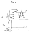
- FIG. 4 is a circuit diagram of a semiconductor memory device according to a third embodiment of the present invention.
- the SBD D S3 is incorporated in the manner shown in Fig. 4.
- This arrangement has the following two advantages. First, an optimum load characteristic can be obtained because a feedback path is created from a transistor Q 5 to a transistor Q 4 . Second, the value of the V F of the SBD D S3 can be shifted, in advance, to a desired value by suitably selecting the ratio between the values of resistors R 4 and R 5 .
- the semiconductor memory device can not only achieve high speed read/write operation, but can also finely cope with effects of variation of the forward voltage V F of Schottky barrier diodes in memory cells of the device.
Landscapes
- Engineering & Computer Science (AREA)
- Microelectronics & Electronic Packaging (AREA)
- Computer Hardware Design (AREA)
- Static Random-Access Memory (AREA)
- Semiconductor Memories (AREA)
Claims (4)
caractérisé en ce que
Applications Claiming Priority (2)
| Application Number | Priority Date | Filing Date | Title |
|---|---|---|---|
| JP213411/81 | 1981-12-29 | ||
| JP56213411A JPS6052520B2 (ja) | 1981-12-29 | 1981-12-29 | 半導体記憶装置 |
Publications (3)
| Publication Number | Publication Date |
|---|---|
| EP0084252A2 EP0084252A2 (fr) | 1983-07-27 |
| EP0084252A3 EP0084252A3 (en) | 1983-10-05 |
| EP0084252B1 true EP0084252B1 (fr) | 1986-07-16 |
Family
ID=16638779
Family Applications (1)
| Application Number | Title | Priority Date | Filing Date |
|---|---|---|---|
| EP82306888A Expired EP0084252B1 (fr) | 1981-12-29 | 1982-12-23 | Dispositif de mémoire à semi-conducteurs |
Country Status (5)
| Country | Link |
|---|---|
| US (1) | US4479200A (fr) |
| EP (1) | EP0084252B1 (fr) |
| JP (1) | JPS6052520B2 (fr) |
| DE (1) | DE3272052D1 (fr) |
| IE (1) | IE54335B1 (fr) |
Families Citing this family (15)
| Publication number | Priority date | Publication date | Assignee | Title |
|---|---|---|---|---|
| JPS6015892A (ja) * | 1983-07-08 | 1985-01-26 | Nec Corp | 基準電圧発生回路 |
| JPS6083291A (ja) * | 1983-10-13 | 1985-05-11 | Nec Corp | 半導体メモリ |
| JPS60253091A (ja) * | 1984-05-30 | 1985-12-13 | Fujitsu Ltd | 半導体記憶装置 |
| JPS61123168A (ja) * | 1984-11-20 | 1986-06-11 | Fujitsu Ltd | 半導体記憶装置 |
| US4845679A (en) * | 1987-03-30 | 1989-07-04 | Honeywell Inc. | Diode-FET logic circuitry |
| US4922455A (en) * | 1987-09-08 | 1990-05-01 | International Business Machines Corporation | Memory cell with active device for saturation capacitance discharge prior to writing |
| DE3882322T2 (de) * | 1987-09-30 | 1993-10-21 | Texas Instruments Inc | Statischer Speicher in Schottky-Technologie. |
| US5673218A (en) | 1996-03-05 | 1997-09-30 | Shepard; Daniel R. | Dual-addressed rectifier storage device |
| US5889694A (en) * | 1996-03-05 | 1999-03-30 | Shepard; Daniel R. | Dual-addressed rectifier storage device |
| US6956757B2 (en) | 2000-06-22 | 2005-10-18 | Contour Semiconductor, Inc. | Low cost high density rectifier matrix memory |
| US7813157B2 (en) * | 2007-10-29 | 2010-10-12 | Contour Semiconductor, Inc. | Non-linear conductor memory |
| US20090225621A1 (en) * | 2008-03-05 | 2009-09-10 | Shepard Daniel R | Split decoder storage array and methods of forming the same |
| US8325556B2 (en) | 2008-10-07 | 2012-12-04 | Contour Semiconductor, Inc. | Sequencing decoder circuit |
| CN103370790B (zh) | 2011-12-19 | 2016-01-20 | 松下电器产业株式会社 | 非易失性存储装置及其制造方法 |
| JP5406418B1 (ja) | 2012-03-29 | 2014-02-05 | パナソニック株式会社 | 不揮発性記憶装置 |
Family Cites Families (1)
| Publication number | Priority date | Publication date | Assignee | Title |
|---|---|---|---|---|
| US4057789A (en) * | 1974-06-19 | 1977-11-08 | International Business Machines Corporation | Reference voltage source for memory cells |
-
1981
- 1981-12-29 JP JP56213411A patent/JPS6052520B2/ja not_active Expired
-
1982
- 1982-12-23 DE DE8282306888T patent/DE3272052D1/de not_active Expired
- 1982-12-23 EP EP82306888A patent/EP0084252B1/fr not_active Expired
- 1982-12-27 US US06/453,110 patent/US4479200A/en not_active Expired - Fee Related
- 1982-12-30 IE IE3098/82A patent/IE54335B1/en unknown
Non-Patent Citations (1)
| Title |
|---|
| IEEE JOURNAL OF SOLID-STATE CIRCUITS, vol. SC-9, no. 5, October 1974, pages 283-284, New York, USA, H. MAYUMI et al.: "A 25-ns read access bipolar 1 kbit TTL RAM" * |
Also Published As
| Publication number | Publication date |
|---|---|
| EP0084252A2 (fr) | 1983-07-27 |
| JPS6052520B2 (ja) | 1985-11-19 |
| IE823098L (en) | 1983-06-29 |
| US4479200A (en) | 1984-10-23 |
| DE3272052D1 (en) | 1986-08-21 |
| EP0084252A3 (en) | 1983-10-05 |
| JPS58118087A (ja) | 1983-07-13 |
| IE54335B1 (en) | 1989-08-30 |
Similar Documents
| Publication | Publication Date | Title |
|---|---|---|
| US4999519A (en) | Semiconductor circuit with low power consumption having emitter-coupled logic or differential amplifier | |
| US4337523A (en) | Bipolar memory circuit | |
| US4479200A (en) | Semiconductor memory device | |
| GB1347438A (en) | Memory syxtem | |
| EP0023792B1 (fr) | Mémoire à semi-conducteurs comprenant des cellules intégrées à injection logique | |
| US4984207A (en) | Semiconductor memory device | |
| EP0090572B1 (fr) | Montage semi-conducteur d'amplificateur de détection | |
| US4057789A (en) | Reference voltage source for memory cells | |
| EP0218747A1 (fr) | Amplificateur de lecture destiné à amplifier les signaux d'une ligne polarisée | |
| KR0137711B1 (ko) | 바이폴라 및 전계 효과 트랜지스터에 의해 구현되고 안정된 감지 증폭기를 갖는 반도체 집적 회로 소자 | |
| JPH0316717B2 (fr) | ||
| US4424582A (en) | Semiconductor memory device | |
| US5138201A (en) | Sense amplifier operable under variable power supply voltage | |
| US4464735A (en) | Semiconductor memory | |
| EP0082695B1 (fr) | Dispositif de mémoire semi-conductrice | |
| EP0258627B1 (fr) | Commande de niveau logique pour logique à commutateurs de courant émetteurs suiveurs | |
| US4742488A (en) | Sense amplifier/write circuit for semiconductor memories | |
| US4272811A (en) | Write and read control circuit for semiconductor memories | |
| US5223744A (en) | Semiconductor integrated circuit with circuits for generating stable reference potential | |
| US4577296A (en) | Compensation current generator | |
| US4703458A (en) | Circuit for writing bipolar memory cells | |
| JPS61294686A (ja) | メモリ回路 | |
| US3876988A (en) | Associative memory | |
| JPS6020837B2 (ja) | 記憶装置 | |
| KR840001222B1 (ko) | 스태틱 메모리의 메모리 셀 장치 |
Legal Events
| Date | Code | Title | Description |
|---|---|---|---|
| PUAI | Public reference made under article 153(3) epc to a published international application that has entered the european phase |
Free format text: ORIGINAL CODE: 0009012 |
|
| AK | Designated contracting states |
Designated state(s): DE FR GB |
|
| PUAL | Search report despatched |
Free format text: ORIGINAL CODE: 0009013 |
|
| AK | Designated contracting states |
Designated state(s): DE FR GB |
|
| 17P | Request for examination filed |
Effective date: 19840216 |
|
| GRAA | (expected) grant |
Free format text: ORIGINAL CODE: 0009210 |
|
| AK | Designated contracting states |
Kind code of ref document: B1 Designated state(s): DE FR GB |
|
| ET | Fr: translation filed | ||
| REF | Corresponds to: |
Ref document number: 3272052 Country of ref document: DE Date of ref document: 19860821 |
|
| PLBE | No opposition filed within time limit |
Free format text: ORIGINAL CODE: 0009261 |
|
| STAA | Information on the status of an ep patent application or granted ep patent |
Free format text: STATUS: NO OPPOSITION FILED WITHIN TIME LIMIT |
|
| 26N | No opposition filed | ||
| PGFP | Annual fee paid to national office [announced via postgrant information from national office to epo] |
Ref country code: DE Payment date: 19890227 Year of fee payment: 7 |
|
| PG25 | Lapsed in a contracting state [announced via postgrant information from national office to epo] |
Ref country code: GB Effective date: 19891223 |
|
| GBPC | Gb: european patent ceased through non-payment of renewal fee | ||
| PG25 | Lapsed in a contracting state [announced via postgrant information from national office to epo] |
Ref country code: FR Effective date: 19900831 |
|
| PG25 | Lapsed in a contracting state [announced via postgrant information from national office to epo] |
Ref country code: DE Effective date: 19900901 |
|
| REG | Reference to a national code |
Ref country code: FR Ref legal event code: ST |