EP0084866A2 - Halbleitergehäuse - Google Patents
Halbleitergehäuse Download PDFInfo
- Publication number
- EP0084866A2 EP0084866A2 EP83100495A EP83100495A EP0084866A2 EP 0084866 A2 EP0084866 A2 EP 0084866A2 EP 83100495 A EP83100495 A EP 83100495A EP 83100495 A EP83100495 A EP 83100495A EP 0084866 A2 EP0084866 A2 EP 0084866A2
- Authority
- EP
- European Patent Office
- Prior art keywords
- base member
- casing
- metal
- alloy
- electrical component
- Prior art date
- Legal status (The legal status is an assumption and is not a legal conclusion. Google has not performed a legal analysis and makes no representation as to the accuracy of the status listed.)
- Withdrawn
Links
Images
Classifications
-
- H—ELECTRICITY
- H05—ELECTRIC TECHNIQUES NOT OTHERWISE PROVIDED FOR
- H05K—PRINTED CIRCUITS; CASINGS OR CONSTRUCTIONAL DETAILS OF ELECTRIC APPARATUS; MANUFACTURE OF ASSEMBLAGES OF ELECTRICAL COMPONENTS
- H05K1/00—Printed circuits
- H05K1/02—Details
- H05K1/0201—Thermal arrangements, e.g. for cooling, heating or preventing overheating
- H05K1/0203—Cooling of mounted components
- H05K1/021—Components thermally connected to metal substrates or heat-sinks by insert mounting
-
- H—ELECTRICITY
- H10—SEMICONDUCTOR DEVICES; ELECTRIC SOLID-STATE DEVICES NOT OTHERWISE PROVIDED FOR
- H10W—GENERIC PACKAGES, INTERCONNECTIONS, CONNECTORS OR OTHER CONSTRUCTIONAL DETAILS OF DEVICES COVERED BY CLASS H10
- H10W40/00—Arrangements for thermal protection or thermal control
- H10W40/20—Arrangements for cooling
- H10W40/22—Arrangements for cooling characterised by their shape, e.g. having conical or cylindrical projections
- H10W40/226—Arrangements for cooling characterised by their shape, e.g. having conical or cylindrical projections characterised by projecting parts, e.g. fins to increase surface area
-
- H—ELECTRICITY
- H10—SEMICONDUCTOR DEVICES; ELECTRIC SOLID-STATE DEVICES NOT OTHERWISE PROVIDED FOR
- H10W—GENERIC PACKAGES, INTERCONNECTIONS, CONNECTORS OR OTHER CONSTRUCTIONAL DETAILS OF DEVICES COVERED BY CLASS H10
- H10W70/00—Package substrates; Interposers; Redistribution layers [RDL]
- H10W70/40—Leadframes
- H10W70/421—Shapes or dispositions
- H10W70/424—Cross-sectional shapes
-
- H—ELECTRICITY
- H10—SEMICONDUCTOR DEVICES; ELECTRIC SOLID-STATE DEVICES NOT OTHERWISE PROVIDED FOR
- H10W—GENERIC PACKAGES, INTERCONNECTIONS, CONNECTORS OR OTHER CONSTRUCTIONAL DETAILS OF DEVICES COVERED BY CLASS H10
- H10W76/00—Containers; Fillings or auxiliary members therefor; Seals
- H10W76/10—Containers or parts thereof
- H10W76/12—Containers or parts thereof characterised by their shape
- H10W76/13—Containers comprising a conductive base serving as an interconnection
- H10W76/134—Containers comprising a conductive base serving as an interconnection having other interconnections parallel to the conductive base
-
- H—ELECTRICITY
- H10—SEMICONDUCTOR DEVICES; ELECTRIC SOLID-STATE DEVICES NOT OTHERWISE PROVIDED FOR
- H10W—GENERIC PACKAGES, INTERCONNECTIONS, CONNECTORS OR OTHER CONSTRUCTIONAL DETAILS OF DEVICES COVERED BY CLASS H10
- H10W76/00—Containers; Fillings or auxiliary members therefor; Seals
- H10W76/60—Seals
-
- H—ELECTRICITY
- H05—ELECTRIC TECHNIQUES NOT OTHERWISE PROVIDED FOR
- H05K—PRINTED CIRCUITS; CASINGS OR CONSTRUCTIONAL DETAILS OF ELECTRIC APPARATUS; MANUFACTURE OF ASSEMBLAGES OF ELECTRICAL COMPONENTS
- H05K1/00—Printed circuits
- H05K1/02—Details
- H05K1/03—Use of materials for the substrate
- H05K1/05—Insulated conductive substrates, e.g. insulated metal substrate
- H05K1/056—Insulated conductive substrates, e.g. insulated metal substrate the metal substrate being covered by an organic insulating layer
-
- H—ELECTRICITY
- H05—ELECTRIC TECHNIQUES NOT OTHERWISE PROVIDED FOR
- H05K—PRINTED CIRCUITS; CASINGS OR CONSTRUCTIONAL DETAILS OF ELECTRIC APPARATUS; MANUFACTURE OF ASSEMBLAGES OF ELECTRICAL COMPONENTS
- H05K1/00—Printed circuits
- H05K1/18—Printed circuits structurally associated with non-printed electric components
- H05K1/182—Printed circuits structurally associated with non-printed electric components associated with components mounted in printed circuit boards [PCB], e.g. insert-mounted components [IMC]
- H05K1/183—Printed circuits structurally associated with non-printed electric components associated with components mounted in printed circuit boards [PCB], e.g. insert-mounted components [IMC] associated with components mounted in and supported by recessed areas of the PCBs
-
- H—ELECTRICITY
- H05—ELECTRIC TECHNIQUES NOT OTHERWISE PROVIDED FOR
- H05K—PRINTED CIRCUITS; CASINGS OR CONSTRUCTIONAL DETAILS OF ELECTRIC APPARATUS; MANUFACTURE OF ASSEMBLAGES OF ELECTRICAL COMPONENTS
- H05K2201/00—Indexing scheme relating to printed circuits covered by H05K1/00
- H05K2201/10—Details of components or other objects attached to or integrated in a printed circuit board
- H05K2201/10613—Details of electrical connections of non-printed components, e.g. special leads
- H05K2201/10621—Components characterised by their electrical contacts
- H05K2201/10689—Leaded Integrated Circuit [IC] package, e.g. dual-in-line [DIL]
-
- H—ELECTRICITY
- H10—SEMICONDUCTOR DEVICES; ELECTRIC SOLID-STATE DEVICES NOT OTHERWISE PROVIDED FOR
- H10W—GENERIC PACKAGES, INTERCONNECTIONS, CONNECTORS OR OTHER CONSTRUCTIONAL DETAILS OF DEVICES COVERED BY CLASS H10
- H10W70/00—Package substrates; Interposers; Redistribution layers [RDL]
- H10W70/60—Insulating or insulated package substrates; Interposers; Redistribution layers
- H10W70/67—Insulating or insulated package substrates; Interposers; Redistribution layers characterised by their insulating layers or insulating parts
- H10W70/68—Shapes or dispositions thereof
- H10W70/682—Shapes or dispositions thereof comprising holes having chips therein
-
- H—ELECTRICITY
- H10—SEMICONDUCTOR DEVICES; ELECTRIC SOLID-STATE DEVICES NOT OTHERWISE PROVIDED FOR
- H10W—GENERIC PACKAGES, INTERCONNECTIONS, CONNECTORS OR OTHER CONSTRUCTIONAL DETAILS OF DEVICES COVERED BY CLASS H10
- H10W70/00—Package substrates; Interposers; Redistribution layers [RDL]
- H10W70/60—Insulating or insulated package substrates; Interposers; Redistribution layers
- H10W70/67—Insulating or insulated package substrates; Interposers; Redistribution layers characterised by their insulating layers or insulating parts
- H10W70/68—Shapes or dispositions thereof
- H10W70/685—Shapes or dispositions thereof comprising multiple insulating layers
-
- H—ELECTRICITY
- H10—SEMICONDUCTOR DEVICES; ELECTRIC SOLID-STATE DEVICES NOT OTHERWISE PROVIDED FOR
- H10W—GENERIC PACKAGES, INTERCONNECTIONS, CONNECTORS OR OTHER CONSTRUCTIONAL DETAILS OF DEVICES COVERED BY CLASS H10
- H10W72/00—Interconnections or connectors in packages
- H10W72/851—Dispositions of multiple connectors or interconnections
- H10W72/874—On different surfaces
- H10W72/884—Die-attach connectors and bond wires
-
- H—ELECTRICITY
- H10—SEMICONDUCTOR DEVICES; ELECTRIC SOLID-STATE DEVICES NOT OTHERWISE PROVIDED FOR
- H10W—GENERIC PACKAGES, INTERCONNECTIONS, CONNECTORS OR OTHER CONSTRUCTIONAL DETAILS OF DEVICES COVERED BY CLASS H10
- H10W90/00—Package configurations
- H10W90/701—Package configurations characterised by the relative positions of pads or connectors relative to package parts
- H10W90/731—Package configurations characterised by the relative positions of pads or connectors relative to package parts of die-attach connectors
- H10W90/736—Package configurations characterised by the relative positions of pads or connectors relative to package parts of die-attach connectors between a chip and a stacked lead frame, conducting package substrate or heat sink
-
- H—ELECTRICITY
- H10—SEMICONDUCTOR DEVICES; ELECTRIC SOLID-STATE DEVICES NOT OTHERWISE PROVIDED FOR
- H10W—GENERIC PACKAGES, INTERCONNECTIONS, CONNECTORS OR OTHER CONSTRUCTIONAL DETAILS OF DEVICES COVERED BY CLASS H10
- H10W90/00—Package configurations
- H10W90/701—Package configurations characterised by the relative positions of pads or connectors relative to package parts
- H10W90/751—Package configurations characterised by the relative positions of pads or connectors relative to package parts of bond wires
- H10W90/756—Package configurations characterised by the relative positions of pads or connectors relative to package parts of bond wires between a chip and a stacked lead frame, conducting package substrate or heat sink
Definitions
- the present invention is to a process and apparatus for encasing a semiconductor and more particularly for providing a highly reliable metal casing which is sealed and bonded using an adhesive.
- CERDIP hermetic ceramic dual in-line package
- Another technique known in the art is to enclose a semiconductor device in a metal package and to hermetically seal the package using cold pressure welding. This method. of hermetically sealing an electrical component in a metal housing is taught in U.S. Patent No. 2,999,194 to Boswell et al. and in U.S. Patent No. 3,988,825 to Fuchs et al.
- Adhesives have been used in the art to bond semiconductor packages as taught in U.S. Patent No. 3,740,.920,to Lane and in U.S. Patent No. 3,914,858 to Sonoda et al.
- a casing for an electrical component comprising a metal base member.
- a metal housing member is mounted on the base member to provide a hollow enclosed casing for receiving the electrical component.
- a metal lead frame is provided within the enclosed casing and is electrically connected to the electrical component.
- the lead frame has permanent leads projecting between the base member and the housing member external to the casing.
- the improvement may- include an element extending from the base member for strengthening the base member and providing additional heat transfer from the casing. Also, an adhesive seals and bonds the terminal leads to both the base member and to the housing member to form the enclosed casing.
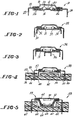
- a casing 10 for an electrical component 12 The casing comprises a metal base member 14.
- a metal housing -member 16 is mounted upon the base member 14 to provide a hollow enclosed casing for receiving the electrical component.
- a metal lead frame 18 within the enclosed casing is electrically connected by wires 20 to the electrical component.
- the lead frame 18 has terminal leads 22 and 24 projecting between the base member 14 and the housing member 16 external to the casing 10.
- the improvement comprises an adhesive 26 for sealing and bonding the terminal leads to both the base member and to the housing member to form the enclosed casing.
- the semiconductor element or chip 12 may be mounted on the bottom member using an epoxy adhesive as in any conventional plastic encapsulated package.
- the bottom surface of lead frame 18 is sealed and bonded to the bottom member 14 using an epoxy adhesive 26.
- An electrical connection between the chip 12 and the lead frame is made by wires 20 in a conventional manner.
- the housing member 16 is sealed and bonded to the top surface of the lead frame using epoxy 26.
- the terminal leads 22 and 24 project between the base member and the housing member external to the casing 10.
- the terminal leads preferably protrude from all sides of the casing, it is within the scope of the present invention for the terminal leads to extend from any number of sides.
- the housing member may be shaped to form a hollow enclosure as shown so as to not interfere with the chip or electrical wires 20.
- the exact shape of the casing 10 does not form a part of the present invention and may be any shape as desired.
- the metal used for the base member, the housing member, and the lead frame may be of any desired metal or alloy which bonds strongly with an adhesive.
- copper and copper base alloys having a refractory oxide layer provide very strong bonds with different adhesives and thereby prevent diffusion of contaminants between the epoxy and the metal substrate.
- Suitable copper base alloys for use in the present invention contain from 2 to 12% aluminum.
- CDA alloy 638 as disclosed in U.S. Patent No. 3,676,292 to Pryor et al., containing 2.5 to 3.1% aluminum, 1.5 to 2.1% silicon, and 0.25 to 0.55% cobalt is-most useful in the provision of a metal in accordance with this invention.
- Impurities may be present which do not prevent bonding in a desired environment. Further, it may be desirable to use CDA alloy 6381, as disclosed in U.S. Patent No. 3,341,369 to Caule et al. Alloy 6381 is similar to alloy 638 except for the omission of cobalt. This omission reduces cost and entails some reduction in annealed mechanical properties.
- the alloys useful with this invention and, especially alloys 638 or 6381, have a refractory oxide layer applied to the surface which is in contact with the adhesive.
- the oxide layer may include complex oxides formed with elements such as alumina, silica, tin, iron chromia, zinc, and manganese.
- the refractory oxide layer is substantially aluminum oxide (Al 2 O 3 ).
- This refractory oxide may be applied to the substrate. in any desired manner.
- a copper base alloy such as alloy 638 is preoxidized in gases having an extremely low oxygen content.
- the alloy 638 may be placed in a container with 4% hydrogen and 96% nitrogen and a trace of oxygen released from a trace of water mixed in the gas.
- This gas may be heated to a temperature of between about 330°C and about 820°C. Depending on the temperature and amount of time the alloy is left in the heated gas, a refractory oxide layer of a desired thickness forms on the surface of the alloy. It is also within the scope of the invention to apply the refractory oxide layer to the entire surface of each element in contact with the epoxy.
- alloy 638 with a preoxidized surface bonds well to adhesives, such as epoxies, and is, therefore, substantially impervious to the diffusion of contaminants between the epoxy and the metal substrate.
- the preoxidized surface is an excellent barrier to any contaminants passing directly through the metal.
- the casing of the present invention has reduced the potential for interdiffusion of contaminants since the majority of the package is metal and the interdiffusion can substantially only occur in the relatively thin layer of adhesive which seals the package.
- the present invention uses any adhesive 26 such as an epoxy which provides a strong bond with any metal or alloy and preferably with a metal or alloy having a refractory oxide surface layer such as preoxidized 638 or 6381.
- the substrate 14 provides the primary strength and stiffness to the package.
- the substrate is formed of alloy 638 or 6381 as mentioned above. Further, it is often necessary to provide heat dissipation through the substrate. In that case, the heat dissipation may be improved by cladding the 638 or 6381 with another alloy such as copper alloy 151 to provide greatly increased thermal conductivity. It is also within the scope of the present invention to clad any other metal or metal alloy with desired characteristics to a metal or alloy having a refractory oxide layer on at least one surface.
- Figure 2 is an illustration of a second embodiment 28. of the present invention which is similar to the embodiment of Figure 1.
- a peripheral skirt 30 has been added to the base member or substrate 31. Skirt 30 may extend from the corners 32 of substrate 31 at any desirable angle and preferably at approximately 90 degrees from the bottom surface 33 of the substrate 31.
- the skirt imparts additional strength and stiffness to substrate 31. The stiffening effect of the skirt may permit a substantial reduction in the thickness of the substrate and thereby provide a source of cost reduction.
- the skirt 30 also enhances the thermal dissipation of the substrate by providing additional heat transfer surface to increase convective heat transfer to. the air or environment.
- FIG 3 there is illustrated an embodiment 34 of the present invention, similar to the embodiment of Figure 2, but with additional cooling fins 36.
- the fins may be constructed of a strip or several strips of preferably high thermal conductivity alloy such as alloy 151 and joined to the bottom surface of substrate 31 by any conventional'manner such as soldering.
- the fins are illustrated as being a strip of material bent into a U-shaped configuration, it is within the scope of the present invention to provide any number of cooling fins formed from any number of strips of material with each being of any desirable shape.
- Figure 4 illustrates an embodiment 38 where a semiconductor casing 28 having a skirted substrate, substantially identical as with the embodiment of Figure 2, is joined to a printed circuit board 40 having a buried heat sink/ground plate 42 extending there through.
- the circuit board may be conventionally constructed from a metal or alloy layers 52 and 54 and bonded together by a material 56 such as a conventional organic epoxy.
- the ground plate 42 may be made of any material preferably having high thermal and electrical conductivity.
- the printed circuit board 40 includes through-holes 44 and 46 to receive the ends 48 and 50, respectively, of the lead frame 57.
- the through-holes may be plated so as to receive solder and join the outer layers 52 and 54.
- the skirt 30 may be placed in contact with the heat sink/ground plate 42 to enhance the heat dissipation from the package.
- the skirt is joined to the plate 42 by any desired means such as solder.
- Figure 5 illustrates another embodiment 58 of the present invention wherein a casing 59 includes a dropped center substrate 60.
- the substrate may be formed by deep drawing the material of the substrate by any conventional means such as stamping.
- the cover 62 may be substantially flat since the space required for the chip is provided by the shaped substrate.
- a hollow section 64 in the printed circuit board 65 permits a portion or area 66 of the substrate 60 to be joined, by any conventional means such as soldering, directly to a heat sink/ground plate 68 which is buried within the printed circuit board.
- the coefficient of thermal expansion of the substrate may be chosen to closely match that of the heat sink/ground plate 68. Thus, difficulties which might arise out of a mismatch of the coefficient of thermal expansion and in particular in the large joining area 66 are substantially eliminated.
- a layer 70 of moisture or contaminate absorbing material may be affixed to the internal surface 72 of lid 62 so as to scavenge water vapor and/or other contaminants which may diffuse into the package.
- This layer may consist of materials such as silica gel, activated carbon, etc., or mixtures of such materials.
- the material may be affixed in any conventional manner such as by an adhesive or placement in a container and affixing the container to the surface 72. Although this option is illustrated in Figure 5, it may also be applied to any embodiments provided herein and in any semiconductor package. Also, the material may be affixed to any desired inner surface.
Landscapes
- Engineering & Computer Science (AREA)
- Microelectronics & Electronic Packaging (AREA)
- Cooling Or The Like Of Semiconductors Or Solid State Devices (AREA)
Applications Claiming Priority (4)
| Application Number | Priority Date | Filing Date | Title |
|---|---|---|---|
| US06/341,392 US4461924A (en) | 1982-01-21 | 1982-01-21 | Semiconductor casing |
| US341392 | 1982-01-21 | ||
| US390095 | 1982-06-21 | ||
| US06/390,095 US4410927A (en) | 1982-01-21 | 1982-06-21 | Casing for an electrical component having improved strength and heat transfer characteristics |
Publications (1)
| Publication Number | Publication Date |
|---|---|
| EP0084866A2 true EP0084866A2 (de) | 1983-08-03 |
Family
ID=26992485
Family Applications (1)
| Application Number | Title | Priority Date | Filing Date |
|---|---|---|---|
| EP83100495A Withdrawn EP0084866A2 (de) | 1982-01-21 | 1983-01-20 | Halbleitergehäuse |
Country Status (2)
| Country | Link |
|---|---|
| US (1) | US4410927A (de) |
| EP (1) | EP0084866A2 (de) |
Cited By (7)
| Publication number | Priority date | Publication date | Assignee | Title |
|---|---|---|---|---|
| EP0129966A1 (de) * | 1983-04-22 | 1985-01-02 | Cray Research, Inc. | Schaltkreismodul mit Kühleinrichtung von hoher Wirksamkeit |
| US4535385A (en) * | 1983-04-22 | 1985-08-13 | Cray Research, Inc. | Circuit module with enhanced heat transfer and distribution |
| FR2560731A1 (fr) * | 1984-03-05 | 1985-09-06 | Telecommunications Sa | Carte imprimee multicouche thermoconductrice |
| EP0114917A3 (de) * | 1982-12-29 | 1986-03-19 | Olin Corporation | Halbleiterverkapselungen |
| GB2195048A (en) * | 1986-09-02 | 1988-03-23 | Int Rectifier Co Ltd | Semiconductor packages and connection techniques for use therewith |
| EP0338213A3 (de) * | 1988-02-22 | 1990-11-07 | Kabushiki Kaisha Toshiba | Halbleiterbauelement mit einem Metallgehäuse |
| EP0700083A3 (de) * | 1988-10-05 | 1996-04-10 | Olin Corp |
Families Citing this family (68)
| Publication number | Priority date | Publication date | Assignee | Title |
|---|---|---|---|---|
| GB2111312A (en) * | 1981-11-04 | 1983-06-29 | Philips Electronic Associated | Substrates for electrical circuits |
| US4866571A (en) * | 1982-06-21 | 1989-09-12 | Olin Corporation | Semiconductor package |
| US5014159A (en) * | 1982-04-19 | 1991-05-07 | Olin Corporation | Semiconductor package |
| US4513353A (en) * | 1982-12-27 | 1985-04-23 | Amp Incorporated | Connection of leadless integrated circuit package to a circuit board |
| SE435443B (sv) * | 1983-02-18 | 1984-09-24 | Ericsson Telefon Ab L M | Kylanordning for elektroniska komponenter vilka genom hallare er anslutna till kretskort |
| USRE32942E (en) * | 1983-10-06 | 1989-06-06 | Olin Corporation | Low thermal expansivity and high thermal conductivity substrate |
| JPS60116191A (ja) * | 1983-11-29 | 1985-06-22 | イビデン株式会社 | 電子部品搭載用基板の製造方法 |
| DE3402538A1 (de) * | 1984-01-26 | 1985-08-01 | Robert Bosch Gmbh, 7000 Stuttgart | Waermeableitende befestigung |
| US4736236A (en) * | 1984-03-08 | 1988-04-05 | Olin Corporation | Tape bonding material and structure for electronic circuit fabrication |
| US4628411A (en) * | 1984-03-12 | 1986-12-09 | International Business Machines Corporation | Apparatus for directly powering a multi-chip module from a power distribution bus |
| US4577056A (en) * | 1984-04-09 | 1986-03-18 | Olin Corporation | Hermetically sealed metal package |
| US4805009A (en) * | 1985-03-11 | 1989-02-14 | Olin Corporation | Hermetically sealed semiconductor package |
| US4801488A (en) * | 1984-09-19 | 1989-01-31 | Olin Corporation | Sealing glass composite |
| US4542259A (en) * | 1984-09-19 | 1985-09-17 | Olin Corporation | High density packages |
| US4775647A (en) * | 1984-09-19 | 1988-10-04 | Olin Corporation | Sealing glass composite |
| US4752521A (en) * | 1984-09-19 | 1988-06-21 | Olin Corporation | Sealing glass composite |
| US4840654A (en) * | 1985-03-04 | 1989-06-20 | Olin Corporation | Method for making multi-layer and pin grid arrays |
| US4771537A (en) * | 1985-12-20 | 1988-09-20 | Olin Corporation | Method of joining metallic components |
| US4821151A (en) * | 1985-12-20 | 1989-04-11 | Olin Corporation | Hermetically sealed package |
| IT1203535B (it) * | 1986-02-10 | 1989-02-15 | Marelli Autronica | Procedimento per la realizzazione del collegamento meccanico ed elettrico fra due corpi in particolare tra la membrana ed il sopporto di un sensore di pressione a film spesso e dispositivi realizzati con tale procedimento |
| US4793967A (en) * | 1986-03-12 | 1988-12-27 | Olin Corporation | Cermet substrate with spinel adhesion component |
| US4743299A (en) * | 1986-03-12 | 1988-05-10 | Olin Corporation | Cermet substrate with spinel adhesion component |
| US4812896A (en) * | 1986-11-13 | 1989-03-14 | Olin Corporation | Metal electronic package sealed with thermoplastic having a grafted metal deactivator and antioxidant |
| US4721831A (en) * | 1987-01-28 | 1988-01-26 | Unisys Corporation | Module for packaging and electrically interconnecting integrated circuit chips on a porous substrate, and method of fabricating same |
| US4769345A (en) * | 1987-03-12 | 1988-09-06 | Olin Corporation | Process for producing a hermetically sealed package for an electrical component containing a low amount of oxygen and water vapor |
| US4751401A (en) * | 1987-03-23 | 1988-06-14 | Core Industries Inc. | Low voltage switch |
| US4993148A (en) * | 1987-05-19 | 1991-02-19 | Mitsubishi Denki Kabushiki Kaisha | Method of manufacturing a circuit board |
| US4839716A (en) * | 1987-06-01 | 1989-06-13 | Olin Corporation | Semiconductor packaging |
| US4827376A (en) * | 1987-10-05 | 1989-05-02 | Olin Corporation | Heat dissipating interconnect tape for use in tape automated bonding |
| US4849857A (en) * | 1987-10-05 | 1989-07-18 | Olin Corporation | Heat dissipating interconnect tape for use in tape automated bonding |
| US5016138A (en) * | 1987-10-27 | 1991-05-14 | Woodman John K | Three dimensional integrated circuit package |
| US4783428A (en) * | 1987-11-23 | 1988-11-08 | Motorola Inc. | Method of producing a thermogenetic semiconductor device |
| US4796156A (en) * | 1987-12-04 | 1989-01-03 | General Electric Company | Self packaging chip mount |
| US4908736A (en) * | 1987-12-04 | 1990-03-13 | General Electric Company | Self packaging chip mount |
| US4888449A (en) * | 1988-01-04 | 1989-12-19 | Olin Corporation | Semiconductor package |
| US4897508A (en) * | 1988-02-10 | 1990-01-30 | Olin Corporation | Metal electronic package |
| US5013871A (en) * | 1988-02-10 | 1991-05-07 | Olin Corporation | Kit for the assembly of a metal electronic package |
| US5023398A (en) * | 1988-10-05 | 1991-06-11 | Olin Corporation | Aluminum alloy semiconductor packages |
| US5155299A (en) * | 1988-10-05 | 1992-10-13 | Olin Corporation | Aluminum alloy semiconductor packages |
| US4975761A (en) * | 1989-09-05 | 1990-12-04 | Advanced Micro Devices, Inc. | High performance plastic encapsulated package for integrated circuit die |
| US5237205A (en) * | 1989-10-02 | 1993-08-17 | Advanced Micro Devices, Inc. | Ground plane for plastic encapsulated integrated circuit die packages |
| US5559369A (en) * | 1989-10-02 | 1996-09-24 | Advanced Micro Devices, Inc. | Ground plane for plastic encapsulated integrated circuit die packages |
| US4953109A (en) * | 1989-10-16 | 1990-08-28 | Design-Rite, Inc. | Automated trash compactor system |
| US5043534A (en) * | 1990-07-02 | 1991-08-27 | Olin Corporation | Metal electronic package having improved resistance to electromagnetic interference |
| JP2913891B2 (ja) * | 1990-12-04 | 1999-06-28 | 三菱電機株式会社 | 多層配線基板 |
| EP0511162A1 (de) * | 1991-04-24 | 1992-10-28 | Ciba-Geigy Ag | Wärmeleitende Klebfilme, Laminate mit wärmeleitenden Klebschichten und deren Verwendung |
| US6111308A (en) * | 1991-06-05 | 2000-08-29 | Advanced Micro Devices, Inc. | Ground plane for plastic encapsulated integrated circuit die packages |
| US5284706A (en) * | 1991-12-23 | 1994-02-08 | Olin Corporation | Sealing glass composite |
| US5328870A (en) * | 1992-01-17 | 1994-07-12 | Amkor Electronics, Inc. | Method for forming plastic molded package with heat sink for integrated circuit devices |
| JPH06120374A (ja) * | 1992-03-31 | 1994-04-28 | Amkor Electron Inc | 半導体パッケージ構造、半導体パッケージ方法及び半導体パッケージ用放熱板 |
| DE9300865U1 (de) * | 1993-01-22 | 1994-05-26 | Siemens AG, 80333 München | Einstückiges Kunststoffteil, insbesondere Spritzgießteil |
| US5701034A (en) * | 1994-05-03 | 1997-12-23 | Amkor Electronics, Inc. | Packaged semiconductor die including heat sink with locking feature |
| JPH08204059A (ja) * | 1995-01-20 | 1996-08-09 | Kyocera Corp | 半導体素子収納用パッケージ |
| US6175084B1 (en) | 1995-04-12 | 2001-01-16 | Denki Kagaku Kogyo Kabushiki Kaisha | Metal-base multilayer circuit substrate having a heat conductive adhesive layer |
| US5710695A (en) * | 1995-11-07 | 1998-01-20 | Vlsi Technology, Inc. | Leadframe ball grid array package |
| DE19808986A1 (de) * | 1998-03-03 | 1999-09-09 | Siemens Ag | Halbleiterbauelement mit mehreren Halbleiterchips |
| US6084297A (en) * | 1998-09-03 | 2000-07-04 | Micron Technology, Inc. | Cavity ball grid array apparatus |
| US6535396B1 (en) * | 2000-04-28 | 2003-03-18 | Delphi Technologies, Inc. | Combination circuit board and segmented conductive bus substrate |
| US6639757B2 (en) | 2001-01-10 | 2003-10-28 | Hutchinson Technology Inc. | Heat dissipation structures for integrated lead disk drive head suspensions |
| US6545227B2 (en) | 2001-07-11 | 2003-04-08 | Mce/Kdi Corporation | Pocket mounted chip having microstrip line |
| JP2003092158A (ja) * | 2001-09-19 | 2003-03-28 | Mitsubishi Electric Corp | 表面実装用コネクタおよびこれを用いた半導体モジュール |
| US6841263B2 (en) * | 2002-05-03 | 2005-01-11 | The John Hopkins University | Method of adhering a solid polymer to a substrate and resulting article |
| DE112004000007T5 (de) * | 2003-01-28 | 2005-08-11 | Cmk Corp. | Mehrschicht-Leiterplatte mit Metallkern |
| US20090145802A1 (en) * | 2007-12-11 | 2009-06-11 | Apple Inc. | Storage system for components incorporating a liquid-metal thermal interface |
| JP4961398B2 (ja) * | 2008-06-30 | 2012-06-27 | 株式会社日立製作所 | 半導体装置 |
| CN101975376B (zh) * | 2010-10-08 | 2012-07-11 | 深圳市华星光电技术有限公司 | 背光模块的发光源散热构造 |
| US20160099200A1 (en) * | 2014-10-01 | 2016-04-07 | Stmicroelectronics S.R.L. | Aluminum alloy lead frame for a semiconductor device and corresponding manufacturing process |
| USD1049066S1 (en) * | 2022-02-28 | 2024-10-29 | Syskey Technology Co., Ltd. | Base for a multi-chamber semiconductor |
Family Cites Families (15)
| Publication number | Priority date | Publication date | Assignee | Title |
|---|---|---|---|---|
| GB818464A (en) * | 1956-03-12 | 1959-08-19 | Gen Electric Co Ltd | Improvements in or relating to semiconductor devices |
| US3113252A (en) * | 1958-02-28 | 1963-12-03 | Gen Motors Corp | Means for encapsulating transistors |
| US3341369A (en) * | 1965-03-03 | 1967-09-12 | Olin Mathieson | Copper base alloys and process for preparing same |
| US3374537A (en) * | 1965-03-22 | 1968-03-26 | Philco Ford Corp | Method of connecting leads to a semiconductive device |
| US3480836A (en) * | 1966-08-11 | 1969-11-25 | Ibm | Component mounted in a printed circuit |
| US3469017A (en) * | 1967-12-12 | 1969-09-23 | Rca Corp | Encapsulated semiconductor device having internal shielding |
| US3676292A (en) * | 1970-10-07 | 1972-07-11 | Olin Corp | Composites of glass-ceramic-to-metal,seals and method of making same |
| US3740920A (en) * | 1971-05-26 | 1973-06-26 | Us Air Force | Method for packaging hybrid circuits |
| DE2158188A1 (de) * | 1971-11-24 | 1973-06-07 | Jenaer Glaswerk Schott & Gen | Kaltpresschweissbare und kaltpressloetbare druckglasdurchfuehrungen |
| US3739232A (en) * | 1972-04-10 | 1973-06-12 | Northrop Corp | Interconnected electrical circuit board assembly and method of fabrication |
| US3872583A (en) * | 1972-07-10 | 1975-03-25 | Amdahl Corp | LSI chip package and method |
| US4066839A (en) * | 1972-11-16 | 1978-01-03 | Sgs-Ates Componenti Elettronici S.P.A. | Molded body incorporating heat dissipator |
| US3914858A (en) * | 1974-08-23 | 1975-10-28 | Nitto Electric Ind Co | Method of making sealed cavity molded semiconductor devices |
| US4262165A (en) * | 1976-03-26 | 1981-04-14 | Hitachi, Ltd. | Packaging structure for semiconductor IC chip |
| US4320438A (en) * | 1980-05-15 | 1982-03-16 | Cts Corporation | Multi-layer ceramic package |
-
1982
- 1982-06-21 US US06/390,095 patent/US4410927A/en not_active Expired - Lifetime
-
1983
- 1983-01-20 EP EP83100495A patent/EP0084866A2/de not_active Withdrawn
Cited By (7)
| Publication number | Priority date | Publication date | Assignee | Title |
|---|---|---|---|---|
| EP0114917A3 (de) * | 1982-12-29 | 1986-03-19 | Olin Corporation | Halbleiterverkapselungen |
| EP0129966A1 (de) * | 1983-04-22 | 1985-01-02 | Cray Research, Inc. | Schaltkreismodul mit Kühleinrichtung von hoher Wirksamkeit |
| US4535385A (en) * | 1983-04-22 | 1985-08-13 | Cray Research, Inc. | Circuit module with enhanced heat transfer and distribution |
| FR2560731A1 (fr) * | 1984-03-05 | 1985-09-06 | Telecommunications Sa | Carte imprimee multicouche thermoconductrice |
| GB2195048A (en) * | 1986-09-02 | 1988-03-23 | Int Rectifier Co Ltd | Semiconductor packages and connection techniques for use therewith |
| EP0338213A3 (de) * | 1988-02-22 | 1990-11-07 | Kabushiki Kaisha Toshiba | Halbleiterbauelement mit einem Metallgehäuse |
| EP0700083A3 (de) * | 1988-10-05 | 1996-04-10 | Olin Corp |
Also Published As
| Publication number | Publication date |
|---|---|
| US4410927A (en) | 1983-10-18 |
Similar Documents
| Publication | Publication Date | Title |
|---|---|---|
| US4410927A (en) | Casing for an electrical component having improved strength and heat transfer characteristics | |
| US4461924A (en) | Semiconductor casing | |
| US4524238A (en) | Semiconductor packages | |
| US4480262A (en) | Semiconductor casing | |
| US4594770A (en) | Method of making semiconductor casing | |
| US4897508A (en) | Metal electronic package | |
| EP0594395B1 (de) | Leistungshalbleitermodul | |
| US5519936A (en) | Method of making an electronic package with a thermally conductive support member having a thin circuitized substrate and semiconductor device bonded thereto | |
| US6873043B2 (en) | Electronic assembly having electrically-isolated heat-conductive structure | |
| US4656499A (en) | Hermetically sealed semiconductor casing | |
| US4542259A (en) | High density packages | |
| US5311060A (en) | Heat sink for semiconductor device assembly | |
| US4784974A (en) | Method of making a hermetically sealed semiconductor casing | |
| US5577656A (en) | Method of packaging a semiconductor device | |
| JPH11330283A (ja) | 半導体モジュール及び大型半導体モジュール | |
| GB2274352A (en) | Electronic device packaging assembly | |
| US5804873A (en) | Heatsink for surface mount device for circuit board mounting | |
| US5200640A (en) | Hermetic package having covers and a base providing for direct electrical connection | |
| CN87104825A (zh) | 散热性能改善了的大规模集成电路封装 | |
| JPH0773117B2 (ja) | 半導体パッケ−ジ | |
| US5093713A (en) | Semiconductor device package | |
| CA1201211A (en) | Hermetically sealed semiconductor casing | |
| US12532750B2 (en) | Clip for a discrete power semiconductor package | |
| CN100583421C (zh) | 用于垂直安装的半导体封装结构及方法 | |
| JPS622587A (ja) | ハイパワ−用混成集積回路 |
Legal Events
| Date | Code | Title | Description |
|---|---|---|---|
| PUAI | Public reference made under article 153(3) epc to a published international application that has entered the european phase |
Free format text: ORIGINAL CODE: 0009012 |
|
| AK | Designated contracting states |
Designated state(s): DE FR GB IT |
|
| 17P | Request for examination filed |
Effective date: 19840203 |
|
| STAA | Information on the status of an ep patent application or granted ep patent |
Free format text: STATUS: THE APPLICATION IS DEEMED TO BE WITHDRAWN |
|
| 18D | Application deemed to be withdrawn |
Effective date: 19850801 |
|
| RIN1 | Information on inventor provided before grant (corrected) |
Inventor name: BUTT, SHELDON H. |