EP0086447A2 - Dispositif semi-conducteur capteur d'images couleur - Google Patents
Dispositif semi-conducteur capteur d'images couleur Download PDFInfo
- Publication number
- EP0086447A2 EP0086447A2 EP83101203A EP83101203A EP0086447A2 EP 0086447 A2 EP0086447 A2 EP 0086447A2 EP 83101203 A EP83101203 A EP 83101203A EP 83101203 A EP83101203 A EP 83101203A EP 0086447 A2 EP0086447 A2 EP 0086447A2
- Authority
- EP
- European Patent Office
- Prior art keywords
- filter
- filter element
- horizontal line
- covered
- picture element
- Prior art date
- Legal status (The legal status is an assumption and is not a legal conclusion. Google has not performed a legal analysis and makes no representation as to the accuracy of the status listed.)
- Granted
Links
Images






Classifications
-
- H—ELECTRICITY
- H04—ELECTRIC COMMUNICATION TECHNIQUE
- H04N—PICTORIAL COMMUNICATION, e.g. TELEVISION
- H04N25/00—Circuitry of solid-state image sensors [SSIS]; Control thereof
- H04N25/10—Circuitry of solid-state image sensors [SSIS]; Control thereof for transforming different wavelengths into image signals
- H04N25/11—Arrangement of colour filter arrays [CFA]; Filter mosaics
- H04N25/13—Arrangement of colour filter arrays [CFA]; Filter mosaics characterised by the spectral characteristics of the filter elements
- H04N25/135—Arrangement of colour filter arrays [CFA]; Filter mosaics characterised by the spectral characteristics of the filter elements based on four or more different wavelength filter elements
- H04N25/136—Arrangement of colour filter arrays [CFA]; Filter mosaics characterised by the spectral characteristics of the filter elements based on four or more different wavelength filter elements using complementary colours
-
- H—ELECTRICITY
- H10—SEMICONDUCTOR DEVICES; ELECTRIC SOLID-STATE DEVICES NOT OTHERWISE PROVIDED FOR
- H10F—INORGANIC SEMICONDUCTOR DEVICES SENSITIVE TO INFRARED RADIATION, LIGHT, ELECTROMAGNETIC RADIATION OF SHORTER WAVELENGTH OR CORPUSCULAR RADIATION
- H10F39/00—Integrated devices, or assemblies of multiple devices, comprising at least one element covered by group H10F30/00, e.g. radiation detectors comprising photodiode arrays
- H10F39/10—Integrated devices
- H10F39/12—Image sensors
- H10F39/15—Charge-coupled device [CCD] image sensors
- H10F39/153—Two-dimensional or three-dimensional array CCD image sensors
- H10F39/1538—Time-delay and integration
-
- H—ELECTRICITY
- H10—SEMICONDUCTOR DEVICES; ELECTRIC SOLID-STATE DEVICES NOT OTHERWISE PROVIDED FOR
- H10F—INORGANIC SEMICONDUCTOR DEVICES SENSITIVE TO INFRARED RADIATION, LIGHT, ELECTROMAGNETIC RADIATION OF SHORTER WAVELENGTH OR CORPUSCULAR RADIATION
- H10F39/00—Integrated devices, or assemblies of multiple devices, comprising at least one element covered by group H10F30/00, e.g. radiation detectors comprising photodiode arrays
- H10F39/10—Integrated devices
- H10F39/12—Image sensors
- H10F39/15—Charge-coupled device [CCD] image sensors
- H10F39/156—CCD or CID colour image sensors
Definitions
- the present invention relates to an improvement in a solid state color imaging apparatus.
- the present invention especially concerns a solid state color imaging appratus comprising a solid state imaging sensor having a plurality of photoelectric elements disposed in two-dimensional rows and are specially patterned color filter intended to attain high-horizontal resolution, high S/N ratio and simple signal processing.
- a solid state image sensor is, as is well known, an apparatus for converting objective image to an electric signal.
- a single chip solid state color camera is an apparatus comprising a solid state imaging sensor and color filter with elements of different colors in front of the solid state imaging sensor, thereby to to obtain an objective image on the surface of the solid state image sensor, which produces spatially modulated chrominance signal and luminance signal to enable to synthesize .a composite color signal.
- the solid state image sensor is a kind of a large scale integrated circuit (LSI), and therefore in order to obtain a high production yield, degree of the integration of the device should be preferably low. Therefore, the number of the photoelectric elements, disposed in a two dimensional pattern on a substrate, namely the number of picture element, should be as small as possible under a condition for attaining a required resolution of image. Accordingly, the way of producing chrominance signal should be that which does not lower theoretical value of the resolution attainable for the number of picture elements. Many proposals have been made for the modes of the pattern combination between the picture elements and the color filter thereof, and main stream thereof are those using mosaic color filter.
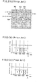
- FIG. 1 shows a fundamental type apparatus which uses a color filter having filter pattern of vertical color stripes comprising repetion of three primary colors in a horizontal direction.
- the apparatus has a solid state image sensor having a number of photoelectric elements, i.e., picture elements 101 disposed forming vertical rows and horizontal lines, and a color filter having vertical color stripes of green filter stripes 102, red filter stripes 103 and blue filter stripes 104 disposed repeatedly in turn.
- the chrominance signals for colors of the color filter are modulated by respective color filter stripes.
- the carrier frequency of the chrominance signal is one third (1/3) of the sampling frequency f s by the picture elements.
- the band-width of signal of the objective image sampled by picture elements is a half (1/2) of the sampling frequency of the picture elements.
- the frequency range usable for the luminance signal band has to be limited under 1 ⁇ 3f S (one third of the sampling frequency), resulting in a disadvantage of lowering of horizontal resolution.
- FIG. 2 shows another.conventinal example wherein green filter elements 202 are disposed in staggered way with respect to the photoelectric picture elements 201, and for other picture elements in the n-th line (for instance, odd number lines) R ( red) filters 203 are disposed and for other picture elements in (n+l)-th lines (for instance, even order lines) B(blue) filters 204 are disposed.
- n-th line for instance, odd number lines
- red filters 203 red
- n+l-th lines for instance, even order lines
- B(blue) filters 204 are disposed.
- FIG. 3 there are other conventional example as shown in FIG. 3.
- n-th line e.g., odd number line
- red filter 303 2/3 of the area is covered by red filter 303 and the rest 1/3 area is covered by green filter 305 and in next picture element in the same horizontal direction
- green filter 305 2/3 area is covered by blue filter 304 and remaining 1/3 area is by green filter, and the same pair repeats in the same order in that line.
- blue filter 304 i.e. (n+l)-th line
- luminance signal S Yn for the n-th line and luminance .signal S Y(n+1) for (n+l) -th line are given by the following equations(l) and (2):
- the luminance signal can be easily obtained only by taking out through a low-path filter, without complicated sampling process as shown in the example of FIG. 2.
- this conventional example has a difficulty of making the filter so as to be registrated with the picture elements in a manner to divide the picture element into 2/3 areas and 1/3 areas.
- the chrominance signal spatially modulated for n-th lines and (n+l)-th lines are given by the following equations (3) and (4), respectively: where K 1 is a constant.
- the modulated chrominance signals have components of primary color signals in the amounts of 2/3. Accordingly, the S/N ratio is low. As shown in equations (1) and (2) , the luminance signals become in the amunt of 2/3 of the primary color signals R, G and B, accordingly S/N ratios of the luminance signal also is not sufficiantly high.
- the present invention purposes to provide a solid state color imaging apparatus having an improved luminance level differences between sequence of scanning lines, having improved S/N ratio of chrominance signal without lowering resolution of picture which is given by number of picture elements of the solid state image sensor.
- the luminance signal can be separated by a simple circuit comprising a low-pass filter without generation of luminance level differences between sequence of scanning lines, thereby both the luminance signal and chrominance signal are easily processed.
- the present invention is suitable for a small type color video camera apparatus aiming high resolution and high chrominance S/N ratio.
- a solid state color imaging apparatus in accordance with the present invention comprises:
- said first color light is blue and said second color light is green and said third light is red
- said first horizontal line is, for instance, odd number horizontal lines and said second horizontal line is even number horizontal lines.
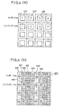
- FIG. 4(a) shows a front view of picture elements disposition of a solid state imagge sensor wherein picture elements are disposed regularly in horizontal lines and vertical rows, and hereinafter one every other lines are referred as n-th horizontal lines and the other lines alternately disposed between the above lines are referred as (n+l)-th lines.
- n-th line for instance, odd number lines
- a first picture element 401 is divided into with vertical line around at center and left half is covered with MG filter 402 and right half is covered with CY filter 403, and next for second picture element is also divided into two parts and left part is covered with G filter 403' and its right part is covered with YE filter 404.
- the G filter is made by superposing extended part of the CY filter 403 and the extended part of the YE filter 404. And the above-mentioned filter color arrangement is repeated in the same order in the n-th horizontal lines.
- MG filter and G filter are disposed in vertical stripes and CY filter and Y E filter are disposed alternatively or staggerdly in vertical rows.
- a mosaic pattern filter 405 is constituted.
- the G filters may be formed not by superposition of CY and YE filters but with proper G filters.
- chrominance signals are produced in respective picture elements corresponding to filter colors covering them as follows, provided that photoelectric conversion characteristic of the photodiode in the solid state image sensor is flat for wavelength range of 400 nm-700 nm:
- sum of signal outputs (photodiode outputs) corresponding to respective incident light through respective color filters are as follows under the same premise as the n-th line on the spectrum characteristic of the photodiodes:
- signal 'output S nH for n-th line and S (n+1) H for (n+l)-th line are given as follows: wherein the second terms represent time sequential change of chrominance signal part and first terms represent mean value, namely luminance signal part.
- the low frequency components Sy of the signal is as follows:
- the luminance signal S Y is obtainable without luminance level difference between sequence of scanning lines by simply taking it through a low-pass filter.
- the modulated color difference signal is given as alternating appearance of the belowmentioned components: And the carrier frequency of the modulated chrominance signal is f C , which is 1/2 of the sampling frequency f S . Accordingly, band width of the luminance signal S Y can be extended to theoretical limit of Nykist's condition.
- the hatched parts show modulated color differential part S C , as shown in FIG. 6.
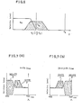
- FIG. 7(a) and FIG. 7(b) schematically show spectrum distributions of respective primary color components of modulated color difference signals S C , respectively for n-th line and (n+l)-th line.
- the spectral distributions based on first picture element is shown by solid lines and spectral distributions based on the second picture elements are shown by dotted lines.
- signal level for the first picture element is given by as shown by solid line in FIG. 7 (a)
- signal level for the second picture element is given by as shown by dotted line in FIG. 7 (a).
- a component signal designated by a hatched region b and the other ccmponent signal designated by the other hatched region are modulated with spatial frequency of the picture element dispositions. Therefore, the modulated signal is given by the term of
- signal level for the first picture element is given by as shown by solid line in FIG. 7(b)
- signal level for the second picture element is given by as shown by dotted line in FIG. 7(b).
- a component signal designated by a hatched region r and the other component signal designated by the other hatched region are modulated with spatial frequency of the picture element dispositions. Therefore, the modulated signal is given by the term of
- the above-mentioned explanation has been made under a condition that spectral characteristic of the photoelectric device is a flat for the range of 400 nm-700 nm, but in actual solid state imaging sensor the photoelectric sensitivity extends to infrared range, and in order to compensate this an infrared cut off filter is used. Accordingly, in actual imaging apparatus provided with the infrared cut filter in front of the photodiode picture elements, the output from the picture elements has spectral distribution of a product of spectral characteristic of the solid state imaging sensor itself and the spectral characteristic of the infrared cut filter.
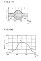
- FIG. 7(e) shows one example of the spectral characteristic which is a product of solid state imaging sensor and infrared cut filter.
- the curve shows that resultant sensitivity decreases on both of red side (600-700 nm) and in blue side (400-500 nm). Accordingly, by obtaining a product of this spectral distribution and the spectral distributions of FIG. 7(a) and FIG. 7(b), the actual spectral distributions for n-th line and (n+l)-th line are obtained as shown in FIG. 7(c) and FIG. 7(d), respectively, wherein hatched parts show modulated color differential component parts.
- FIG. 7(e) shows one example of the spectral characteristic which is a product of solid state imaging sensor and infrared cut filter.
- the curve shows that resultant sensitivity decreases on both of red side (600-700 nm) and in blue side (400-500 nm). Accordingly, by obtaining a product of this spectral distribution and the spectral
- amplitudes of chrominance signals to be spatially modulated for an n-th line and (n+I) -th line are r - and b - , respectively, which are different from the color difference signal r - y, b - y in NTSC TV signal.
- the color difference signals r - and b - which are obtained directly from the solid state image sensor by using the modulating phases p - and b - shown in FIG. 8, the two color difference signals are equivalently handled to a modulated chrominance signal made with phases of r - y and b - y, respectively.
- FIG. 9(a) schematically shows overall distribution of component signals of luminance signal in an actual example, wherein dotted curve shows overall spectral characteristic and hatched area shows component outputs.
- the sum of the total signal Y is as shown in FIG. 9(a)
- the overall spectral distribution is low both in short wavelength part and long wavelength part
- the spectral distribution shown in FIG. 9(a) is fairly approximate to the actual contents of luminance signal Y' of NTSC standard which is given by:
- FIG. 9 (b) shows an actual overall spectral characteristic curve of the apparatus, obtained by multiplying spectral characteristic of FIG. 7(e) for infrared-cut filter, and composite spectral characteristic of FIG. 9(a).
- FIG. 10 shows a circuit diagram of one example for processing the above-mentioned signals.
- block 1001 designates the solid state imaging sensor shown in FIG. 4(a) and FIG. 4(b), and its output signal is given to a low-pass filter 1002 having cut off frequency f c for separately outputting the luminance signal component Y.
- the output signal of the solid state imaging sensor 1001 is also given to a band-path filter 1003 having a center frequency f for separately issuing spatially modulated color difference signals and give it to a detection circuit 1004. Then, the detection circuit 1004 issues time sequential color difference signals r - and b - .
- this time sequential signals are given to a timing adjusting circuit 1308 which comprises one-horizontal-line time delay circuit 1005 and switching circuit 1006 for selectively passing by alternately switching every one horizontal period.
- the output signals r - and b - given through the switching circuit 1006 are given to encoder 1007 where the luminance signal Y is also given to and the encoder 1007 composes.standard NTSC output by processing the three input signals and issues to the output terminal 1008. If white balance is changed greatly, color difference signals do not become zero, even when a white object is photographed due to some inbalance or dispersion of spectral characteristics of illumination source or filters. In such case, the inbalance can be compensated by adding or subtracting a part of the luminance signal Y to or from the color difference signals given to the encoder 1007.
- the spatial modulated component attributable to the mosaic filter is made in such a manner that
- the part of the second picture element constituted by superposing two kinds of filters can be replaced by a single filter which has equivalent characteristic to the superposed filters.
- the apparatus in accordance with the present invention can provide a color imaging apparatus capable of producing luminance signals having primary color signal component ratio considerably approximate to the standard NTSC system. And also, the spatial modulation of the color difference signal is large and accordingly, S/N ratio of the chrominance signal becomes large.
- luminance signal obtained does not have luminance level differences between sequence of scanning lines even when a correlation circuit is dispenced with.
- band-width of luminance signal can be made to 1 of the sampling frequency, accordingly a high horizontal 2 resolution up to theoretical limit.
- FIG. 11(a) shows a second example in accordance with the present invention having different color filter patterns.
- every picture elements are divided into two segments by a vertical dividing line and covered with different color filters. That isin the example of FIG. 11(a) in n-th line, for instance, odd number lines, a first picture element 1101 is divided into two parts with vertical line around at center and left half is covered with MG filter 1102, and right half is covered with R filter 1104. Next, for second picture element, for instance, second picture element is also divided into two parts and left part is covered with CY filter 1103 and right part is covered with G filter 1106.
- the G filter can be made by superposing extended part of the CY filter 1103 and the narrow Y E filter 1107. And the above-mentioned filter color arrangement is repeated in the same order in the n-th horizontal lines.
- the MG filters and G filters are disposed in vertical stripes and R filter and B filter as well as CY filter and YE filter, are arranged making vertically repeating dispositions.
- a mosaic pattern filter 1100 is constituted.
- the B filter may be formed by superposing MG filter and CY filter
- the G filter may be formed by superposing YE filter and CY filter.
- the G filters may be formed not by superposing the CY filter and YE filters, but with proper G filters.
- chrominance signals are produced in respective picture elements corresponding to filter colors covering them as follows, provided that photoelectric conversion characteristic of the photodiode in the solid state image sensor is flat for wavelength range of 400 nm ⁇ 700 nm:
- sum of signal outputs (photodiode outputs) corresponding to respective incident light through respective color filters are as follows under the same premise as the n-th line on the spectrum characteristic of the photodiodes;
- mean chrominance output S YnH for n-th line and S Y(n+1)H for (n+l)-th line are given as follows: where K 15 and K 11 are constants.
- FIG. 11(b) and FIG. ll(c) The situation of this is shown in FIG. 11(b) and FIG. ll(c) for n-th lines and (n+l)-th lines, respectively.
- the luminance signal S Y without luminance level differences between sequence of scanning lines is obtainable by simply taking it through a low-pass filter.
- the carrier f C of chrominance signal to be spatially modulated is at 1 ⁇ 2f S as shown in FIG. 11(d), and accordingly, band width of luminance signal S Y can be extended to the limit of Nykist's condition, and high resolution corresponding to theoretical limit of the picture element density is attainable.
- FIG. 11(e) and FIG. 11(f) Spatially modulated color difference signals for n-th line and (n+1)-th line are shown in FIG. 11(e) and FIG. 11(f), respectively.
- the spatially modulated color difference signals for n-th line is r - g and for (n+1)-th line is b - g, and therefore is larger by 50% than the conventional example of FIG. 3 (b) and FIG. 3(c), as is obvious when equations (3) and (4) are compared, and therefore good S/N ratio is attainable.
- FIG. 12 shows further example. In this example, the similar effect as that of the preceding examples of FIG. 4(b) or FIG. 11(a) is obtainable.
- FIG. 12 shows further example. In this example, the similar effect as that of the preceding examples of FIG. 4(b) or FIG. 11(a) is obtainable.
- FIG. 11(a) Spatially modulated color difference signals for n-th line and (n+1)-th line
- the left half part of the picture element is covered with YE filter and the right part thereof is covered with R filter
- the left part is covered with B filter and its right part is covered with CY filter.
- the R filter is constituted by superposing the YE filter and MG filter
- the B filter is constituted by superposing the CY filter and the MG filter.
- (n+l)-th line the whole part of the first picture element is covered with MG filter, and the whole part of the second picture element is covered with G filter. And this pair of MG. and G filter is repeated in the (n+l)-th line.
- the G filter is constituted by superposing the YE filter and cy filter. And the n-th line and (n+l)-th line are alternately disposed in vertical direction so that mosaic filter pattern as the FIG. 12(a) is constituted.
- the sum of the signal becomes substantially flat and equal for n-th line and (n+l)-th line as shown by FIG. 12(b) and FIG. 12(c), respectively.
- the luminance signal can be separated without making luminanee level differences between sequence of scanning lines, since there is no difference between sum of signal between the alternate horizontal lines. Furthermore, since the periods of horizontal repetition of the color filters is for two picture elements width, the carrier frequency f C of chrominance signal generated by spatial modulation by the color filters become a half (1 ⁇ 2) of the sampling frequency f s by the picture elements. Accordingly, the band width of the luminance signal can be extended to the frequency of 1 ⁇ 2f s , and accordingly, the horizontal resolution can be raised to theoretical value decided by the horizontal density of the picture elements.
- the above-mentioned color difference signals are represented in FIG. 12 (e) for n-th lines, and in FIG. 12(f) for (n+l)-th lines, respectively.
- the present example can produce a larger output signal in comparison with the conventional example shown in FIG. 3(a) and accordingly, an apparatus of good S/N ratio is obtainable.
- FIG. 13 shows one example of circuit diagram for processing signals for the solid state imaging sensor of FIG. ll(a) and FIG. 12(a).
- output signal from the solid state imaging sensor 1001' is given to a first low-pass filter 1002, a second low-pass filter 1312 and a band-pass filter 1003.
- the modulated color difference signal is given to a detector 1004, which issues detected.output.signals to time adjusting circuit 1308 which comprises one horizontal period delay circuit 1005 and selection switch 1006.
- the output signal of the selection switch 1006 are given to white balancer 1309 to which output signal from the second low-pass filter -1312 is also given as reference signal.
- output signals of the white balancer 1309 and luminance signal Y from the low-pass filter 1002 are given to an encoder 1007 which synthesizes known standard NTSC signal and output it to the output terminal 1008.
- the solid state color imaging apparatus in accordance with the present invention can produce luminance signal which has information of high resolution as theoretically given corresponding to the number of picture elements. And further, only by employing low-pass filter, the luminance signal is easily separated luminance level differences between sequence of scanning lines.
- the present apparatus is suitable for small type solid state color imaging apparatus.
Landscapes
- Physics & Mathematics (AREA)
- Spectroscopy & Molecular Physics (AREA)
- Engineering & Computer Science (AREA)
- Multimedia (AREA)
- Signal Processing (AREA)
- Color Television Image Signal Generators (AREA)
Applications Claiming Priority (4)
| Application Number | Priority Date | Filing Date | Title |
|---|---|---|---|
| JP22325/82 | 1982-02-15 | ||
| JP57022325A JPS58139586A (ja) | 1982-02-15 | 1982-02-15 | カラ−固体撮像装置 |
| JP57072103A JPS58188983A (ja) | 1982-04-28 | 1982-04-28 | 固体カラ−撮像装置 |
| JP72103/82 | 1982-04-28 |
Publications (3)
| Publication Number | Publication Date |
|---|---|
| EP0086447A2 true EP0086447A2 (fr) | 1983-08-24 |
| EP0086447A3 EP0086447A3 (en) | 1984-10-10 |
| EP0086447B1 EP0086447B1 (fr) | 1989-01-18 |
Family
ID=26359522
Family Applications (1)
| Application Number | Title | Priority Date | Filing Date |
|---|---|---|---|
| EP83101203A Expired EP0086447B1 (fr) | 1982-02-15 | 1983-02-08 | Dispositif semi-conducteur capteur d'images couleur |
Country Status (4)
| Country | Link |
|---|---|
| US (1) | US4630106A (fr) |
| EP (1) | EP0086447B1 (fr) |
| CA (1) | CA1203893A (fr) |
| DE (1) | DE3379021D1 (fr) |
Cited By (9)
| Publication number | Priority date | Publication date | Assignee | Title |
|---|---|---|---|---|
| DE3434765A1 (de) * | 1983-09-22 | 1985-04-11 | Rca Corp., New York, N.Y. | Farbteiler, beispielsweise fuer eine fernsehkamera |
| EP0289044A3 (fr) * | 1987-04-30 | 1990-01-24 | Kabushiki Kaisha Toshiba | Détecteur d'images couleur et son procédé de fabrication |
| EP0281554A4 (fr) * | 1985-03-01 | 1990-06-05 | Manchester R & D Partnership | Affichage a cristaux liquides a couleurs complementaires. |
| GB2240901A (en) * | 1989-12-31 | 1991-08-14 | Samsung Electronics Co Ltd | Primary colour forming circuit for complementary colour filter charge coupled device |
| US5142389A (en) * | 1985-03-01 | 1992-08-25 | Manchester R & D Limited Partnership | Liquid crystal color display and method |
| US5168380A (en) * | 1985-03-01 | 1992-12-01 | Manchester R & D Partnership An Ohio Limited Partnership | Multiple containment mediums of operationally nematic liquid crystal responsive to a prescribed input |
| US5208686A (en) * | 1985-03-01 | 1993-05-04 | Manchester R&D Partnership | Liquid crystal color display and method |
| US5345322A (en) * | 1985-03-01 | 1994-09-06 | Manchester R&D Limited Partnership | Complementary color liquid crystal display |
| EP0766480A3 (fr) * | 1995-09-28 | 2000-03-01 | Kabushiki Kaisha Toshiba | Appareil de prise de vues en couleur à l'état solide |
Families Citing this family (6)
| Publication number | Priority date | Publication date | Assignee | Title |
|---|---|---|---|---|
| DE3312962A1 (de) * | 1982-04-12 | 1983-10-13 | Canon K.K., Tokyo | Bildaufnahmevorrichtung |
| US4979136A (en) * | 1988-03-01 | 1990-12-18 | Transitions Research Corporation | Processing system and method for enhancing image data |
| US4896207A (en) * | 1988-06-17 | 1990-01-23 | Eastman Kodak Company | Color imaging apparatus employing a horizontal stripe color filter to reduce rise-time artifacts |
| US5115302A (en) * | 1990-04-26 | 1992-05-19 | Sharp Kabushiki Kaisha | Solid state color imaging device |
| KR0186183B1 (ko) * | 1995-12-19 | 1999-03-20 | 문정환 | 컬러 고체촬상소자 |
| US6330029B1 (en) * | 1998-03-17 | 2001-12-11 | Eastman Kodak Company | Particular pattern of pixels for a color filter array which is used to derive luminance and chrominance values |
Family Cites Families (7)
| Publication number | Priority date | Publication date | Assignee | Title |
|---|---|---|---|---|
| US3982274A (en) * | 1974-09-03 | 1976-09-21 | Bell Telephone Laboratories, Incorporated | Color coding filter for charge-coupled-device camera |
| JPS6056030B2 (ja) * | 1975-10-24 | 1985-12-07 | 松下電器産業株式会社 | カラー固体撮像装置 |
| JPS5592089A (en) * | 1978-12-29 | 1980-07-12 | Matsushita Electric Ind Co Ltd | Color solid image pickup device |
| US4288812A (en) * | 1979-11-19 | 1981-09-08 | Rca Corporation | Color filter |
| JPS5684089A (en) * | 1979-12-12 | 1981-07-09 | Matsushita Electric Ind Co Ltd | Solid-state color image pickup device |
| JPS574679A (en) * | 1980-06-11 | 1982-01-11 | Matsushita Electric Ind Co Ltd | Color solid-state pickup device |
| JPS5875394A (ja) * | 1981-10-29 | 1983-05-07 | Sharp Corp | 単板カラ−撮像装置 |
-
1983
- 1983-02-04 US US06/463,666 patent/US4630106A/en not_active Expired - Lifetime
- 1983-02-08 EP EP83101203A patent/EP0086447B1/fr not_active Expired
- 1983-02-08 DE DE8383101203T patent/DE3379021D1/de not_active Expired
- 1983-02-14 CA CA000421558A patent/CA1203893A/fr not_active Expired
Cited By (10)
| Publication number | Priority date | Publication date | Assignee | Title |
|---|---|---|---|---|
| DE3434765A1 (de) * | 1983-09-22 | 1985-04-11 | Rca Corp., New York, N.Y. | Farbteiler, beispielsweise fuer eine fernsehkamera |
| EP0281554A4 (fr) * | 1985-03-01 | 1990-06-05 | Manchester R & D Partnership | Affichage a cristaux liquides a couleurs complementaires. |
| US5142389A (en) * | 1985-03-01 | 1992-08-25 | Manchester R & D Limited Partnership | Liquid crystal color display and method |
| US5168380A (en) * | 1985-03-01 | 1992-12-01 | Manchester R & D Partnership An Ohio Limited Partnership | Multiple containment mediums of operationally nematic liquid crystal responsive to a prescribed input |
| US5208686A (en) * | 1985-03-01 | 1993-05-04 | Manchester R&D Partnership | Liquid crystal color display and method |
| US5345322A (en) * | 1985-03-01 | 1994-09-06 | Manchester R&D Limited Partnership | Complementary color liquid crystal display |
| EP0289044A3 (fr) * | 1987-04-30 | 1990-01-24 | Kabushiki Kaisha Toshiba | Détecteur d'images couleur et son procédé de fabrication |
| US4951130A (en) * | 1987-04-30 | 1990-08-21 | Kabushiki Kaisha Toshiba | Color filter structure of color image sensor |
| GB2240901A (en) * | 1989-12-31 | 1991-08-14 | Samsung Electronics Co Ltd | Primary colour forming circuit for complementary colour filter charge coupled device |
| EP0766480A3 (fr) * | 1995-09-28 | 2000-03-01 | Kabushiki Kaisha Toshiba | Appareil de prise de vues en couleur à l'état solide |
Also Published As
| Publication number | Publication date |
|---|---|
| DE3379021D1 (en) | 1989-02-23 |
| EP0086447B1 (fr) | 1989-01-18 |
| US4630106A (en) | 1986-12-16 |
| CA1203893A (fr) | 1986-04-29 |
| EP0086447A3 (en) | 1984-10-10 |
Similar Documents
| Publication | Publication Date | Title |
|---|---|---|
| EP0272634B1 (fr) | Dispositif de génération de signal vidéo | |
| EP0086447B1 (fr) | Dispositif semi-conducteur capteur d'images couleur | |
| EP0119862B1 (fr) | Appareil monolithique de prise d'images en couleur | |
| US5063439A (en) | Solid state pickup system having improved color reproducibility | |
| US4670777A (en) | Color filter having cyan, yellow, green and magenta filter elements providing increased dynamic range for use with field integration mode solid state imaging device | |
| CA1151287A (fr) | Filtre optique teinte | |
| EP2680589A1 (fr) | Dispositif d'imagerie couleur | |
| US4688085A (en) | Enhanced sensitivity color video camera with reduced red component in second luminance signal | |
| EP0141167B1 (fr) | Dispositif d'analyse d'image du type à l'état solide comportant un filtre coloré | |
| JPH06335006A (ja) | 固体撮像装置 | |
| US4282547A (en) | Color image pick-up apparatus | |
| US4450475A (en) | Solid state color imaging apparatus | |
| JPH0345593B2 (fr) | ||
| US4517588A (en) | Color solid state image pick-up device | |
| US4339771A (en) | Solid-state color imaging apparatus having an excellent resolution | |
| US5168350A (en) | Solid-state color imaging apparatus | |
| EP0098559B1 (fr) | Dispositif de prise de vues en couleur à corps solide | |
| EP0034361B1 (fr) | Dispositif de prise de vues en couleur à l'état solide | |
| EP0053318A1 (fr) | Dispositif de prise de vues en couleur à l'état solide | |
| JPH06339145A (ja) | カラー撮像装置 | |
| JPH0712218B2 (ja) | カラ−固体撮像装置 | |
| JPH0640670B2 (ja) | 固体撮像装置 | |
| US4389666A (en) | Color television camera system | |
| JPH0156593B2 (fr) | ||
| JPH0139273B2 (fr) |
Legal Events
| Date | Code | Title | Description |
|---|---|---|---|
| PUAI | Public reference made under article 153(3) epc to a published international application that has entered the european phase |
Free format text: ORIGINAL CODE: 0009012 |
|
| AK | Designated contracting states |
Designated state(s): DE FR GB |
|
| PUAL | Search report despatched |
Free format text: ORIGINAL CODE: 0009013 |
|
| RHK1 | Main classification (correction) |
Ipc: H04N 9/04 |
|
| AK | Designated contracting states |
Designated state(s): DE FR GB |
|
| 17P | Request for examination filed |
Effective date: 19850401 |
|
| 17Q | First examination report despatched |
Effective date: 19870311 |
|
| GRAA | (expected) grant |
Free format text: ORIGINAL CODE: 0009210 |
|
| AK | Designated contracting states |
Kind code of ref document: B1 Designated state(s): DE FR GB |
|
| REF | Corresponds to: |
Ref document number: 3379021 Country of ref document: DE Date of ref document: 19890223 |
|
| ET | Fr: translation filed | ||
| PLBE | No opposition filed within time limit |
Free format text: ORIGINAL CODE: 0009261 |
|
| STAA | Information on the status of an ep patent application or granted ep patent |
Free format text: STATUS: NO OPPOSITION FILED WITHIN TIME LIMIT |
|
| 26N | No opposition filed | ||
| REG | Reference to a national code |
Ref country code: GB Ref legal event code: 746 Effective date: 19950224 |
|
| REG | Reference to a national code |
Ref country code: FR Ref legal event code: D6 |
|
| PGFP | Annual fee paid to national office [announced via postgrant information from national office to epo] |
Ref country code: FR Payment date: 19990209 Year of fee payment: 17 |
|
| PGFP | Annual fee paid to national office [announced via postgrant information from national office to epo] |
Ref country code: GB Payment date: 19990211 Year of fee payment: 17 |
|
| PGFP | Annual fee paid to national office [announced via postgrant information from national office to epo] |
Ref country code: DE Payment date: 19990212 Year of fee payment: 17 |
|
| PG25 | Lapsed in a contracting state [announced via postgrant information from national office to epo] |
Ref country code: GB Free format text: LAPSE BECAUSE OF NON-PAYMENT OF DUE FEES Effective date: 20000208 |
|
| PG25 | Lapsed in a contracting state [announced via postgrant information from national office to epo] |
Ref country code: DE Free format text: LAPSE BECAUSE OF NON-PAYMENT OF DUE FEES Effective date: 20000229 |
|
| GBPC | Gb: european patent ceased through non-payment of renewal fee |
Effective date: 20000208 |
|
| PG25 | Lapsed in a contracting state [announced via postgrant information from national office to epo] |
Ref country code: FR Free format text: LAPSE BECAUSE OF NON-PAYMENT OF DUE FEES Effective date: 20001031 |
|
| REG | Reference to a national code |
Ref country code: FR Ref legal event code: ST |