EP0087112B1 - Multi purpose chip - Google Patents
Multi purpose chip Download PDFInfo
- Publication number
- EP0087112B1 EP0087112B1 EP83101446A EP83101446A EP0087112B1 EP 0087112 B1 EP0087112 B1 EP 0087112B1 EP 83101446 A EP83101446 A EP 83101446A EP 83101446 A EP83101446 A EP 83101446A EP 0087112 B1 EP0087112 B1 EP 0087112B1
- Authority
- EP
- European Patent Office
- Prior art keywords
- substrate
- lead
- circuit devices
- connections
- circuit
- Prior art date
- Legal status (The legal status is an assumption and is not a legal conclusion. Google has not performed a legal analysis and makes no representation as to the accuracy of the status listed.)
- Expired
Links
Images

Classifications
-
- H—ELECTRICITY
- H01—ELECTRIC ELEMENTS
- H01C—RESISTORS
- H01C17/00—Apparatus or processes specially adapted for manufacturing resistors
- H01C17/006—Apparatus or processes specially adapted for manufacturing resistors adapted for manufacturing resistor chips
-
- H—ELECTRICITY
- H01—ELECTRIC ELEMENTS
- H01C—RESISTORS
- H01C13/00—Resistors not provided for elsewhere
- H01C13/02—Structural combinations of resistors
-
- H—ELECTRICITY
- H01—ELECTRIC ELEMENTS
- H01C—RESISTORS
- H01C17/00—Apparatus or processes specially adapted for manufacturing resistors
- H01C17/22—Apparatus or processes specially adapted for manufacturing resistors adapted for trimming
- H01C17/23—Apparatus or processes specially adapted for manufacturing resistors adapted for trimming by opening or closing resistor geometric tracks of predetermined resistive values, e.g. snapistors
-
- H—ELECTRICITY
- H10—SEMICONDUCTOR DEVICES; ELECTRIC SOLID-STATE DEVICES NOT OTHERWISE PROVIDED FOR
- H10W—GENERIC PACKAGES, INTERCONNECTIONS, CONNECTORS OR OTHER CONSTRUCTIONAL DETAILS OF DEVICES COVERED BY CLASS H10
- H10W20/00—Interconnections in chips, wafers or substrates
- H10W20/40—Interconnections external to wafers or substrates, e.g. back-end-of-line [BEOL] metallisations or vias connecting to gate electrodes
- H10W20/49—Adaptable interconnections, e.g. fuses or antifuses
Definitions
- the present invention relates to a circuit structure according to the preamble of claim 1.
- a circuit structure is for example known from GB-A-1 552 144. It is disclosed there a chip with a substrate and a plurality of circuit devices on the substrate related to each other in a predetermined sequence, and having severable conductive paths, with input and output connections, whereby encapsulating means are provided, which further comprises a lead having connections to each of the plurality of circuit devices and a parallel circuit for such connected devices that can control the by-pass or use of all, some or none of the connected devices.
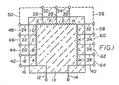
- a lead frame with an input 12 and an output 14 is connected about the substrate to have connections 16, 18, 20, 22, 24, 26, 28, 30, 32, 34, 36, 38 and 40 connected to each of the distinct areas.
- a conductive path is provided between these connections by means of structural links 42, 44, 46, 48, 50, 52, 54, 56, 58, 60, 62 and 64.
- These links sometimes referred to as shorting links, are typically constructed as tabs that are scribed so as to permit simple breakaway when a portion of the circuit provided by the lead frame is to be opened. This will be more particularly described with reference to Fig. 3 hereinafter.
- thin film resistors in terms of sheet resistance, i.e., the resistance measured between terminals 12 and 14 which are molecularly bonded to the entire sides of opposite ends of the thin film resistor.
- the value of a thin film resistor made of a material with a given sheet resistance will be size related and is usually expressed in ohms per square.
- resistors are formed and trimmed, e.g., trimmed by a laser, to create a path of connected squares whose width and length are controlled to provide a predetermined resistive impedance.
- This invention draws upon such prior art practices in resolving a preferred embodiment for a resistor according to this invention 4096 OHMIV values in a binary code of twelve (12) bits.
- an encapsulated chip is shown to comprise an epoxy housing 66 with binary code for the twelve bit design, i.e., R/2 through R/4096 preceding each tab 42 through 64.
- FIG. 3 This construction is opened for viewing by Fig. 3 showing the substrate 10 encircled by a flat lead frame 68 with input/output connections 12 and 14 and resistance connections, as shown.
- the tabs are scored as at 70 so that they can be simply broken away from the lead frame 68.
- the opening of a path through a particular resistance area is not dependent on the impedance value in protection of the chip as with prior art devices that use fusible link technology on the substrate.
- the practicality to the user is enhanced in allowing the device to be factory trimmed as regards resistance value and their binary sequence with field selection the resistance combinations for a desired impedance value for the chip in use in the field.
Landscapes
- Engineering & Computer Science (AREA)
- Microelectronics & Electronic Packaging (AREA)
- Manufacturing & Machinery (AREA)
- Apparatuses And Processes For Manufacturing Resistors (AREA)
- Use Of Switch Circuits For Exchanges And Methods Of Control Of Multiplex Exchanges (AREA)
- Mechanical Treatment Of Semiconductor (AREA)
- Photoreceptors In Electrophotography (AREA)
- Lead Frames For Integrated Circuits (AREA)
- Details Of Resistors (AREA)
- Channel Selection Circuits, Automatic Tuning Circuits (AREA)
- Coils Or Transformers For Communication (AREA)
- Fixed Capacitors And Capacitor Manufacturing Machines (AREA)
- Preparation Of Compounds By Using Micro-Organisms (AREA)
- Nitrogen Condensed Heterocyclic Rings (AREA)
- Pharmaceuticals Containing Other Organic And Inorganic Compounds (AREA)
- Lubricants (AREA)
- Diaphragms For Electromechanical Transducers (AREA)
- Semiconductor Integrated Circuits (AREA)
Priority Applications (1)
| Application Number | Priority Date | Filing Date | Title |
|---|---|---|---|
| AT83101446T ATE19839T1 (de) | 1982-02-19 | 1983-02-16 | Mehrzweck-chip. |
Applications Claiming Priority (2)
| Application Number | Priority Date | Filing Date | Title |
|---|---|---|---|
| US350209 | 1982-02-19 | ||
| US06/350,209 US4484213A (en) | 1982-02-19 | 1982-02-19 | Binary weighted resistor and package |
Publications (2)
| Publication Number | Publication Date |
|---|---|
| EP0087112A1 EP0087112A1 (en) | 1983-08-31 |
| EP0087112B1 true EP0087112B1 (en) | 1986-05-14 |
Family
ID=23375690
Family Applications (1)
| Application Number | Title | Priority Date | Filing Date |
|---|---|---|---|
| EP83101446A Expired EP0087112B1 (en) | 1982-02-19 | 1983-02-16 | Multi purpose chip |
Country Status (9)
| Country | Link |
|---|---|
| US (1) | US4484213A (da) |
| EP (1) | EP0087112B1 (da) |
| JP (1) | JPS59500590A (da) |
| AT (1) | ATE19839T1 (da) |
| DE (1) | DE3363471D1 (da) |
| DK (1) | DK459883A (da) |
| FI (1) | FI833789A0 (da) |
| NO (1) | NO833795L (da) |
| WO (1) | WO1983003030A1 (da) |
Families Citing this family (8)
| Publication number | Priority date | Publication date | Assignee | Title |
|---|---|---|---|---|
| US5146172A (en) * | 1990-08-15 | 1992-09-08 | Sundstrand Corp. | Engine identification system |
| US5635894A (en) * | 1993-12-23 | 1997-06-03 | The Boeing Company | Hi reliability fault tolerant terminating resistor |
| US5534788A (en) * | 1994-12-09 | 1996-07-09 | National Semiconductor Corporation | Integrated resistor for sensing electrical parameters |
| US6150714A (en) * | 1997-09-19 | 2000-11-21 | Texas Instruments Incorporated | Current sense element incorporated into integrated circuit package lead frame |
| TWI229387B (en) * | 2004-03-11 | 2005-03-11 | Au Optronics Corp | Laser annealing apparatus and laser annealing process |
| KR101582335B1 (ko) * | 2008-10-29 | 2016-01-04 | 삼성전자주식회사 | 휴대용 단말기에서 전압 강하 보상 장치 및 방법 |
| JP6938118B2 (ja) * | 2016-06-27 | 2021-09-22 | Koa株式会社 | 表面実装形薄膜抵抗ネットワーク |
| DE102016013454A1 (de) * | 2016-11-02 | 2018-05-03 | Wabco Gmbh | Hubkolbenmaschine, insbesondere ein- zwei- oder mehrstufiger Kolbenkompressor, Druckluftversorgungsanlage, Druckluftversorgungssystem und Fahrzeug, insbesondere PKW mit einer Druckluftversorgungsanlage, Verfahren zur Montage und zum Betrieb einer Hubkolbe |
Family Cites Families (9)
| Publication number | Priority date | Publication date | Assignee | Title |
|---|---|---|---|---|
| US3202952A (en) * | 1961-05-23 | 1965-08-24 | Illinois Tool Works | Wafer mounted component capable of electrical adjustment |
| GB1112992A (en) * | 1964-08-18 | 1968-05-08 | Texas Instruments Inc | Three-dimensional integrated circuits and methods of making same |
| US3441804A (en) * | 1966-05-02 | 1969-04-29 | Hughes Aircraft Co | Thin-film resistors |
| US3638162A (en) * | 1970-05-04 | 1972-01-25 | Gulf & Western Ind Prod Co | Programable electric circuit card |
| JPS51138179A (en) * | 1975-05-23 | 1976-11-29 | Seiko Instr & Electronics Ltd | Semi-conductor device |
| US4172249A (en) * | 1977-07-11 | 1979-10-23 | Vishay Intertechnology, Inc. | Resistive electrical components |
| FR2398374A1 (fr) * | 1977-07-19 | 1979-02-16 | Lignes Telegraph Telephon | Ajustement de resistances pour circuits hybrides |
| US4134096A (en) * | 1977-11-10 | 1979-01-09 | Allen-Bradley Company | Trimmable resistor |
| DE3012436A1 (de) * | 1980-03-31 | 1981-10-15 | Licentia Patent-Verwaltungs-Gmbh, 6000 Frankfurt | Bewertungswiderstandsanordnung fuer heizkoerperfuehler |
-
1982
- 1982-02-19 US US06/350,209 patent/US4484213A/en not_active Expired - Fee Related
- 1982-02-22 FI FI833789A patent/FI833789A0/fi not_active Application Discontinuation
- 1982-02-22 WO PCT/US1983/000230 patent/WO1983003030A1/en not_active Ceased
-
1983
- 1983-02-16 AT AT83101446T patent/ATE19839T1/de not_active IP Right Cessation
- 1983-02-16 DE DE8383101446T patent/DE3363471D1/de not_active Expired
- 1983-02-16 EP EP83101446A patent/EP0087112B1/en not_active Expired
- 1983-02-22 JP JP58501129A patent/JPS59500590A/ja active Pending
- 1983-10-05 DK DK459883A patent/DK459883A/da not_active Application Discontinuation
- 1983-10-18 NO NO833795A patent/NO833795L/no unknown
Non-Patent Citations (1)
| Title |
|---|
| MICROELECTRONICS JOURNAL, vol. 8, no. 4, June 1978, pages 18-24, Mackintosch Publications Ltd., Luton, G.B., D.E. WHEATLEY: "Active trimming of microchip resistors to 0.002 per cent" * |
Also Published As
| Publication number | Publication date |
|---|---|
| DK459883D0 (da) | 1983-10-05 |
| DE3363471D1 (en) | 1986-06-19 |
| DK459883A (da) | 1983-10-05 |
| FI833789A7 (fi) | 1983-10-17 |
| US4484213A (en) | 1984-11-20 |
| WO1983003030A1 (en) | 1983-09-01 |
| FI833789L (fi) | 1983-10-17 |
| NO833795L (no) | 1983-10-18 |
| FI833789A0 (fi) | 1983-10-17 |
| JPS59500590A (ja) | 1984-04-05 |
| ATE19839T1 (de) | 1986-05-15 |
| EP0087112A1 (en) | 1983-08-31 |
Similar Documents
| Publication | Publication Date | Title |
|---|---|---|
| US4641114A (en) | Thick film delay line comprising a plurality of stacked delay assemblies formed by a printing process | |
| EP0360540A2 (en) | Programmable logic device | |
| EP0087112B1 (en) | Multi purpose chip | |
| US5572779A (en) | Method of making an electronic thick film component multiple terminal | |
| JPS5652441A (en) | Programmable bit shift circuit | |
| US3983528A (en) | Resistor network with adjustable resistance value | |
| US5006735A (en) | Method and apparatus for compensating a solid state attenuator | |
| US20030154456A1 (en) | Resistor circuit | |
| US3026417A (en) | Photoconductive devices | |
| US3656115A (en) | Fusible link matrix for programmable networks | |
| EP0696818A2 (de) | Halbleiterbauelement mit isolierendem Gehäuse | |
| EP0230761A3 (en) | Resistive circuit arrangement | |
| US4565000A (en) | Matching of resistor sensitivities to process-induced variations in resistor widths | |
| EP0251212A3 (en) | Series resistive network | |
| EP0154399A3 (en) | Film resistor trimming | |
| KR920009079A (ko) | 집적회로 및 게이트 어레이 | |
| JPH07254830A (ja) | 電子ボリューム回路 | |
| JPS59161109A (ja) | 可変利得増幅器 | |
| US4507620A (en) | Ultra-rapid hybrid linear amplifier | |
| CA1129059A (en) | Circuit board for input rack assembly | |
| US4586019A (en) | Matching of resistor sensitivities to process-induced variations in resistor widths | |
| JPS62224901A (ja) | 厚膜抵抗装置 | |
| US4646056A (en) | Matching of resistor sensitivities to process-induced variations in resistor widths | |
| JP2823743B2 (ja) | 半導体集積装置 | |
| JP2767647B2 (ja) | 可変抵抗器 |
Legal Events
| Date | Code | Title | Description |
|---|---|---|---|
| PUAI | Public reference made under article 153(3) epc to a published international application that has entered the european phase |
Free format text: ORIGINAL CODE: 0009012 |
|
| AK | Designated contracting states |
Designated state(s): AT BE CH DE FR GB IT LI LU NL SE |
|
| 17P | Request for examination filed |
Effective date: 19831102 |
|
| ITF | It: translation for a ep patent filed | ||
| GRAA | (expected) grant |
Free format text: ORIGINAL CODE: 0009210 |
|
| AK | Designated contracting states |
Kind code of ref document: B1 Designated state(s): AT BE CH DE FR GB IT LI LU NL SE |
|
| REF | Corresponds to: |
Ref document number: 19839 Country of ref document: AT Date of ref document: 19860515 Kind code of ref document: T |
|
| REF | Corresponds to: |
Ref document number: 3363471 Country of ref document: DE Date of ref document: 19860619 |
|
| ET | Fr: translation filed | ||
| PLBE | No opposition filed within time limit |
Free format text: ORIGINAL CODE: 0009261 |
|
| STAA | Information on the status of an ep patent application or granted ep patent |
Free format text: STATUS: NO OPPOSITION FILED WITHIN TIME LIMIT |
|
| 26N | No opposition filed | ||
| PGFP | Annual fee paid to national office [announced via postgrant information from national office to epo] |
Ref country code: GB Payment date: 19910215 Year of fee payment: 9 |
|
| PGFP | Annual fee paid to national office [announced via postgrant information from national office to epo] |
Ref country code: SE Payment date: 19910218 Year of fee payment: 9 Ref country code: CH Payment date: 19910218 Year of fee payment: 9 |
|
| PGFP | Annual fee paid to national office [announced via postgrant information from national office to epo] |
Ref country code: LU Payment date: 19910220 Year of fee payment: 9 |
|
| PGFP | Annual fee paid to national office [announced via postgrant information from national office to epo] |
Ref country code: AT Payment date: 19910225 Year of fee payment: 9 |
|
| PGFP | Annual fee paid to national office [announced via postgrant information from national office to epo] |
Ref country code: FR Payment date: 19910226 Year of fee payment: 9 Ref country code: DE Payment date: 19910226 Year of fee payment: 9 |
|
| ITTA | It: last paid annual fee | ||
| PGFP | Annual fee paid to national office [announced via postgrant information from national office to epo] |
Ref country code: NL Payment date: 19910228 Year of fee payment: 9 |
|
| PGFP | Annual fee paid to national office [announced via postgrant information from national office to epo] |
Ref country code: BE Payment date: 19910305 Year of fee payment: 9 |
|
| EPTA | Lu: last paid annual fee | ||
| PG25 | Lapsed in a contracting state [announced via postgrant information from national office to epo] |
Ref country code: LU Free format text: LAPSE BECAUSE OF NON-PAYMENT OF DUE FEES Effective date: 19920216 Ref country code: GB Effective date: 19920216 Ref country code: AT Effective date: 19920216 |
|
| PG25 | Lapsed in a contracting state [announced via postgrant information from national office to epo] |
Ref country code: SE Effective date: 19920217 |
|
| PG25 | Lapsed in a contracting state [announced via postgrant information from national office to epo] |
Ref country code: BE Effective date: 19920228 |
|
| PG25 | Lapsed in a contracting state [announced via postgrant information from national office to epo] |
Ref country code: LI Effective date: 19920229 Ref country code: CH Effective date: 19920229 |
|
| BERE | Be: lapsed |
Owner name: SOLITRON DEVICES INC. Effective date: 19920228 |
|
| PG25 | Lapsed in a contracting state [announced via postgrant information from national office to epo] |
Ref country code: NL Effective date: 19920901 |
|
| GBPC | Gb: european patent ceased through non-payment of renewal fee | ||
| NLV4 | Nl: lapsed or anulled due to non-payment of the annual fee | ||
| PG25 | Lapsed in a contracting state [announced via postgrant information from national office to epo] |
Ref country code: FR Effective date: 19921030 |
|
| REG | Reference to a national code |
Ref country code: CH Ref legal event code: PL |
|
| PG25 | Lapsed in a contracting state [announced via postgrant information from national office to epo] |
Ref country code: DE Effective date: 19921103 |
|
| REG | Reference to a national code |
Ref country code: FR Ref legal event code: ST |
|
| EUG | Se: european patent has lapsed |
Ref document number: 83101446.9 Effective date: 19920904 |