EP0087155B1 - Moyens pour éviter le claquage d'une couche d'isolation dans un dispositif semi-conducteur - Google Patents
Moyens pour éviter le claquage d'une couche d'isolation dans un dispositif semi-conducteur Download PDFInfo
- Publication number
- EP0087155B1 EP0087155B1 EP83101657A EP83101657A EP0087155B1 EP 0087155 B1 EP0087155 B1 EP 0087155B1 EP 83101657 A EP83101657 A EP 83101657A EP 83101657 A EP83101657 A EP 83101657A EP 0087155 B1 EP0087155 B1 EP 0087155B1
- Authority
- EP
- European Patent Office
- Prior art keywords
- layer
- resistor
- semiconductor device
- conductive layer
- edge portion
- Prior art date
- Legal status (The legal status is an assumption and is not a legal conclusion. Google has not performed a legal analysis and makes no representation as to the accuracy of the status listed.)
- Expired
Links
- 238000009413 insulation Methods 0.000 title claims description 30
- 239000004065 semiconductor Substances 0.000 title claims description 30
- 230000015556 catabolic process Effects 0.000 title description 22
- 229910052782 aluminium Inorganic materials 0.000 claims description 20
- XAGFODPZIPBFFR-UHFFFAOYSA-N aluminium Chemical compound [Al] XAGFODPZIPBFFR-UHFFFAOYSA-N 0.000 claims description 18
- 239000004411 aluminium Substances 0.000 claims description 16
- 229910021420 polycrystalline silicon Inorganic materials 0.000 claims description 12
- 239000000758 substrate Substances 0.000 claims description 12
- 230000005684 electric field Effects 0.000 claims description 5
- 230000001681 protective effect Effects 0.000 description 22
- 238000009792 diffusion process Methods 0.000 description 16
- 238000000034 method Methods 0.000 description 8
- 230000007423 decrease Effects 0.000 description 5
- 229910052710 silicon Inorganic materials 0.000 description 5
- 239000010703 silicon Substances 0.000 description 5
- XUIMIQQOPSSXEZ-UHFFFAOYSA-N Silicon Chemical compound [Si] XUIMIQQOPSSXEZ-UHFFFAOYSA-N 0.000 description 4
- DBRHOLYIDDOQSD-UHFFFAOYSA-N alumane;lead Chemical compound [AlH3].[Pb] DBRHOLYIDDOQSD-UHFFFAOYSA-N 0.000 description 4
- 230000003247 decreasing effect Effects 0.000 description 4
- 238000011835 investigation Methods 0.000 description 4
- 230000003647 oxidation Effects 0.000 description 3
- 238000007254 oxidation reaction Methods 0.000 description 3
- 150000001398 aluminium Chemical class 0.000 description 2
- 238000010276 construction Methods 0.000 description 2
- 238000009826 distribution Methods 0.000 description 2
- 230000000694 effects Effects 0.000 description 2
- 230000005669 field effect Effects 0.000 description 2
- 238000004519 manufacturing process Methods 0.000 description 2
- 238000012986 modification Methods 0.000 description 2
- 230000004048 modification Effects 0.000 description 2
- 229910020968 MoSi2 Inorganic materials 0.000 description 1
- 230000000295 complement effect Effects 0.000 description 1
- 239000004020 conductor Substances 0.000 description 1
- 238000013461 design Methods 0.000 description 1
- 238000010586 diagram Methods 0.000 description 1
- 230000005611 electricity Effects 0.000 description 1
- 238000005530 etching Methods 0.000 description 1
- 239000000463 material Substances 0.000 description 1
- 229910044991 metal oxide Inorganic materials 0.000 description 1
- 150000004706 metal oxides Chemical class 0.000 description 1
- 230000001590 oxidative effect Effects 0.000 description 1
- 238000000059 patterning Methods 0.000 description 1
- 230000003068 static effect Effects 0.000 description 1
- 238000012360 testing method Methods 0.000 description 1
- 238000009827 uniform distribution Methods 0.000 description 1
Images


Classifications
-
- H—ELECTRICITY
- H10—SEMICONDUCTOR DEVICES; ELECTRIC SOLID-STATE DEVICES NOT OTHERWISE PROVIDED FOR
- H10D—INORGANIC ELECTRIC SEMICONDUCTOR DEVICES
- H10D64/00—Electrodes of devices having potential barriers
- H10D64/111—Field plates
-
- H—ELECTRICITY
- H10—SEMICONDUCTOR DEVICES; ELECTRIC SOLID-STATE DEVICES NOT OTHERWISE PROVIDED FOR
- H10D—INORGANIC ELECTRIC SEMICONDUCTOR DEVICES
- H10D64/00—Electrodes of devices having potential barriers
- H10D64/20—Electrodes characterised by their shapes, relative sizes or dispositions
- H10D64/27—Electrodes not carrying the current to be rectified, amplified, oscillated or switched, e.g. gates
- H10D64/311—Gate electrodes for field-effect devices
- H10D64/411—Gate electrodes for field-effect devices for FETs
- H10D64/511—Gate electrodes for field-effect devices for FETs for IGFETs
- H10D64/517—Gate electrodes for field-effect devices for FETs for IGFETs characterised by the conducting layers
- H10D64/518—Gate electrodes for field-effect devices for FETs for IGFETs characterised by the conducting layers characterised by their lengths or sectional shapes
-
- H—ELECTRICITY
- H10—SEMICONDUCTOR DEVICES; ELECTRIC SOLID-STATE DEVICES NOT OTHERWISE PROVIDED FOR
- H10D—INORGANIC ELECTRIC SEMICONDUCTOR DEVICES
- H10D89/00—Aspects of integrated devices not covered by groups H10D84/00 - H10D88/00
- H10D89/60—Integrated devices comprising arrangements for electrical or thermal protection, e.g. protection circuits against electrostatic discharge [ESD]
- H10D89/601—Integrated devices comprising arrangements for electrical or thermal protection, e.g. protection circuits against electrostatic discharge [ESD] for devices having insulated gate electrodes, e.g. for IGFETs or IGBTs
- H10D89/811—Integrated devices comprising arrangements for electrical or thermal protection, e.g. protection circuits against electrostatic discharge [ESD] for devices having insulated gate electrodes, e.g. for IGFETs or IGBTs using FETs as protective elements
Definitions
- This invention relates to a semiconductor device provided with a means for preventing the breakdown of an insulation layer.
- an MOS (Metal Oxide Semiconductor) device for example, in which a gate electrode is provided, through an insulation layer, onto a silicon substrate portion between a source region and drain region and in which the potential of a silicon substrate portion beneath the insulation layer is controlled through said gate electrode, the input impedance is extremely high and the thickness of the insulation layer (for example, oxide layer) is very thin such as 40 to 100nm and the insulation withstand voltage thereof is as very low as 20 to 100V. For this reason, when static electricity of a relatively high potential produced, for example, due to friction or the like, is applied to an input terminal of the gate electrode of the MOS device, the oxide layer (gate oxide layer) is easily brokendown.
- a protective circuit including a semiconductor element for clamping a high voltage from the input terminal to a specified value by the forward characteristic of the pn junction or the breakdown characteristic of the pn junction, so as to prevent the breakdown of the gate oxide layer of the MOS device to be protected is necessarily connected to the input terminal of the gate electrode of the MOS device.
- FIG. 1 denotes an MOS transistor which is to be protected and numeral 2 denotes a signal input terminal to a gate electrode of that MOS transistor 1.
- the protective circuit 3 includes a resistor R connected between the signal input terminal 2 and the gate electrode of the MOS transistor to be protected, and an MOS transistor 4 whose source-drain path is connected between the output end of this resistor R and a voltage source Vss (which is usually set at a level of OV) and in which the gate electrode and source are connected.
- Vss which is usually set at a level of OV
- the gate electrode of the MOS transistor 4 is connected to the voltage source Vss, it is possible to increase the protection of the gate oxide layer of the MOS transistor 1 (for example, an input MOS transistor of the MOS integrated circuit) by utilizing the fact that the breakdown voltage of the pn junction of the MOS transistor 4 on the drain side decreases in level.
- the high voltage applied to the signal input terminal 2, at the time of passing through the resistor R varies from its sharp waveform to a relatively gentle waveform, and this voltage of gentle waveform is inputted to the pn junction of the MOS transistor 4 and is thus clamped to a specified voltage. Accordingly, the MOS transistor 1 is protected from being brokendown.
- Fig. 2 shows a plan pattern of the protective circuit 3 shown in Fig. 1.
- an aluminium wire 6 is led out from a bonding pad 5, and is connected at one end to a first end 8 of the resistor R through a contact hole 7.
- This resistor R is formed of a diffusion layer or polycrystalline silicon layer and, after it is wired over a relatively large length, is connected to a drain diffusion layer 4a of the MOS transistor 4, and is also connected to a gate electrode 11 of the MOS transistor 1 through contact holes 9 and 10.
- a drain diffusion layer of the MOS transistor 1 is designated by the reference numeral 1a, while a source diffusion layer thereof is designated by the reference numeral 1b.
- a drain diffusion layer of the MOS transistor 4 is designated by the reference numeral 4a, a source diffusion layer thereof by the reference numeral 4b and a gate electrode thereof by the reference numeral 12.
- the power source Vss has its line 13 connected to the source diffusion layer 4b through a contact hole 14 and connected to the gate electrode 12 through a contact hole 15.
- the resistor R usually has a resistance value of 500 to several kilo-ohms and a time constant of 1 to 5nS. That is, this time constant causes a decrease in level of the peak voltage of a pulse having a sharp rise applied to the first end 8 of the resistor R and is so adjusted as to permit a forward or backward response at the diffusion layer of the MOS transistor 4.
- the protection of the gate oxide layer of the MOS transistor 1 was effected solely by the use of the above-mentioned protective circuit 3.
- the gate oxide layer of the MOS transistor 1 has become thinner than in the prior art. This makes it very difficult to design the protective circuit 3 accordingly. Because the use of the protective circuit 3 alone is insufficient to protect the thin gate oxide layer of the MOS transistor 1, the breakdown of the MOS transistor 1 occurs very often.
- the inventor of the present application has made various investigations into the causes of this type of breakdown and, as a result, has found that the breakdown of the insulation layer occurs at specified portions.
- the regions where the breakdown of the gate insulation layer occurs are the side edge portions 11a and 11b (the portions having small radii of curvature and being represented by dotted lines a and b) of the gate electrode (polycrystalline silicon) 11.
- the side edge portions are located in the directions of the source and drain regions. And it has been confirmed that breakdown does not occur at a central portion 11c of the gate electrode 11.
- the portion of the insulation layer 16 which is located beneath the central portion 11c has a uniform distribution of electric lines of force 17 and is therefore kept from breaking down.
- the electric lines of force from the side edge portion 11a are concentrated, as shown in Fig. 4, since the radius of curvature thereof is small. Accordingly, the portion of the insulation layer beneath this side edge portion 11a receives an extremely high electric field and it has thus been proved that this insulation layer portion is brokendown owing to discharge attributable to the application of this electric field.
- the polycrystalline silicon gate electrode 11 For the purpose of decreasing the degree of concentration of the electric lines of force at the side edge portion 11a, it is contemplated to form the polycrystalline silicon gate electrode 11 by patterning based on the use of etching techniques, and thereafter to perform what is called “after oxidation” directed to oxidizing the surface of the electrode 11, thereby enlarging both the radius of curvature of the side edge portion 11a and the thickness of the gate oxide layer including this side edge portion.
- the thickness of the gate electrode 11 is decreased and this will decrease the radius of curvature of the side edge portion 11a. This undesirably affects the width of the gate electrode and the depth of the diffusion layer. This means that a limitation is imposed upon the degree of the "after oxidation”. It is therefore impossible to greatly increase the insulation withstand voltage of the MOS transistor 1.
- the protective circuit shown in Fig. 2 is in some cases so constructed as to have a plan pattern as shown in Fig. 9.
- the protective circuit shown in Fig. 9 is different from that shown in Fig. 2 in that a second terminal of the resistor R and diffusion layer 4a of the MOS transistor 4 are connected by means of an aluminium lead 19 through contact holes 9 and 18.
- Fig. 9 the same parts are denoted by the same reference notations as in Fig. 2.
- the resistor R has a resistance value of, for example, 500 to several kilo-ohms and a time constant of, for example, 1 to 5ns. Note here that an insulation layer is interposed, though not shown, between this resistor R and the semiconductor substrate.
- this resistor R is formed of a diffusion layer.
- this high voltage is applied to the first end 8 of the resistor R through the aluminium lead 6 and contact hole 7.
- CMOS Complementary MOS transistor, not shown
- a latch-up phenomenon this indicates the phenomenon wherein a large current flows due to input noises and the like
- the polycrystalline silicon it is preferable to use the polycrystalline silicon as the material of the resistor R. Even in this case, however, the protective circuit for the transistor to be protected is brokendown according to a circuit condition.
- Fig. 11 shows a distribution of electric lines of force in a sectional area taken along the line XI-XI of Fig. 10. It is seen from Fig. 11 that the electric lines of force are remarkably concentrated particularly in the side edge portion 20a.
- Prior art document GB-A-2 045 525 describes a field effect transistor construction in which a breakdown voltage is increased by providing shield electrodes which surround conductive connections to source and drain regions. These shield electrodes lie in an insulating layer over a semiconductor body, closer to the conductive connections and further from the surface of the semiconductor body than a gate electrode. In this way, electric fields produced in a silicon region are mitigated.
- a conductor insulatively disposed over a gate electrode is applied with a potential different from that applied to the gate electrode.
- prior art document US-A-4 288 829 describes a protective circuit on an insulating substrate for protecting MOS integrated circuits.
- a bonding pad overlies an end portion of a resistor which is arranged on an oxide layer and covered by an oxide layer.
- the resistor is connected at its first end to the bonding pad and at its other end to a junction of a drain region.
- the bonding pad covers only the end portion of the resistor.
- the object of the invention is to provide a semiconductor device which is provided with a means for preventing the concentration of electric lines of force at the side edge portions of a conductive layer provided within a semiconductor substrate.
- the present invention provides a semiconductor device having features as stated in claim 1.
- a diffusion region 4c constituting an extended portion of the drain diffusion region 4a of the MOS transistor 4 is connected, by means of the aluminium lead 21, to the gate electrode 11 of the MOS transistor 1 to be protected through the contact holes 9 and 10.
- an aluminum conductive layer 25 is provided so as to cover the upper surface of the gate electrode 11.
- this aluminium conductive layer 25 is held at the same potential as the gate electrode 11 by having part of it contact the gate electrode 11, and its side edge portion 25a is extended beyond a side edge portion 11a of the gate electrode 11.
- the concentration of electric lines of force at the side edge portion 11a of the gate electrode 11 is mitigated. Accordingly, the gate insulation layer is not brokendown at the area falling beneath this side edge portion 11a. Although there is a likelihood that a concentrated electric field is produced at the side portion 25a of the aluminum conductive layer 25, still, the portion of the insulation layer beneath the side edge portion 25a is not brokendown because the thickness of the insulation layer between the side edge portion 25a and the substrate is greater than the thickness of the gate oxide layer.
- a polycrystalline silicon layer 26 allowed to contact the gate electrode 11 is used as the conductive layer for covering the gate electrode 11. Also in this case, it is possible to mitigate the concentration of electric lines of force 17 at the side edge portion 11a of the gate electrode since the insulation layer beneath the silicon layer 26 is made thinner than that beneath the aluminium conductive layer shown in Fig. 6. However, it is possible that the electric lines of force are concentrated at the side edge portion 26a of the conductive layer 26 to cause the breakdown of the insulation layer portion falling below the side edge portion 26a.
- the region above the gate electrode 11 is covered by the polycrystalline silicon layer 26 having the same potential as the gate electrode 11, said layer 26 being further covered by an aluminium conductive layer 27 having the same potential as the layer 26.
- a side edge portion 27a of this aluminium conductive layer 27 is extended beyond the side edge portion 26a of the layer 26. According to this semiconductor device, it is possible to largely mitigate the concentration of electric lines of force at the side edge portion 11a of the gate electrode 11 and at the side edge portion 26a of the conductive layer 26.
- the gate electrode 11 is not limited to a one formed of polycrystalline silicon alone but may be formed of Mo, Mo-silicon or W.
- the provision of the conductive layers 25, 26 and 27 does not necessitate the modification of steps for the process of manufacturing the semiconductor device, nor the addition of steps for this process, nor the enlargement of chip size.
- the resistor R formed of polycrystalline silicon is provided within the insulation layer on the substrate and has its one end 8 connected to the aluminium lead wire 6 extended from the bonding pad 5 through the contact hole 7.
- the second end of this resistor R is connected to the drain diffusion layer 4a of the MOS transistor 4 through contact holes 9, 18 and the aluminum wire 19.
- the relationship between each of the portions of the MOS transistor 4 will not be described here in detail since it was explained above in connection with Fig. 9.
- Substantially all of the upper surface of the resistor R, including its first end 8, is covered by the aluminium conductive layer 29. As shown in Fig.
- the aluminium conductive layer 29 is held at the same potential as the resistor R by being brought into electric contact with the resistor R through a contact hole 30, and is connected to the aluminium wire 6.
- a side edge portion 29a of the aluminium conductive layer 29 is extended beyond the side edge portion 20a of the resistor R.
- Fig. 13 indicates that the concentration of electric lines of force at the side edge portion 20a of the resistor R is largely mitigated (See Fig. 11).
- Fig. 13 also indicates that the electric lines of force 17 are concentrated, to some extent, at the side edge portion 29a of the conductive layer 29.
- the insulation layer located beneath the side edge portion 29a is not brokendown.
- the inventor of the present invention performed breakdown tests with respect to the protective circuits shown in Fig. 9 and Fig. 12. As a result, the protective circuit shown in Fig. 9 was broken down by the application of a voltage of 200V while the protective circuit shown in Fig. 12 withstood an applied potential of more than 350V.
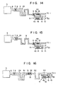
- this invention can be reduced so that the aluminum conductive layer 29 may cover the upper surface of the first end 8 of the resistor R and a part of the resistor R directly behind this first end.
- a third embodiment shown in Fig. 15 only a small portion extending from the first end 8 of the resistor R is covered by the aluminium conductive layer 29.
- the protective circuits according to the embodiments shown in Figs. 14 and 15 have a slightly smaller protecting ability than the protective circuit according to the first embodiment shown in Fig. 12. However, they still produce the effect of the present invention. This is because it is the first end 8 of the resistor R near the contact hole 7 closest to the bonding pad 5 that receives a high voltage having a sharp peak value.
- a polycrystalline silicon resistor R1 having a relatively low resistance is connected between the contact holes 7 and 31, contact holes 31 and 32 are connected by means of the aluminium wire 19, and the contact hole 32 and the drain diffusion layer 4a of the MOS transistor 4 are connected by a resistor R2 constituted by a diffusion layer.
- the whole upper surface of the polycrystalline silicon resistor R1 is covered by the aluminium conductive layer 29.
- the resistor R1 may be covered by the aluminium conductive layer 29, the first end 8 and the part of the resistor R1 directly behind the first end 8 may be covered by the aluminium conductive layer 29, as shown in Fig.
- Figs. 12, 14 and 15 and the resistor R1 of Fig. 16 have been described as being formed of polycrystalline silicon. Instead of these resistors, however, a resistor formed of MoSi2, Mo, or W may be provided within the insulation layer.
- the kind of semiconductor device which can be protected in the above-mentioned way is not limited to MOS integrated circuits, but may be bipolar integrated circuits, or an MOS transistor as a single unit.
- the above-mentioned embodiments of Figs. 12 to 16 can be reduced without modifying the process steps for manufacturing the body of a semiconductor device, adding a process step or steps to such process steps, or enlarging the chip size.
Landscapes
- Insulated Gate Type Field-Effect Transistor (AREA)
- Semiconductor Integrated Circuits (AREA)
Claims (6)
- Dispositif à semiconducteur comportant une couche de résistance (R, R₁) ayant une première extrémité (8) qui reçoit un signal d'entrée en provenance de l'extérieur et une seconde extrémité connectée à un élément semiconducteur, la couche de résistance (R, R₁) étant prévue à l'intérieur d'une couche d'isolation (28) située sur un substrat semiconducteur (SUB), dans lequel le dispositif à semiconducteur comprend une couche conductrice (29) qui recouvre de manière isolante au moins la première extrémité (8) de la couche de résistance (R, R₁) et qui est connectée à la première extrémité (8) au travers d'un trou de contact (30), caractérisé en ce que la couche conductrice (29) recouvre de manière isolante soit la totalité de la couche de résistance (R, R₁), soit une partie de la couche de résistance (R, R₁) qui s'étend depuis la première extrémité (8) de celle-ci de telle sorte que la partie de bord (29a) de la couche conductrice (29) s'étende au-dessus de la partie de bord (20a) de la couche de résistance (R, R₁) afin d'atténuer l'intensité d'un champ électrique produit à l'intérieur de la couche d'isolation (28) au niveau de la partie de bord de la couche de résistance (R, R₁).
- Dispositif à semiconducteur selon la revendication 1, caractérisé en ce que la couche conductrice (29) est connectée à un plot de soudure (5) destiné à l'application du signal d'entrée sur la première extrémité (8).
- Dispositif à semiconducteur selon la revendication 1 ou 2, caractérisé en ce que la couche conductrice (29) est réalisée en aluminium.
- Dispositif à semiconducteur selon l'une quelconque des revendications 1 à 3, caractérisé en ce que la couche de résistance (R, R₁) est réalisée en silicium polycristallin.
- Dispositif à semiconducteur selon l'une quelconque des revendications 1 à 4, caractérisé en ce que la couche conductrice (29) recouvre de manière isolante les bords (20a) de la première extrémité (8) de la couche de résistance (R, R₁).
- Dispositif à semiconducteur selon l'une quelconque des revendications 1 à 4, caractérisé en ce que la couche conductrice (29) recouvre de manière isolante la partie qui correspond à la demi-longueur de la couche de résistance (R, R₁).
Applications Claiming Priority (4)
| Application Number | Priority Date | Filing Date | Title |
|---|---|---|---|
| JP57027023A JPS58143561A (ja) | 1982-02-22 | 1982-02-22 | 半導体装置 |
| JP27023/82 | 1982-02-22 | ||
| JP64684/82 | 1982-04-20 | ||
| JP57064684A JPS58182271A (ja) | 1982-04-20 | 1982-04-20 | 半導体装置 |
Publications (3)
| Publication Number | Publication Date |
|---|---|
| EP0087155A2 EP0087155A2 (fr) | 1983-08-31 |
| EP0087155A3 EP0087155A3 (en) | 1986-08-20 |
| EP0087155B1 true EP0087155B1 (fr) | 1991-05-29 |
Family
ID=26364889
Family Applications (1)
| Application Number | Title | Priority Date | Filing Date |
|---|---|---|---|
| EP83101657A Expired EP0087155B1 (fr) | 1982-02-22 | 1983-02-21 | Moyens pour éviter le claquage d'une couche d'isolation dans un dispositif semi-conducteur |
Country Status (3)
| Country | Link |
|---|---|
| US (1) | US5113230A (fr) |
| EP (1) | EP0087155B1 (fr) |
| DE (1) | DE3382294D1 (fr) |
Families Citing this family (5)
| Publication number | Priority date | Publication date | Assignee | Title |
|---|---|---|---|---|
| FR2635411A1 (fr) * | 1988-08-11 | 1990-02-16 | Sgs Thomson Microelectronics | Memoire de type eprom a haute densite d'integration avec une organisation en damier, un facteur de couplage ameliore et une possibilite de redondance |
| US5268589A (en) * | 1990-09-28 | 1993-12-07 | Siemens Aktiengesellschaft | Semiconductor chip having at least one electrical resistor means |
| EP0598146A1 (fr) * | 1992-11-16 | 1994-05-25 | ALCATEL BELL Naamloze Vennootschap | Dispositif de protection contre des décharges électrostatiques |
| TW344130B (en) | 1995-10-11 | 1998-11-01 | Int Rectifier Corp | Termination structure for semiconductor device and process for its manufacture |
| US5940721A (en) * | 1995-10-11 | 1999-08-17 | International Rectifier Corporation | Termination structure for semiconductor devices and process for manufacture thereof |
Family Cites Families (14)
| Publication number | Priority date | Publication date | Assignee | Title |
|---|---|---|---|---|
| US3518506A (en) * | 1967-12-06 | 1970-06-30 | Ibm | Semiconductor device with contact metallurgy thereon,and method for making same |
| US3862017A (en) * | 1970-02-04 | 1975-01-21 | Hideo Tsunemitsu | Method for producing a thin film passive circuit element |
| JPS5928992B2 (ja) * | 1975-02-14 | 1984-07-17 | 日本電信電話株式会社 | Mosトランジスタおよびその製造方法 |
| JPS5275987A (en) * | 1975-12-22 | 1977-06-25 | Hitachi Ltd | Gate protecting device |
| JPS5299786A (en) * | 1976-02-18 | 1977-08-22 | Agency Of Ind Science & Technol | Mos integrated circuit |
| JPS54137286A (en) * | 1978-04-17 | 1979-10-24 | Nec Corp | Semiconductor device |
| CA1142271A (fr) * | 1979-03-28 | 1983-03-01 | Thomas E. Hendrickson | Semiconducteur a effet de champ |
| US4288806A (en) * | 1979-05-29 | 1981-09-08 | Xerox Corporation | High voltage MOSFET with overlapping electrode structure |
| JPS5811750B2 (ja) * | 1979-06-04 | 1983-03-04 | 株式会社日立製作所 | 高耐圧抵抗素子 |
| JPS5651874A (en) * | 1979-10-05 | 1981-05-09 | Nec Corp | Semiconductor device |
| JPS5852347B2 (ja) * | 1980-02-04 | 1983-11-22 | 株式会社日立製作所 | 高耐圧半導体装置 |
| JPS56169368A (en) * | 1980-05-30 | 1981-12-26 | Sharp Corp | High withstand voltage mos field effect semiconductor device |
| JPS5724563A (en) * | 1980-07-21 | 1982-02-09 | Nec Corp | Semiconductor device |
| US4424579A (en) * | 1981-02-23 | 1984-01-03 | Burroughs Corporation | Mask programmable read-only memory stacked above a semiconductor substrate |
-
1983
- 1983-02-21 EP EP83101657A patent/EP0087155B1/fr not_active Expired
- 1983-02-21 DE DE8383101657T patent/DE3382294D1/de not_active Expired - Lifetime
-
1990
- 1990-08-08 US US07/565,215 patent/US5113230A/en not_active Expired - Lifetime
Also Published As
| Publication number | Publication date |
|---|---|
| EP0087155A3 (en) | 1986-08-20 |
| EP0087155A2 (fr) | 1983-08-31 |
| DE3382294D1 (de) | 1991-07-04 |
| US5113230A (en) | 1992-05-12 |
Similar Documents
| Publication | Publication Date | Title |
|---|---|---|
| EP0161983B1 (fr) | Dispositif de protection d'entrée pour circuit à très grande échelle d'intégration | |
| US4926243A (en) | High voltage MOS field effect semiconductor device | |
| US4057844A (en) | MOS input protection structure | |
| US4481521A (en) | Insulated gate field effect transistor provided with a protective device for a gate insulating film | |
| EP0215493B1 (fr) | Circuit à transistors MOS protégé | |
| JP3217336B2 (ja) | 半導体装置 | |
| US4739438A (en) | Integrated circuit with an improved input protective device | |
| US5019883A (en) | Input protective apparatus of semiconductor device | |
| EP0109070B1 (fr) | Dispositif semi-conducteur du type MOS | |
| EP0087155B1 (fr) | Moyens pour éviter le claquage d'une couche d'isolation dans un dispositif semi-conducteur | |
| US4990984A (en) | Semiconductor device having protective element | |
| JP2541518B2 (ja) | 半導体集積回路装置 | |
| US5532899A (en) | Voltage protection structure for semiconductor devices | |
| JPH0228266B2 (fr) | ||
| EP0083699A2 (fr) | Circuit de protection pour dispositifs semi-conducteurs | |
| JPS6221018Y2 (fr) | ||
| EP0198468A2 (fr) | Dispositif de protection pour circuit intégré | |
| JP3185723B2 (ja) | 半導体装置 | |
| US5432369A (en) | Input/output protection circuit | |
| JPH07147384A (ja) | 半導体装置 | |
| JPH0590522A (ja) | 半導体装置 | |
| JPS60107865A (ja) | Mos型半導体装置 | |
| JPS6355871B2 (fr) | ||
| JPH0518467B2 (fr) | ||
| JPH0518468B2 (fr) |
Legal Events
| Date | Code | Title | Description |
|---|---|---|---|
| PUAI | Public reference made under article 153(3) epc to a published international application that has entered the european phase |
Free format text: ORIGINAL CODE: 0009012 |
|
| 17P | Request for examination filed |
Effective date: 19830319 |
|
| AK | Designated contracting states |
Designated state(s): DE FR GB IT |
|
| RAP1 | Party data changed (applicant data changed or rights of an application transferred) |
Owner name: KABUSHIKI KAISHA TOSHIBA |
|
| PUAL | Search report despatched |
Free format text: ORIGINAL CODE: 0009013 |
|
| RHK1 | Main classification (correction) |
Ipc: H01L 29/60 |
|
| AK | Designated contracting states |
Kind code of ref document: A3 Designated state(s): DE FR GB IT |
|
| 17Q | First examination report despatched |
Effective date: 19880307 |
|
| GRAA | (expected) grant |
Free format text: ORIGINAL CODE: 0009210 |
|
| AK | Designated contracting states |
Kind code of ref document: B1 Designated state(s): DE FR GB IT |
|
| ITF | It: translation for a ep patent filed | ||
| REF | Corresponds to: |
Ref document number: 3382294 Country of ref document: DE Date of ref document: 19910704 |
|
| ET | Fr: translation filed | ||
| PLBE | No opposition filed within time limit |
Free format text: ORIGINAL CODE: 0009261 |
|
| STAA | Information on the status of an ep patent application or granted ep patent |
Free format text: STATUS: NO OPPOSITION FILED WITHIN TIME LIMIT |
|
| 26N | No opposition filed | ||
| PGFP | Annual fee paid to national office [announced via postgrant information from national office to epo] |
Ref country code: FR Payment date: 19970211 Year of fee payment: 15 |
|
| PGFP | Annual fee paid to national office [announced via postgrant information from national office to epo] |
Ref country code: GB Payment date: 19970212 Year of fee payment: 15 |
|
| PGFP | Annual fee paid to national office [announced via postgrant information from national office to epo] |
Ref country code: DE Payment date: 19970228 Year of fee payment: 15 |
|
| PG25 | Lapsed in a contracting state [announced via postgrant information from national office to epo] |
Ref country code: GB Free format text: LAPSE BECAUSE OF NON-PAYMENT OF DUE FEES Effective date: 19980221 |
|
| PG25 | Lapsed in a contracting state [announced via postgrant information from national office to epo] |
Ref country code: FR Free format text: THE PATENT HAS BEEN ANNULLED BY A DECISION OF A NATIONAL AUTHORITY Effective date: 19980228 |
|
| GBPC | Gb: european patent ceased through non-payment of renewal fee |
Effective date: 19980221 |
|
| PG25 | Lapsed in a contracting state [announced via postgrant information from national office to epo] |
Ref country code: DE Free format text: LAPSE BECAUSE OF NON-PAYMENT OF DUE FEES Effective date: 19981103 |
|
| REG | Reference to a national code |
Ref country code: FR Ref legal event code: ST |