EP0087767A2 - Stroboskopisches Rasterelektronenmikroskop - Google Patents
Stroboskopisches Rasterelektronenmikroskop Download PDFInfo
- Publication number
- EP0087767A2 EP0087767A2 EP83101823A EP83101823A EP0087767A2 EP 0087767 A2 EP0087767 A2 EP 0087767A2 EP 83101823 A EP83101823 A EP 83101823A EP 83101823 A EP83101823 A EP 83101823A EP 0087767 A2 EP0087767 A2 EP 0087767A2
- Authority
- EP
- European Patent Office
- Prior art keywords
- axis
- scanning
- counting
- signal
- supplying
- Prior art date
- Legal status (The legal status is an assumption and is not a legal conclusion. Google has not performed a legal analysis and makes no representation as to the accuracy of the status listed.)
- Granted
Links
- 238000010894 electron beam technology Methods 0.000 claims description 48
- 230000001276 controlling effect Effects 0.000 description 6
- 238000010586 diagram Methods 0.000 description 4
- 230000001105 regulatory effect Effects 0.000 description 4
- 206010047571 Visual impairment Diseases 0.000 description 3
- 238000005259 measurement Methods 0.000 description 3
- 230000001360 synchronised effect Effects 0.000 description 3
- 230000003247 decreasing effect Effects 0.000 description 2
- 230000000694 effects Effects 0.000 description 2
- 230000004044 response Effects 0.000 description 2
- 238000004904 shortening Methods 0.000 description 2
- 230000002411 adverse Effects 0.000 description 1
- 230000000593 degrading effect Effects 0.000 description 1
- 238000006073 displacement reaction Methods 0.000 description 1
- 230000005855 radiation Effects 0.000 description 1
Images


Classifications
-
- H—ELECTRICITY
- H01—ELECTRIC ELEMENTS
- H01J—ELECTRIC DISCHARGE TUBES OR DISCHARGE LAMPS
- H01J37/00—Discharge tubes with provision for introducing objects or material to be exposed to the discharge, e.g. for the purpose of examination or processing thereof
- H01J37/26—Electron or ion microscopes; Electron or ion diffraction tubes
- H01J37/266—Measurement of magnetic or electric fields in the object; Lorentzmicroscopy
- H01J37/268—Measurement of magnetic or electric fields in the object; Lorentzmicroscopy with scanning beams
Definitions
- the present invention relates to a stroboscopic scanning electron microscope.
- the stroboscopic scanning electron microscope utilizes a combination of the voltage contrast phenomenon and stroboscopic principles.
- the internal circuits of the LSI are synchronously operated in accordance with a synchronizing signal ⁇ .
- a secondary electron signal indicates the surface potential at the phase ⁇ 1.
- the potential distribution of the LSI at the phase ⁇ 1 can be displayed as an image.
- Fig. 2 shows a conventional stroboscopic scanning electron microscope.
- reference numeral 11 denotes a stroboscopic scanning electron microscope which has a beam pulse generator 12; 13, an LSI as the object to be measured; 14, a tester for supplying a test signal to the LSI 13; and 15, a beam pulse generating circuit for controlling the beam pulse generator 12.
- An electron beam 10 is generated by the beam pulse generating circuit 15 in synchronism with a synchronizing signal SYNC from the tester 14.
- Reference numeral 16 denotes a secondary electron detector which comprises, for example, a scintillator and a photo-multiplier; 17, a CRT display unit for displaying with an image contrast the number of secondary electrons detected by the secondary electron detector 16; 18, a D/A converter for supplying a scanning control signal S X to an X-axis scanning coil 19 through a changeover switch Sl to deflect the electron beam 10, thereby scanning the object with the electron beam 10 along the X-axis; 20, a D/A converter for supplying a scanning control signal S Y to a Y-axis scanning coil 21 through the changeover switch Sl to deflect the electron beam 10, thereby determining the position of the beam spot of the electron beam 10 along the Y-axis; 22, a frequency divider for frequency- dividing the clock signal from the D/A converter 18; and 23 and 24, variable constant-battery circuits, DC voltage signals which are respectively supplied to the X- and Y-axis scanning coils 19 and 21 through the changeover switch S
- a test signal is supplied from the tester 14 to the LSI 13 which is then operated.
- a synchronizing signal SYNC corresponding to the test signal is supplied from the tester 14 to the LSI 13.
- the synchronizing signal SYNC is also supplied to the beam pulse generating circuit 15.
- the beam pulse generator 12 is also controlled by an output from the beam pulse generating circuit 15. As a result, an electron beam 10 which has a period corresponding to the period of the synchronizing signal SYNC is radiated from the beam pulse generator 12 onto the LSI 13.
- the position of the LSI 13 which corresponds to the beam spot of the electron beam 10 is determined by the X- and Y-axis scanning coils 19 and 21.
- the X-axis scanning coil 19 is controlled by the scanning control signal Sx from the D/A converter 18.
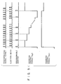
- the output from the D/A converter 18 has a stepwise waveform one step of which- corresponds to one pixel, as shown in Fig. 3.
- the Y-axis scanning coil 21 is controlled by the scanning control signal Sy from the D/A converter 20.
- the scanning control signals Sx and Sy are not synchronized with the electron beams 10.
- the number of pulses of the electron beams 10 varies at different positions of the LSI 13 radiated therewith. For example, three electron beams are radiated onto the LSI 13 during the period of a scanning control signal Sx l , whereas four electron beams are radiated thereonto during the period of a scanning control signal S X2 .
- the corresponding numbers of secondary electrons for corresponding pixels differ. As a result, the measuring precision of the potential distribution on the LSI 13 is degraded.
- Two observation modes are included in the observation of the LSI 13 to be described below.
- a pulsed electron beam is positioned on the desired node of the LSI 13, and a voltage waveform at the surface point of the LSI 13 is displayed by an oscilloscope.
- the first observation mode is called a waveform mode.
- an electron beam is scanned over the desired area of the LSI 13, and the number of secondary electrons from the LSI 13 is visually displayed on a CRT so as to show potential contrast images of the LSI obtained at a desired phase.
- the second observation mode is called an image mode using an SEM (scanning electron microscope). In the conventional stroboscopic scanning electron microscope shown in Fig.
- the secondary electron signal from the LSI 13 is detected by the secondary electron detector 16.
- An output from the secondary electron detector 16 is then supplied as an analog signal to the CRT display unit 17.
- the numbers of secondary electrons are displayed corresponding to the phases of voltage signal from the LSI, thereby obtaining potential contrast images.
- the changeover switch Sl is operated to apply voltages preset by the variable regulated power supplies 23 and 24 to the X- and Y-axis scanning coils 19 and 21, respectively.
- the position onto which the electron beam 10 is radiated is determined by the voltages preset by the variable regulated power supplies 23 and 24.
- the surface of the LSI 13 is scanned with the electron beam 10 to display the secondary electron image on the CRT display unit 17. Thereafter, the changeover switch Sl is switched to set the waveform mode.
- the spot 25 on the CRT display unit 17 is moved to detect a desired observation point. It should be noted that an image 26 remains as an afterimage even if the image display state is changed to spot radiation since the CRT display unit 17 has an afterimage effect. For this reason, the spot 25 is moved while the observer is observing the image 26, so that the electron beam 10 can be radiated onto the desired position of the surface of the LSI 13.
- a stroboscopic scanning electron microscope which comprises: a scanning electron microscope having a beam pulse generator for emitting a pulsed electron beam onto an object to be measured; test signal supplying means for supplying a test signal to the object; beam pulse generating means for controlling said beam pulse generator in response to a synchronous signal from said test signal supplying means; scanning controlling means for controlling scanning by the electron beam from said beam pulse generator; detecting means for detecting the number of secondary electrons generated from the object upon focusing of the electron beam thereonto; displaying means for displaying an output from said detecting means; and display controlling means for controlling said display means.
- the electron beam can be positioned on the observation point with high precision. Furthermore, the electron beam is not radiated onto the object while the observation point is being selected, thereby decreasing the influence of the electron beam on the object. In addition to the advantages described above, a plurality of observation points can be simultaneously selected, thus shortening the measuring time.
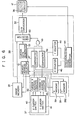
- Figs. 4A and 4B show a stroboscopic scanning electron microscope according to an embodiment of the present invention.
- a synchronizing signal SYNC from a tester 14 is counted down by a programmable counter 31.
- An output from the programmable counter 31 is supplied to a D/A converter 18 through an AND circuit 204 and an X counter 202.
- An output from the programmable counter 31 is also supplied to a frequency divider 22.
- a scanning control section 33 comprises D/A converters 18 and 20, a Y counter 201, the X counter 202, AND gates 203 and 204, the frequency divider 22, the programmable counter 31 and an interface circuit 32.
- a scanning control signal Sx can be synchronized with the synchronizing signal SYNC.
- the count of the programmable counter 31 is preset to be "4"
- the synchronizing signal SYNC is frequency-divided by 1/4.
- a beam pulse generator 12 then produces four pulses of electron beam 10 for every scanning control signal SX .
- the number of pulses of the electron beam 10 is determined by the preset count of the programmable counter 31 which is preset by a pulse number setting signal PC.
- the number of pulses of the electron beam 10 emitted from the beam pulse generator 12 for every step of the scanning control signal Sx can be kept constant by the programmable counter 31.
- the number of pulses of the electron beam 10 emitted from one pixel can be preset to be constant, thus improving the measurement precision.
- an LSI 13 is two-dimensionally scanned with the electron beams 10.
- the number of secondary electrons from the LSI 13 is detected by a secondary electron detector 16.
- a secondary electron signal from the secondary electron detector 16 is supplied to an A/D converter 34 to be converted by the A/D converter 34 to a digital signal.
- the secondary electron signal in the digital form from the A/D converter 34 is stored in an image memory 35.
- the secondary electron signal is read out from the image memory 35 as needed and is displayed at a CRT display unit 17.
- the number of pixels in the image memory 35 corresponds to that of scanning lines at the CRT display unit 17, and also to the number of steps of the scanning control signal having a stepwise waveform. Furthermore, the steps of scanning control signal respectively correspond to the pixels of the image memory 35 in one-to-one correspondence.
- a cross-shaped cursor 36 and an image 26 are displayed on the screen at the CRT display unit 17. The position of the cursor 36 is changed by a controller 37.
- a case for observing a voltage waveform at a given position which is included in the surface of the LSI 13 and which is displayed at the CRT display unit 17 will be described.
- the observer moves the cursor 36 to a position of the screen at the CRT display unit 17 so as to observe a voltage waveform at this position.
- An address of the image memory 35 which corresponds to a pixel at which the cursor 36 is positioned is read by an address reader 38.
- the address of the image memory 35 which corresponds to this pixel is stored in an address memory 39.
- the address memory 39 stores a plurality of addresses of the image memory 35. It should be noted that the addresses of the image memory 35 respectively correspond to the pixels on the screen in one-to-one correspondence.
- the address data stored in the address memory 39 is supplied to the scanning control section 33.
- the D/A converter 18 supplies the scanning control signal Sx to the X-axis scanning coil 19.
- the D/A converter 20 supplies the scanning control signal Sy to the Y-axis scanning coil 21.
- the electron beam 10 is then directed to a position of the surface of the LSI 13 which is specified by the cursor 36 at the CRT display unit 17.
- the interface circuit 32, the address reader 38 and the address memory 39 are controlled by a CPU (central processing unit) 401.
- Fig. 6 is a detailed block diagram showing the CRT display unit 17, the image memory 35, the controller 37, the address reader 38, and the address memory 39.
- reference numeral 40 denotes an X-axis cursor switch; 41, a Y-axis cursor switch.
- the X- and Y-axis cursor switches 40 and 41 are operated to move the cursor 36 displayed at the CRT display unit 17 along the X- and Y-axis, respectively.
- Amounts of displacement of the cursor 36 along the X- and Y-axis are counted by cursor X and Y address counters 42 and 43, respectively.
- cursor X and Y address counters 42 and 43 are counted by cursor X and Y address counters 42 and 43, respectively.
- Reference numeral 44 denotes a synchronizing signal generator for generating horizontal and vertical synchronizing signals H D and V D for image display.
- the horizontal and vertical synchronizing signals H D and V D are supplied to X and Y counters 45 and 46, respectively.
- a vertical synchronizing signal V D is generated every time 512 horizontal synchronizing signals H D are generated, as shown in Fig. 7.
- the screen of the CRT display unit 17 is scanned.
- Outputs from the cursor X address counter 42 and the X counter 45 are supplied to and are compared by an X comparator 47.
- outputs from the cursor Y address counter 43 and the Y counter 46 are supplied to and are compared by a Y comparator 48.
- Outputs from the X and Y comparators 47 and 48 are supplied to a data selector 50 through an AND gate 49.
- the outputs from the X and Y counters 45 and 46 are also supplied to a memory address selector 51.
- the memory address selector 51 sequentially produces a scanning signal to access the image memory 35.
- the secondary electron signal is read out from the image memory 35.
- the read-out signal is supplied to the CRT display unit 17 through the data selector 50 and a D/A converter 52 and is displayed at the CRT display unit 17.
- the AND gate 49 produces a signal of logic level "1".
- cursor display data (e.g., white cross-shaped cursor data) stored in a cursor data generator 53 is supplied to the CRT display unit 17 through the data selector 50 and the D/A converter 52 and is then displayed at the CRT display unit 17.
- the cursor 36 is displayed at a position corresponding to the X and Y addresses respectively accessed by the X- and Y-axis cursor switches 40 and 41.
- the address data which indicates the measuring position specified by the cursor 36 are stored in the address memory 39. More particularly, the count of the cursor X address counter 42 is stored in an X memory 391, and the count of the cursor Y address counter 43 is stored in a Y memory 392.
- the data stored in the X memory 391 is set in the X counter 202, and the data stored in the Y memory 392 is set in the Y counter 201.
- the D/A converter 18 then supplies the scanning control signal S X to the X-axis scanning coil 19, and the D/A converter 20 supplies the scanning control signal Sy to the Y-axis scanning coil 21.
- the electron beam 10 emitted from the beam pulse generator 12 is positioned on the measuring position specified by the cursor 36.
Landscapes
- Chemical & Material Sciences (AREA)
- Analytical Chemistry (AREA)
- Tests Of Electronic Circuits (AREA)
- Testing Or Measuring Of Semiconductors Or The Like (AREA)
Applications Claiming Priority (4)
| Application Number | Priority Date | Filing Date | Title |
|---|---|---|---|
| JP30593/82 | 1982-03-01 | ||
| JP57030593A JPS58150256A (ja) | 1982-03-01 | 1982-03-01 | ストロボ走査型電子顕微鏡装置 |
| JP57109525A JPS59840A (ja) | 1982-06-25 | 1982-06-25 | ストロボ走査型電子顕微鏡装置 |
| JP109525/82 | 1982-06-25 |
Publications (3)
| Publication Number | Publication Date |
|---|---|
| EP0087767A2 true EP0087767A2 (de) | 1983-09-07 |
| EP0087767A3 EP0087767A3 (en) | 1985-05-15 |
| EP0087767B1 EP0087767B1 (de) | 1988-01-20 |
Family
ID=26368976
Family Applications (1)
| Application Number | Title | Priority Date | Filing Date |
|---|---|---|---|
| EP83101823A Expired EP0087767B1 (de) | 1982-03-01 | 1983-02-24 | Stroboskopisches Rasterelektronenmikroskop |
Country Status (3)
| Country | Link |
|---|---|
| US (1) | US4538065A (de) |
| EP (1) | EP0087767B1 (de) |
| DE (1) | DE3375438D1 (de) |
Families Citing this family (6)
| Publication number | Priority date | Publication date | Assignee | Title |
|---|---|---|---|---|
| DE3407041A1 (de) * | 1984-02-27 | 1985-09-05 | Siemens AG, 1000 Berlin und 8000 München | Verfahren zur automatischen einstellung des arbeitspunktes bei signalverlaufsmessungen mit korpuskularstrahl-messgeraeten |
| DE3437550A1 (de) * | 1984-10-12 | 1986-04-24 | Siemens AG, 1000 Berlin und 8000 München | Verfahren zur fehleranalyse an integrierten schaltungen |
| DE3531129A1 (de) * | 1985-08-30 | 1987-03-12 | Siemens Ag | Verfahren und anordnung zum betrieb eines rastermikroskopes |
| KR20190090710A (ko) * | 2018-01-25 | 2019-08-02 | 에프이아이 컴파니 | 하전 입자 빔을 사용하여 집적 회로 내의 고속 전기적 활성을 측정하는 방법 및 장치 |
| US11127562B1 (en) * | 2020-08-05 | 2021-09-21 | Fei Company | System and method for RF pulsed electron beam based STEM |
| EP4246551A1 (de) | 2022-03-14 | 2023-09-20 | Jeol Ltd. | Ladungsteilchenstrahlvorrichtung und steuerungsverfahren für ladungsteilchenstrahlvorrichtung |
Family Cites Families (6)
| Publication number | Priority date | Publication date | Assignee | Title |
|---|---|---|---|---|
| US3535516A (en) * | 1966-10-17 | 1970-10-20 | Hitachi Ltd | Electron microscope employing a modulated scanning beam and a phase sensitive detector to improve the signal to noise ratio |
| GB1286454A (en) * | 1968-08-24 | 1972-08-23 | Cambridge Scientific Instr Ltd | Surface potential analysis by electron beams |
| DE2813948A1 (de) * | 1978-03-31 | 1979-10-11 | Siemens Ag | Verfahren zur elektronischen abbildung der potentialverteilung in einem elektronischen bauelement |
| DE2814049A1 (de) * | 1978-03-31 | 1979-10-18 | Siemens Ag | Verfahren zur beruehrungslosen messung des potentialverlaufs in einem elektronischen bauelement und anordnung zur durchfuehrung des verfahrens |
| DE2813947C2 (de) * | 1978-03-31 | 1986-09-04 | Siemens AG, 1000 Berlin und 8000 München | Verfahren zur berührungslosen Messung des Potentialverlaufs in einem elektronischen Bauelement und Anordnung zur Durchführung des Verfahrens |
| DE3036660A1 (de) * | 1980-09-29 | 1982-05-19 | Siemens AG, 1000 Berlin und 8000 München | Anordnung fuer stroboskopische potentialmessungen mit einem elektronenstrahl-messgeraet |
-
1983
- 1983-02-24 EP EP83101823A patent/EP0087767B1/de not_active Expired
- 1983-02-24 DE DE8383101823T patent/DE3375438D1/de not_active Expired
- 1983-02-28 US US06/470,632 patent/US4538065A/en not_active Expired - Lifetime
Also Published As
| Publication number | Publication date |
|---|---|
| US4538065A (en) | 1985-08-27 |
| EP0087767B1 (de) | 1988-01-20 |
| EP0087767A3 (en) | 1985-05-15 |
| DE3375438D1 (en) | 1988-02-25 |
Similar Documents
| Publication | Publication Date | Title |
|---|---|---|
| US4223220A (en) | Method for electronically imaging the potential distribution in an electronic component and arrangement for implementing the method | |
| US4567364A (en) | Method and apparatus for measuring dimension of secondary electron emission object | |
| US4220853A (en) | Method for the contactless measurement of the potential waveform in an electronic component and arrangement for implementing the method | |
| US4801873A (en) | Waveform measuring apparatus with marker zone displaying function | |
| CA1196416A (en) | Video test method and apparatus with incremental scan rate capability | |
| US4538065A (en) | Stroboscopic scanning electron microscope | |
| US4385317A (en) | Specimen image display apparatus | |
| CA1138115A (en) | Waveform digitizer | |
| EP0123381A1 (de) | Gerät zur Wiedergabe logischer Daten | |
| US7288763B2 (en) | Method of measurement accuracy improvement by control of pattern shrinkage | |
| US3909610A (en) | Apparatus for displaying the energy distribution of a charged particle beam | |
| US5334911A (en) | Apparatus for and method of measuring beam spot luminescence distribution | |
| JP2564359B2 (ja) | パタ−ン検査方法及びパタ−ン測長方法並びに検査装置 | |
| US3354392A (en) | Cathode ray voltmeter using sweep signal for scale generation and for input signal level comparison | |
| JP2010040803A (ja) | 電子ビームを用いた半導体検査装置 | |
| JPS6145549A (ja) | 荷電粒子線装置 | |
| JPS58150256A (ja) | ストロボ走査型電子顕微鏡装置 | |
| JPS61220261A (ja) | 試料表面の対象区域をわき立たせる方法と装置 | |
| JPS5918554A (ja) | 走査型電子顕微鏡の電子ビ−ム位置決め制御装置 | |
| JP2002131018A (ja) | レーザ光線を用いた非接触高さ測定方法 | |
| JP7290747B2 (ja) | 走査電子顕微鏡 | |
| KR20020072279A (ko) | 프로젝션 디스플레이 장치에서의 자동 수렴 방법 | |
| JPH05259239A (ja) | 電子ビーム装置 | |
| JPS6316683B2 (de) | ||
| SU746623A1 (ru) | Устройство дл отображени информации на экране электронно-лучевой трубки |
Legal Events
| Date | Code | Title | Description |
|---|---|---|---|
| PUAI | Public reference made under article 153(3) epc to a published international application that has entered the european phase |
Free format text: ORIGINAL CODE: 0009012 |
|
| 17P | Request for examination filed |
Effective date: 19830321 |
|
| AK | Designated contracting states |
Designated state(s): DE FR GB NL |
|
| RAP1 | Party data changed (applicant data changed or rights of an application transferred) |
Owner name: KABUSHIKI KAISHA TOSHIBA |
|
| PUAL | Search report despatched |
Free format text: ORIGINAL CODE: 0009013 |
|
| AK | Designated contracting states |
Designated state(s): DE FR GB NL |
|
| 17Q | First examination report despatched |
Effective date: 19861007 |
|
| GRAA | (expected) grant |
Free format text: ORIGINAL CODE: 0009210 |
|
| AK | Designated contracting states |
Kind code of ref document: B1 Designated state(s): DE FR GB NL |
|
| REF | Corresponds to: |
Ref document number: 3375438 Country of ref document: DE Date of ref document: 19880225 |
|
| ET | Fr: translation filed | ||
| PLBE | No opposition filed within time limit |
Free format text: ORIGINAL CODE: 0009261 |
|
| STAA | Information on the status of an ep patent application or granted ep patent |
Free format text: STATUS: NO OPPOSITION FILED WITHIN TIME LIMIT |
|
| 26N | No opposition filed | ||
| REG | Reference to a national code |
Ref country code: GB Ref legal event code: 746 Effective date: 19981116 |
|
| REG | Reference to a national code |
Ref country code: FR Ref legal event code: D6 |
|
| REG | Reference to a national code |
Ref country code: FR Ref legal event code: ER Free format text: ERRATUM: LICENCE OF RIGHT ACCEPTED |
|
| REG | Reference to a national code |
Ref country code: FR Ref legal event code: D6 |
|
| REG | Reference to a national code |
Ref country code: GB Ref legal event code: IF02 |
|
| PGFP | Annual fee paid to national office [announced via postgrant information from national office to epo] |
Ref country code: FR Payment date: 20020212 Year of fee payment: 20 |
|
| PGFP | Annual fee paid to national office [announced via postgrant information from national office to epo] |
Ref country code: GB Payment date: 20020227 Year of fee payment: 20 |
|
| PGFP | Annual fee paid to national office [announced via postgrant information from national office to epo] |
Ref country code: NL Payment date: 20020228 Year of fee payment: 20 |
|
| PGFP | Annual fee paid to national office [announced via postgrant information from national office to epo] |
Ref country code: DE Payment date: 20020314 Year of fee payment: 20 |
|
| PG25 | Lapsed in a contracting state [announced via postgrant information from national office to epo] |
Ref country code: GB Free format text: LAPSE BECAUSE OF EXPIRATION OF PROTECTION Effective date: 20030223 |
|
| PG25 | Lapsed in a contracting state [announced via postgrant information from national office to epo] |
Ref country code: NL Free format text: LAPSE BECAUSE OF EXPIRATION OF PROTECTION Effective date: 20030224 |
|
| REG | Reference to a national code |
Ref country code: GB Ref legal event code: PE20 Effective date: 20030223 |
|
| NLV7 | Nl: ceased due to reaching the maximum lifetime of a patent |
Effective date: 20030224 |