EP0087776A2 - Procédé et dispositif pour augmenter la durée de vie et le rendement des dispositifs photovoltaiques à film mince - Google Patents
Procédé et dispositif pour augmenter la durée de vie et le rendement des dispositifs photovoltaiques à film mince Download PDFInfo
- Publication number
- EP0087776A2 EP0087776A2 EP83101862A EP83101862A EP0087776A2 EP 0087776 A2 EP0087776 A2 EP 0087776A2 EP 83101862 A EP83101862 A EP 83101862A EP 83101862 A EP83101862 A EP 83101862A EP 0087776 A2 EP0087776 A2 EP 0087776A2
- Authority
- EP
- European Patent Office
- Prior art keywords
- defect
- semiconductor layer
- laser
- scanning
- eliminating
- Prior art date
- Legal status (The legal status is an assumption and is not a legal conclusion. Google has not performed a legal analysis and makes no representation as to the accuracy of the status listed.)
- Granted
Links
- 239000010409 thin film Substances 0.000 title claims abstract description 25
- 238000000034 method Methods 0.000 title claims abstract description 19
- 230000007547 defect Effects 0.000 claims abstract description 99
- 239000004065 semiconductor Substances 0.000 claims abstract description 82
- 239000000758 substrate Substances 0.000 claims description 38
- 239000000463 material Substances 0.000 claims description 24
- 238000004519 manufacturing process Methods 0.000 claims description 18
- 238000009434 installation Methods 0.000 claims 5
- 210000004027 cell Anatomy 0.000 claims 3
- 210000003850 cellular structure Anatomy 0.000 claims 1
- 238000001514 detection method Methods 0.000 abstract description 6
- 229910052980 cadmium sulfide Inorganic materials 0.000 description 25
- 239000010949 copper Substances 0.000 description 23
- 239000011701 zinc Substances 0.000 description 14
- 230000008030 elimination Effects 0.000 description 11
- 238000003379 elimination reaction Methods 0.000 description 11
- RYGMFSIKBFXOCR-UHFFFAOYSA-N Copper Chemical compound [Cu] RYGMFSIKBFXOCR-UHFFFAOYSA-N 0.000 description 7
- 229910021417 amorphous silicon Inorganic materials 0.000 description 7
- OMZSGWSJDCOLKM-UHFFFAOYSA-N copper(II) sulfide Chemical compound [S-2].[Cu+2] OMZSGWSJDCOLKM-UHFFFAOYSA-N 0.000 description 7
- 239000011521 glass Substances 0.000 description 7
- 238000010586 diagram Methods 0.000 description 6
- HCHKCACWOHOZIP-UHFFFAOYSA-N Zinc Chemical compound [Zn] HCHKCACWOHOZIP-UHFFFAOYSA-N 0.000 description 5
- 239000011888 foil Substances 0.000 description 5
- 239000002184 metal Substances 0.000 description 5
- 229910052751 metal Inorganic materials 0.000 description 5
- 229910052725 zinc Inorganic materials 0.000 description 5
- 239000002131 composite material Substances 0.000 description 4
- 229910052802 copper Inorganic materials 0.000 description 4
- 230000000875 corresponding effect Effects 0.000 description 4
- WUPHOULIZUERAE-UHFFFAOYSA-N 3-(oxolan-2-yl)propanoic acid Chemical compound OC(=O)CCC1CCCO1 WUPHOULIZUERAE-UHFFFAOYSA-N 0.000 description 3
- OKTJSMMVPCPJKN-UHFFFAOYSA-N Carbon Chemical compound [C] OKTJSMMVPCPJKN-UHFFFAOYSA-N 0.000 description 3
- 240000008881 Oenanthe javanica Species 0.000 description 3
- 230000000903 blocking effect Effects 0.000 description 3
- 230000015556 catabolic process Effects 0.000 description 3
- 239000011889 copper foil Substances 0.000 description 3
- 238000006731 degradation reaction Methods 0.000 description 3
- 239000010408 film Substances 0.000 description 3
- 239000010439 graphite Substances 0.000 description 3
- 229910002804 graphite Inorganic materials 0.000 description 3
- 238000001465 metallisation Methods 0.000 description 3
- 229910021420 polycrystalline silicon Inorganic materials 0.000 description 3
- 230000008569 process Effects 0.000 description 3
- 238000012545 processing Methods 0.000 description 3
- 230000005855 radiation Effects 0.000 description 3
- XOLBLPGZBRYERU-UHFFFAOYSA-N tin dioxide Chemical compound O=[Sn]=O XOLBLPGZBRYERU-UHFFFAOYSA-N 0.000 description 3
- 229910001887 tin oxide Inorganic materials 0.000 description 3
- 241000206607 Porphyra umbilicalis Species 0.000 description 2
- 239000000919 ceramic Substances 0.000 description 2
- 238000006243 chemical reaction Methods 0.000 description 2
- 238000000576 coating method Methods 0.000 description 2
- 230000003750 conditioning effect Effects 0.000 description 2
- 239000004020 conductor Substances 0.000 description 2
- 238000000354 decomposition reaction Methods 0.000 description 2
- 238000000151 deposition Methods 0.000 description 2
- 229920001971 elastomer Polymers 0.000 description 2
- 239000000806 elastomer Substances 0.000 description 2
- 230000005611 electricity Effects 0.000 description 2
- 238000010438 heat treatment Methods 0.000 description 2
- 238000002156 mixing Methods 0.000 description 2
- 230000003287 optical effect Effects 0.000 description 2
- 230000009467 reduction Effects 0.000 description 2
- 230000004044 response Effects 0.000 description 2
- 241000283070 Equus zebra Species 0.000 description 1
- 229910001218 Gallium arsenide Inorganic materials 0.000 description 1
- XUIMIQQOPSSXEZ-UHFFFAOYSA-N Silicon Chemical compound [Si] XUIMIQQOPSSXEZ-UHFFFAOYSA-N 0.000 description 1
- 239000006011 Zinc phosphide Substances 0.000 description 1
- 238000005299 abrasion Methods 0.000 description 1
- 230000009471 action Effects 0.000 description 1
- 230000002411 adverse Effects 0.000 description 1
- 230000008901 benefit Effects 0.000 description 1
- 230000015572 biosynthetic process Effects 0.000 description 1
- 239000004568 cement Substances 0.000 description 1
- 239000011195 cermet Substances 0.000 description 1
- 230000008859 change Effects 0.000 description 1
- 239000011248 coating agent Substances 0.000 description 1
- 230000001143 conditioned effect Effects 0.000 description 1
- 238000012790 confirmation Methods 0.000 description 1
- 238000010924 continuous production Methods 0.000 description 1
- HVMJUDPAXRRVQO-UHFFFAOYSA-N copper indium Chemical compound [Cu].[In] HVMJUDPAXRRVQO-UHFFFAOYSA-N 0.000 description 1
- 239000002537 cosmetic Substances 0.000 description 1
- 238000005336 cracking Methods 0.000 description 1
- 230000007423 decrease Effects 0.000 description 1
- 230000008021 deposition Effects 0.000 description 1
- 238000013461 design Methods 0.000 description 1
- 230000000694 effects Effects 0.000 description 1
- 239000008393 encapsulating agent Substances 0.000 description 1
- 238000005530 etching Methods 0.000 description 1
- PCHJSUWPFVWCPO-UHFFFAOYSA-N gold Chemical compound [Au] PCHJSUWPFVWCPO-UHFFFAOYSA-N 0.000 description 1
- CPBQJMYROZQQJC-UHFFFAOYSA-N helium neon Chemical compound [He].[Ne] CPBQJMYROZQQJC-UHFFFAOYSA-N 0.000 description 1
- 238000005286 illumination Methods 0.000 description 1
- 238000010348 incorporation Methods 0.000 description 1
- AMGQUBHHOARCQH-UHFFFAOYSA-N indium;oxotin Chemical compound [In].[Sn]=O AMGQUBHHOARCQH-UHFFFAOYSA-N 0.000 description 1
- 238000013101 initial test Methods 0.000 description 1
- 239000012212 insulator Substances 0.000 description 1
- UGKDIUIOSMUOAW-UHFFFAOYSA-N iron nickel Chemical compound [Fe].[Ni] UGKDIUIOSMUOAW-UHFFFAOYSA-N 0.000 description 1
- 238000007567 mass-production technique Methods 0.000 description 1
- 239000010445 mica Substances 0.000 description 1
- 229910052618 mica group Inorganic materials 0.000 description 1
- 229910021424 microcrystalline silicon Inorganic materials 0.000 description 1
- 239000002245 particle Substances 0.000 description 1
- HOKBIQDJCNTWST-UHFFFAOYSA-N phosphanylidenezinc;zinc Chemical compound [Zn].[Zn]=P.[Zn]=P HOKBIQDJCNTWST-UHFFFAOYSA-N 0.000 description 1
- 229920006254 polymer film Polymers 0.000 description 1
- 229920005591 polysilicon Polymers 0.000 description 1
- 238000010248 power generation Methods 0.000 description 1
- 238000002360 preparation method Methods 0.000 description 1
- 238000012552 review Methods 0.000 description 1
- 229910052710 silicon Inorganic materials 0.000 description 1
- 239000010703 silicon Substances 0.000 description 1
- HBMJWWWQQXIZIP-UHFFFAOYSA-N silicon carbide Chemical compound [Si+]#[C-] HBMJWWWQQXIZIP-UHFFFAOYSA-N 0.000 description 1
- 229910010271 silicon carbide Inorganic materials 0.000 description 1
- 239000007787 solid Substances 0.000 description 1
- 239000007921 spray Substances 0.000 description 1
- 230000000007 visual effect Effects 0.000 description 1
- 229940048462 zinc phosphide Drugs 0.000 description 1
- UQMZPFKLYHOJDL-UHFFFAOYSA-N zinc;cadmium(2+);disulfide Chemical compound [S-2].[S-2].[Zn+2].[Cd+2] UQMZPFKLYHOJDL-UHFFFAOYSA-N 0.000 description 1
Images


Classifications
-
- H—ELECTRICITY
- H10—SEMICONDUCTOR DEVICES; ELECTRIC SOLID-STATE DEVICES NOT OTHERWISE PROVIDED FOR
- H10F—INORGANIC SEMICONDUCTOR DEVICES SENSITIVE TO INFRARED RADIATION, LIGHT, ELECTROMAGNETIC RADIATION OF SHORTER WAVELENGTH OR CORPUSCULAR RADIATION
- H10F71/00—Manufacture or treatment of devices covered by this subclass
-
- H—ELECTRICITY
- H02—GENERATION; CONVERSION OR DISTRIBUTION OF ELECTRIC POWER
- H02S—GENERATION OF ELECTRIC POWER BY CONVERSION OF INFRARED RADIATION, VISIBLE LIGHT OR ULTRAVIOLET LIGHT, e.g. USING PHOTOVOLTAIC [PV] MODULES
- H02S50/00—Monitoring or testing of PV systems, e.g. load balancing or fault identification
- H02S50/10—Testing of PV devices, e.g. of PV modules or single PV cells
-
- Y—GENERAL TAGGING OF NEW TECHNOLOGICAL DEVELOPMENTS; GENERAL TAGGING OF CROSS-SECTIONAL TECHNOLOGIES SPANNING OVER SEVERAL SECTIONS OF THE IPC; TECHNICAL SUBJECTS COVERED BY FORMER USPC CROSS-REFERENCE ART COLLECTIONS [XRACs] AND DIGESTS
- Y02—TECHNOLOGIES OR APPLICATIONS FOR MITIGATION OR ADAPTATION AGAINST CLIMATE CHANGE
- Y02E—REDUCTION OF GREENHOUSE GAS [GHG] EMISSIONS, RELATED TO ENERGY GENERATION, TRANSMISSION OR DISTRIBUTION
- Y02E10/00—Energy generation through renewable energy sources
- Y02E10/50—Photovoltaic [PV] energy
-
- Y—GENERAL TAGGING OF NEW TECHNOLOGICAL DEVELOPMENTS; GENERAL TAGGING OF CROSS-SECTIONAL TECHNOLOGIES SPANNING OVER SEVERAL SECTIONS OF THE IPC; TECHNICAL SUBJECTS COVERED BY FORMER USPC CROSS-REFERENCE ART COLLECTIONS [XRACs] AND DIGESTS
- Y02—TECHNOLOGIES OR APPLICATIONS FOR MITIGATION OR ADAPTATION AGAINST CLIMATE CHANGE
- Y02P—CLIMATE CHANGE MITIGATION TECHNOLOGIES IN THE PRODUCTION OR PROCESSING OF GOODS
- Y02P70/00—Climate change mitigation technologies in the production process for final industrial or consumer products
- Y02P70/50—Manufacturing or production processes characterised by the final manufactured product
Definitions
- the present invention includes as its novelty the use of such scanning equipment, in general, and laser scanners, in particular, in the manner set forth hereinafter, but such laser equipment, per se, and even with thin film photovoltaic cells, is not asserted to be novel.
- NBS Special Publication 400-24, February 1977 by Sawyer and Berning describes a laser scanner for semiconductive devices. Further descriptions of laser scanners are also found in IEEE Transactions on Electron Devices, Vol. ED-27, No. 4, April 1980, pp. 864-872; Solid State Electronics Vol. 23, pp. 565-576, 1979; Proc. SPIE 24th Annual Int'l. Technical Symposium Vol. 248, p p .
- any low resistance electrical path between copper sulfide and the substrate causes electromigration of copper and ultimate electrochemical decomposition of copper sulfide into, inter alia, a nodule or whisker of copper.
- electrochemical decomposition of copper sulfide is recognized as one of the principal factors limiting widespread utilization of copper sulfide comprising photovoltaic cell devices. Elimination of shunting defects in accordance with this invention provides a useful means for obtaining Cu 2 S comprising photovoltaic cells having increased durability and reliability and which heretofore have been unavailable for utilization in photovoltaic ; power generation systems.
- the semiconductor layers are deposited on a large area glass sheet.
- the semiconductor layers are then etched and interconnected in order to form a plurality of strip photovoltaic cells which are electrically connected in a photovoltaic module.
- the prior art has proposed the use of intermediate layers such as an A1 2 O 2 -CdS composite of U.S. Patent 4,159 ,914 in one case and cement buffer layer in another in order to prevent shorts and shunts.
- the present invention provides a superior means for increasing the yield and durability of these types of photovoltaic devices as well.
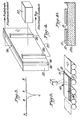
- the manufacturing process involves moving the substrate on a carrier or rollers through the steps of semiconductor deposition and junction formation. After these steps have been completed and prior to metallization, temporary contact is made to the transparent conductive oxide and to the uppermost semiconductor layer. Contact to the transparent conductive oxide is made at exposed edge 17 by a wiper 46 which functions as contact 26 of Figure 4. Contact to the upper surface of semiconductor layers 15 is made by another wiper 48 which functions as contact 20 of Figure 4. Alternatively wiper 48 may be replaced by a contact roller (not shown) functioning as roller 38 of Figure -6 or 7.
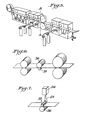
- Laser beam 25 (Fig. 2) is scanned perpendicular to the direction of motion of substrate 12A. Shorts and shunting defects are located and removed in the inventive manner previously described.
- the above invention is particularly advantageous in its manner of precisely locating and then immediately eliminating any shunting defect.
- the invention is also particularly advantageous in that it lends itself to mass production techniques such as continuous manufacture of thin film photovoltiac devices. Accordingly the invention represents a significant advancement for increasing the durability and yield of such devices and may be readily applied to photovoltaic devices comprised of GaAs, or Zn 3 P 2 , or CuInSe 2 , or polycrystalline silicon.
- the above invention is advantageous in precisely locating and eliminating defects which affect the performance, yield and reliability of thin film semiconductor devices such as are useful for electrophotography, radiation detectors and optical displays.
Landscapes
- Photovoltaic Devices (AREA)
Applications Claiming Priority (2)
| Application Number | Priority Date | Filing Date | Title |
|---|---|---|---|
| US35221882A | 1982-02-25 | 1982-02-25 | |
| US352218 | 1982-02-25 |
Publications (3)
| Publication Number | Publication Date |
|---|---|
| EP0087776A2 true EP0087776A2 (fr) | 1983-09-07 |
| EP0087776A3 EP0087776A3 (en) | 1983-10-05 |
| EP0087776B1 EP0087776B1 (fr) | 1987-06-10 |
Family
ID=23384255
Family Applications (1)
| Application Number | Title | Priority Date | Filing Date |
|---|---|---|---|
| EP83101862A Expired EP0087776B1 (fr) | 1982-02-25 | 1983-02-25 | Procédé et dispositif pour augmenter la durée de vie et le rendement des dispositifs photovoltaiques à film mince |
Country Status (4)
| Country | Link |
|---|---|
| EP (1) | EP0087776B1 (fr) |
| JP (1) | JPS58158977A (fr) |
| CA (1) | CA1207069A (fr) |
| DE (1) | DE3372047D1 (fr) |
Cited By (5)
| Publication number | Priority date | Publication date | Assignee | Title |
|---|---|---|---|---|
| EP0179403A3 (fr) * | 1984-10-17 | 1988-08-31 | Fuji Electric Corporate Research And Development Ltd. | Appareil pour la fabrication d'un transducteur photoélectrique à couches minces |
| NL1013204C2 (nl) * | 1999-10-04 | 2001-04-05 | Stichting Energie | Inrichting voor het lokaliseren van productiefouten in een fotovolta´sch element. |
| CN103597739A (zh) * | 2011-03-23 | 2014-02-19 | 帕山股份公司 | 一种用于实现至少一个与至少一个光伏器件可拆卸电接触的系统和方法 |
| WO2018024274A1 (fr) * | 2016-08-02 | 2018-02-08 | Aic Hörmann Gmbh & Co. Kg | Procédé d'amélioration du comportement de contact ohmique entre une grille de contacts et une couche émettrice d'une cellule solaire au silicium |
| US11482630B2 (en) * | 2018-02-07 | 2022-10-25 | Ce Cell Engineering Gmbh | Method for improving the ohmic-contact behaviour between a contact grid and an emitter layer of a silicon solar cell |
Families Citing this family (4)
| Publication number | Priority date | Publication date | Assignee | Title |
|---|---|---|---|---|
| JPS60124882A (ja) * | 1983-12-09 | 1985-07-03 | Agency Of Ind Science & Technol | 太陽電池の製造方法 |
| US20070227586A1 (en) * | 2006-03-31 | 2007-10-04 | Kla-Tencor Technologies Corporation | Detection and ablation of localized shunting defects in photovoltaics |
| EP2159583A1 (fr) * | 2008-08-29 | 2010-03-03 | ODERSUN Aktiengesellschaft | Système et procédé de localisation et de passivation des défauts dans un élément photovoltaïque |
| DE102021132240A1 (de) | 2021-12-08 | 2023-06-15 | Hanwha Q Cells Gmbh | Anlage zur Stabilisierung und/oder Verbesserung eines Wirkungsgrads einer Solarzelle und Verfahren zur Stabilisierung und/oder Verbesserung eines Wirkungsgrads einer Solarzelle |
-
1983
- 1983-02-23 JP JP58027849A patent/JPS58158977A/ja active Granted
- 1983-02-24 CA CA000422343A patent/CA1207069A/fr not_active Expired
- 1983-02-25 DE DE8383101862T patent/DE3372047D1/de not_active Expired
- 1983-02-25 EP EP83101862A patent/EP0087776B1/fr not_active Expired
Non-Patent Citations (4)
| Title |
|---|
| IBM TECHNICAL DISCLOSURE BULLETIN, vol. 19, no. 4, September 1976, pages 1457-1458, New York, USA; J.P. HOEKSTRA: "Testing a multilevel line structure for shorts". * |
| IBM TECHNICAL DISCLOSURE BULLETIN, vol. 24, no. 11B, April 1982, page 6027, New York, USA; S.M. SALEEM et al.: "Contactless electrical isolation detector". * |
| IEEE TRANSACTIONS ON ELECTRON DEVICES, vol. ED-27, no. 4, April 1980, pages 864-872, New York, USA; D.E. SAWYER et al.: "Laser scanning of solar cells for the display of cell operating characteristics and detection of cell defects". * |
| OPTICS & LASER TECHNOLOGY, vol. 12, no. 6, December 1980, pages 317-320, Exeter, GB; "Automatic inspection of silicon wafers". * |
Cited By (11)
| Publication number | Priority date | Publication date | Assignee | Title |
|---|---|---|---|---|
| EP0179403A3 (fr) * | 1984-10-17 | 1988-08-31 | Fuji Electric Corporate Research And Development Ltd. | Appareil pour la fabrication d'un transducteur photoélectrique à couches minces |
| NL1013204C2 (nl) * | 1999-10-04 | 2001-04-05 | Stichting Energie | Inrichting voor het lokaliseren van productiefouten in een fotovolta´sch element. |
| WO2001026163A1 (fr) * | 1999-10-04 | 2001-04-12 | Stichting Energieonderzoek Centrum Nederland | Dispositif permettant de localiser des defauts de fabrication dans un substrat d'element photovoltaique |
| AU772404B2 (en) * | 1999-10-04 | 2004-04-29 | Sunlab B.V. | Apparatus for localizing production errors in a photovoltaic element |
| US6750662B1 (en) | 1999-10-04 | 2004-06-15 | Stichting Energieonderzoek Centrum Nederland | Apparatus for localizing production errors in a photovoltaic element |
| CN103597739A (zh) * | 2011-03-23 | 2014-02-19 | 帕山股份公司 | 一种用于实现至少一个与至少一个光伏器件可拆卸电接触的系统和方法 |
| CN103597739B (zh) * | 2011-03-23 | 2016-12-14 | 帕山股份公司 | 一种用于实现至少一个与至少一个光伏器件可拆卸电接触的系统和方法 |
| WO2018024274A1 (fr) * | 2016-08-02 | 2018-02-08 | Aic Hörmann Gmbh & Co. Kg | Procédé d'amélioration du comportement de contact ohmique entre une grille de contacts et une couche émettrice d'une cellule solaire au silicium |
| US11393944B2 (en) | 2016-08-02 | 2022-07-19 | Ce Cell Engineering Gmbh | Method for improving ohmic contact behaviour between a contact grid and an emitter layer of a silicon solar cell |
| US11482630B2 (en) * | 2018-02-07 | 2022-10-25 | Ce Cell Engineering Gmbh | Method for improving the ohmic-contact behaviour between a contact grid and an emitter layer of a silicon solar cell |
| US11784263B2 (en) | 2018-02-07 | 2023-10-10 | Ce Cell Engineering Gmbh | Method for improving ohmic-contact behaviour between a contact grid and a emitter layer of a silicon solar cell |
Also Published As
| Publication number | Publication date |
|---|---|
| EP0087776B1 (fr) | 1987-06-10 |
| JPH0377672B2 (fr) | 1991-12-11 |
| CA1207069A (fr) | 1986-07-02 |
| DE3372047D1 (en) | 1987-07-16 |
| EP0087776A3 (en) | 1983-10-05 |
| JPS58158977A (ja) | 1983-09-21 |
Similar Documents
| Publication | Publication Date | Title |
|---|---|---|
| US4640002A (en) | Method and apparatus for increasing the durability and yield of thin film photovoltaic devices | |
| US6132585A (en) | Semiconductor element and method and apparatus for fabricating the same | |
| US7979969B2 (en) | Method of detecting and passivating a defect in a solar cell | |
| JP4628628B2 (ja) | 光起電性素子における製造エラーを局所化する装置 | |
| US4292092A (en) | Laser processing technique for fabricating series-connected and tandem junction series-connected solar cells into a solar battery | |
| US4574160A (en) | Flexible, rollable photovoltaic cell module | |
| US6653550B2 (en) | Integrated thin-film photoelectric conversion module | |
| EP0504648B1 (fr) | Batterie de cellules solaires intégrées | |
| EP0213910B1 (fr) | Procédé de fabrication d'un dispositif à semi-conducteur sans courant de fuite à travers une couche semi-conductrice | |
| US8318240B2 (en) | Method and apparatus to remove a segment of a thin film solar cell structure for efficiency improvement | |
| US8318239B2 (en) | Method and apparatus for detecting and passivating defects in thin film solar cells | |
| EP2224495A1 (fr) | Convertisseur photoélectrique à film mince et à couches multiples et son procédé de fabrication | |
| US20200091362A1 (en) | Solar cell module and method for producing same | |
| EP0087776B1 (fr) | Procédé et dispositif pour augmenter la durée de vie et le rendement des dispositifs photovoltaiques à film mince | |
| JP2005515639A (ja) | 薄膜光起電モジュールの製造方法 | |
| JP3078936B2 (ja) | 太陽電池 | |
| Gessert et al. | Grid metallization and antireflection coating optimization for concentrator and one‐sun photovoltaic solar cells | |
| US20240282870A1 (en) | Method for improving the ohmic contact between a front contact grid and a doped layer of a wafer solar cell | |
| Genis et al. | Recent progress in indium tin oxide/polysilicon semiconductor-insulator-semiconductor (SIS) solar cells | |
| Olsen et al. | Investigation of polycrystalline thin film CuInSe/sub 2/cells based on ZnSe windows | |
| Phillips et al. | Simultaneous shunt protection and back contact formation for CdTe solar cells with single wall carbon | |
| JPH06140648A (ja) | 太陽電池及びその製造方法 | |
| Cahen et al. | Overcoming degradation mechanisms in CdTe solar cells: First annual report, August 1998--August 1999 | |
| JPH06204520A (ja) | 太陽電池の欠陥部分封止法 | |
| JPH06204519A (ja) | 太陽電池 |
Legal Events
| Date | Code | Title | Description |
|---|---|---|---|
| PUAI | Public reference made under article 153(3) epc to a published international application that has entered the european phase |
Free format text: ORIGINAL CODE: 0009012 |
|
| PUAL | Search report despatched |
Free format text: ORIGINAL CODE: 0009013 |
|
| AK | Designated contracting states |
Designated state(s): DE FR GB |
|
| AK | Designated contracting states |
Designated state(s): DE FR GB |
|
| 17P | Request for examination filed |
Effective date: 19840405 |
|
| GRAA | (expected) grant |
Free format text: ORIGINAL CODE: 0009210 |
|
| AK | Designated contracting states |
Kind code of ref document: B1 Designated state(s): DE FR GB |
|
| REF | Corresponds to: |
Ref document number: 3372047 Country of ref document: DE Date of ref document: 19870716 |
|
| ET | Fr: translation filed | ||
| PLBE | No opposition filed within time limit |
Free format text: ORIGINAL CODE: 0009261 |
|
| STAA | Information on the status of an ep patent application or granted ep patent |
Free format text: STATUS: NO OPPOSITION FILED WITHIN TIME LIMIT |
|
| 26N | No opposition filed | ||
| PGFP | Annual fee paid to national office [announced via postgrant information from national office to epo] |
Ref country code: FR Payment date: 19910124 Year of fee payment: 9 |
|
| PGFP | Annual fee paid to national office [announced via postgrant information from national office to epo] |
Ref country code: GB Payment date: 19910131 Year of fee payment: 9 |
|
| PGFP | Annual fee paid to national office [announced via postgrant information from national office to epo] |
Ref country code: DE Payment date: 19910227 Year of fee payment: 9 |
|
| PG25 | Lapsed in a contracting state [announced via postgrant information from national office to epo] |
Ref country code: GB Effective date: 19920225 |
|
| GBPC | Gb: european patent ceased through non-payment of renewal fee | ||
| PG25 | Lapsed in a contracting state [announced via postgrant information from national office to epo] |
Ref country code: FR Effective date: 19921030 |
|
| PG25 | Lapsed in a contracting state [announced via postgrant information from national office to epo] |
Ref country code: DE Effective date: 19921103 |
|
| REG | Reference to a national code |
Ref country code: FR Ref legal event code: ST |