EP0088338A1 - Arrangement de convertisseur utilisant des thyristors GTO - Google Patents
Arrangement de convertisseur utilisant des thyristors GTO Download PDFInfo
- Publication number
- EP0088338A1 EP0088338A1 EP83101979A EP83101979A EP0088338A1 EP 0088338 A1 EP0088338 A1 EP 0088338A1 EP 83101979 A EP83101979 A EP 83101979A EP 83101979 A EP83101979 A EP 83101979A EP 0088338 A1 EP0088338 A1 EP 0088338A1
- Authority
- EP
- European Patent Office
- Prior art keywords
- reactors
- gtos
- inverter device
- thyristors
- unit
- Prior art date
- Legal status (The legal status is an assumption and is not a legal conclusion. Google has not performed a legal analysis and makes no representation as to the accuracy of the status listed.)
- Granted
Links
Images


Classifications
-
- H—ELECTRICITY
- H02—GENERATION; CONVERSION OR DISTRIBUTION OF ELECTRIC POWER
- H02M—APPARATUS FOR CONVERSION BETWEEN AC AND AC, BETWEEN AC AND DC, OR BETWEEN DC AND DC, AND FOR USE WITH MAINS OR SIMILAR POWER SUPPLY SYSTEMS; CONVERSION OF DC OR AC INPUT POWER INTO SURGE OUTPUT POWER; CONTROL OR REGULATION THEREOF
- H02M7/00—Conversion of AC power input into DC power output; Conversion of DC power input into AC power output
- H02M7/42—Conversion of DC power input into AC power output without possibility of reversal
- H02M7/44—Conversion of DC power input into AC power output without possibility of reversal by static converters
- H02M7/48—Conversion of DC power input into AC power output without possibility of reversal by static converters using discharge tubes with control electrode or semiconductor devices with control electrode
- H02M7/493—Conversion of DC power input into AC power output without possibility of reversal by static converters using discharge tubes with control electrode or semiconductor devices with control electrode the static converters being arranged for operation in parallel
-
- H—ELECTRICITY
- H02—GENERATION; CONVERSION OR DISTRIBUTION OF ELECTRIC POWER
- H02M—APPARATUS FOR CONVERSION BETWEEN AC AND AC, BETWEEN AC AND DC, OR BETWEEN DC AND DC, AND FOR USE WITH MAINS OR SIMILAR POWER SUPPLY SYSTEMS; CONVERSION OF DC OR AC INPUT POWER INTO SURGE OUTPUT POWER; CONTROL OR REGULATION THEREOF
- H02M7/00—Conversion of AC power input into DC power output; Conversion of DC power input into AC power output
- H02M7/42—Conversion of DC power input into AC power output without possibility of reversal
- H02M7/44—Conversion of DC power input into AC power output without possibility of reversal by static converters
- H02M7/48—Conversion of DC power input into AC power output without possibility of reversal by static converters using discharge tubes with control electrode or semiconductor devices with control electrode
- H02M7/497—Conversion of DC power input into AC power output without possibility of reversal by static converters using discharge tubes with control electrode or semiconductor devices with control electrode sinusoidal output voltages being obtained by combination of several voltages being out of phase
Definitions
- the present relates to an inverter device using gate turn-off thyristors (which will be shortly referred to as "GTO") and, more particularly, to an inverter device which is constructed to have GTOs connected in parallel so as to have its capacity increased.
- GTO gate turn-off thyristors
- An inverter device having parallel-connected GTOs is disclosed, for example, by Takashi Tsuboi and Takamasa Hori in Hitachi Review Vol. 31 (1982), No. 1, pages 23 - 27, "GTO Inverter Controlled AC Traction Drives" and is shown in Fig. 6 of the same.
- a current balancing reactor i.e., a current balancer
- the respective nodes of the positive and negative arms in U, V and W phases provide the a.c. output terminals of that inverter device.
- a leakage inductance exists between the two coils of that current balancing reactor AB.
- an excessive voltage is applied between the anodes and cathodes of those GTOs thereby to invite a fear that the GTOs may be broken.
- a snubber circuit is connected in parallel with a GTO.
- This snubber circuit is constructed by connecting a capacitor C in series with a parallel connection of a resistor R and a diode CR1, as is shown in Figs. 12 and 8 on page 227 of "SILICON CONTROLLED RECTIFIER MANUAL, THIRD EDITION", for example, which was published in 1964 by General Electric Company.
- the snubber circuit is intrinsically provided to suppress an excessive voltage due to the wiring inductance.
- An object of the present invention is to provide an inverter device which can enjoy a high efficiency with a small size by the use of gate turn-off thyristors.
- the gist of the present invention resides in that the arrangement of a current balancing reactor is so.devised that the influence of the reactor may be prevented from being exerted upon the capacitor C of a snubber circuit.
- an inverter device which includes two or more groups of unit switching circuits connected in parallel with a d.c. power source and each having gate turn-off thyristors connected in series with each other such that each group may provide one phase of the inverter device, in which current balancing reactors are respectively connected between the series nodes of the gate turn-off thyristors of the respective groups, and in which respective intermediate points of the reactors provide the a.c. output terminals of the inverter device.
- inverter device constructed of a plurality of unit inverters, on the other hand, there are connected between the corresponding a.c. output terminals of the respective unit inverters current balancing reactors which have their respective intermediate points connected with a load.
- the current balancing reactors are not included in the closed circuit "the power source - the positive arm - the negative arm - the power source", which is established when the GTOs of the respective arms are turned off, so that their leakage inductances do not exert their influences upon the capacitors C of the snubber circuits.
- Fig. 1 is a circuit diagram showing one embodiment of the present invention
- Fig. 2 is a circuit diagram showing a snubber circuit
- Figs. 3 to 5 are circuit diagrams showing other embodiments of the present invention.
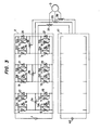
- an inverter device 2 using GTOs operates to convert a d.c. voltage or current, which is supplied from a d.c. power source 1, into an a.c. voltage or current having a desired frequency, which is demanded by a load 3 (e.g., an a.c. electric motor).
- a load 3 e.g., an a.c. electric motor
- the inverter device 2 is composed of six unit switching circuits which are connected in parallel with the d.c. power source 1 and each of which has GTOs connected in series with each other.
- the group which is composed of the unit switching circuit having its GTOs 4 and 6 connected in series and the unit switching circuit having its GTOs 5 and 7 connected in series, provides a U-phase.
- a current balancing reactor 34 which has its intermediate point 0 leading to a U-phase a.c. output terminal.
- the group which is composed-of the unit switching circuit having its GTOs 8 and 10 connected in series and the unit switching circuit having its GTOs 9 and 11 connected in series, provides a V-phase. Between the series node of the GTOs 8 and 10 and the series node of the GTOs 9 and 11, there is connected a current balancing reactor 35, which has its intermediate point leading to a V-phase a.c. output terminal.
- the group which is composed of the unit switching circuit having its GTOs 12 and 14 connected in series and the unit switching circuit having its GTOs 13 and 15 connected in series, provides a W-phase.
- a current balancing reactor 36 which has its intermediate point leading to a W-phase a.c. output terminal.
- Snubber circuits S4 to S15 are respectively connected in parallel with the GTOs 4 to 15 and in anti-parallel with feedback diodes 16 to 27.
- Each of the snubber circuits S4 to S15 is typically composed of a capacitor C, a resistor R and a diode D, as shown in Fig. 2.
- the reactors 35 and 36 act to hold the current balances between the GTOs 8 and.9 and between the-GTOs 10 and 11 and the current balances between the GTOs 12 and 13 and between the GTOs 14 and 15.
- Fig. 3 shows the circuit construction of another embodiment of the present invention.
- a unit inverter 41 which has the same construction as that of the inverter device 2 shown in Fig. 1, and there are connected between the corresponding a.c. output terminals of the two unit, inverters 2 and 41 current balancing reactors 27, 38 and 39 which have their respective intermediate points connected with the load 3.
- a d.c. power source 40 is provided for the unit inverter 41.
- the current balances of the unit inverters 2 and 41 can be ensured by the actions of the reactors 37, 38 and 39, and the influences of those leakage inductances are not exerted upon the capacitors of the snubber circuits likewise the case of Fig. 1.
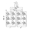
- Fig. 4 shows the circuit construction of still another embodiment of the present invention.
- the group of four unit switching circuits each having GTOs connected in series provides one phase. Only a unit inverter 42 for the U-phase is shown in detail.
- the current balancing reactor 34 is connected between the series node of the GTOs 4 and 6 and the series node of the GTOs 5 and 7, and another current balancing reactor 53 is connected between the series node of the GTOs 45 and 47 and the series node of GTOs 46 and 48.
- still another current balancing reactor 54 which has its intermediate point leading to a U-phase a.c. output terminal.
- unit injectors 43 and 44 for V- and W-phases are made the same as that of the aforementioned U-phase unit injector 42. With these constructions, the currents of the parallel GTOs can be balanced even if the number of the parallel connections of the GTOs increases, and the influences of the leakage inductances of the current balancing reactors are not exerted upon the capacitors of the snubber circuits likewise the embodiment of Fig. 1.
- Fig. 5 shows the circuit construction of a further embodiment of the present invention.
- the present embodiment is constructed of two unit inverters 60 and 62 which have GTOs bridge-connected with one another.
- the d.c. power source 1 is provided for the unit inverter 60, whereas a d.c. power source 63 is provided for the unit inverter 62.
- the current balancing reactors 37, 38 and 39 which have their respective intermediate points connected with the load 3.
- the currents of the unit inverters 60 and 62 can be balanced by the coactions of the reactors 37, 38 and 39, and the influences of the leakage inductances of the reactors 37, 38 and 39 are not exerted upon to the capacitors of the snubber circuits likewise the embodiment of Fig. 1.
- the present invention can be likewise applied not only to the three-phase inverter device but also to a single-phase inverter device and further not only to the voltage type inverter device but also to a current type inverter device.
- the leakage induction components in the coils of the current balancing reactors are made independent of the generation of the excessive voltage, when the respective GTOs are turned off, by the circuit constructions.
- the capacitors of the snubber circuits are sufficient, if they have capacities enough to suppress the excessive voltage due to the wiring inductance components, so that they can have lower capacities than those of the example of the prior art.
- the energy to be consumed by the resistors of the snubber circuits can be reduced, and the efficiency of the device as a whole can be enhanced.
- the capacities of the capacitors of the snubber circuits can be made lower than those of the prior art, moreover, the time period required for charging or discharging those capacitors ean be shortened to increase the number of the pulses in a pulse width modulation (i.e., PWM) control thereby to provide an effect that the elimination of the high-frequency components of the output voltage of the inverter can be enhaned.
- PWM pulse width modulation
Landscapes
- Engineering & Computer Science (AREA)
- Power Engineering (AREA)
- Inverter Devices (AREA)
Applications Claiming Priority (2)
| Application Number | Priority Date | Filing Date | Title |
|---|---|---|---|
| JP57032354A JPS58151877A (ja) | 1982-03-03 | 1982-03-03 | インバ−タ装置 |
| JP32354/82 | 1982-03-03 |
Publications (2)
| Publication Number | Publication Date |
|---|---|
| EP0088338A1 true EP0088338A1 (fr) | 1983-09-14 |
| EP0088338B1 EP0088338B1 (fr) | 1986-08-06 |
Family
ID=12356620
Family Applications (1)
| Application Number | Title | Priority Date | Filing Date |
|---|---|---|---|
| EP83101979A Expired EP0088338B1 (fr) | 1982-03-03 | 1983-03-01 | Arrangement de convertisseur utilisant des thyristors GTO |
Country Status (4)
| Country | Link |
|---|---|
| US (1) | US4549258A (fr) |
| EP (1) | EP0088338B1 (fr) |
| JP (1) | JPS58151877A (fr) |
| DE (1) | DE3365061D1 (fr) |
Cited By (1)
| Publication number | Priority date | Publication date | Assignee | Title |
|---|---|---|---|---|
| WO2013102673A1 (fr) * | 2012-01-06 | 2013-07-11 | Commissariat à l'énergie atomique et aux énergies alternatives | Systeme d'alimentation d'une charge alternative par plusieurs sources de tension continue |
Families Citing this family (14)
| Publication number | Priority date | Publication date | Assignee | Title |
|---|---|---|---|---|
| JPH0815394B2 (ja) * | 1983-10-31 | 1996-02-14 | 株式会社安川電機 | 多重結合インバータ装置の接続・制御方法 |
| JPS63287371A (ja) * | 1987-05-15 | 1988-11-24 | Mitsubishi Electric Corp | 相間リアクトル多重式pwnインバ−タ |
| US4922401A (en) * | 1989-05-22 | 1990-05-01 | International Fuel Cells | Inverter circuit utilizing the reverse voltage capabilities of symmetrical gate turn off thyristors |
| US4992721A (en) * | 1990-01-26 | 1991-02-12 | Sundstrand Corporation | Inverter for starting/generating system |
| US5070440A (en) * | 1990-08-14 | 1991-12-03 | General Electric Company | Power conversion scheme employing paralleled units |
| JP2954333B2 (ja) * | 1990-11-28 | 1999-09-27 | 株式会社日立製作所 | 交流電動機可変速システム |
| US5198971A (en) * | 1991-08-15 | 1993-03-30 | Recker Bradley J | Separation control for multiphase plural inverter system |
| US5434771A (en) * | 1991-09-12 | 1995-07-18 | Sundstrand Corporation | Adaptive harmonic distortion control for parallel connected inverters |
| US5355296A (en) * | 1992-12-10 | 1994-10-11 | Sundstrand Corporation | Switching converter and summing transformer for use therein |
| US5933339A (en) * | 1998-03-23 | 1999-08-03 | Electric Boat Corporation | Modular static power converter connected in a multi-level, multi-phase, multi-circuit configuration |
| US6510063B2 (en) * | 2000-05-30 | 2003-01-21 | Mitsubishi Denki Kabushiki Kaisha | Electric power conversion optimized for efficient harmonic elimination |
| US7138773B2 (en) * | 2003-06-24 | 2006-11-21 | General Electric Company | Multiple inverters for motors |
| NL1030481C2 (nl) * | 2005-11-22 | 2007-05-23 | Atlas Copco Airpower Nv | Inrichting voor aansluiting op een impedantie met een voornamelijk inductief karakter. |
| KR102841013B1 (ko) | 2020-02-03 | 2025-08-01 | 위스크 에어로 엘엘씨 | 에너지 회생 기능을 지니는 차량용 배전 회로 |
Citations (1)
| Publication number | Priority date | Publication date | Assignee | Title |
|---|---|---|---|---|
| DE2103230A1 (de) * | 1971-01-25 | 1972-08-03 | Siemens Ag | Umrichter |
Family Cites Families (8)
| Publication number | Priority date | Publication date | Assignee | Title |
|---|---|---|---|---|
| DE646827C (de) | 1934-06-05 | 1937-06-22 | Aeg | Mehrfachumrichter |
| US2195308A (en) * | 1939-05-06 | 1940-03-26 | Gen Electric | Electric translating system |
| US3386027A (en) * | 1965-09-08 | 1968-05-28 | Westinghouse Electric Corp | High voltage converter apparatus having a plurality of serially connected controllable semiconductor devices |
| GB1371418A (en) | 1972-09-15 | 1974-10-23 | Pioneer Magnetics Inc | Current sharing parallel transistor circuit |
| AT329678B (de) * | 1973-07-13 | 1976-05-25 | Siemens Ag | Schaltungsanordnung bei wechselrichtern |
| JPS5357428A (en) * | 1976-11-04 | 1978-05-24 | Toyo Electric Mfg Co Ltd | Method of suppressing cross current |
| JPS5746679A (en) * | 1980-09-01 | 1982-03-17 | Toshiba Corp | Power converter |
| JPS58141682A (ja) * | 1982-02-16 | 1983-08-23 | Toshiba Corp | 電力変換装置 |
-
1982
- 1982-03-03 JP JP57032354A patent/JPS58151877A/ja active Granted
-
1983
- 1983-03-01 EP EP83101979A patent/EP0088338B1/fr not_active Expired
- 1983-03-01 DE DE8383101979T patent/DE3365061D1/de not_active Expired
- 1983-03-03 US US06/471,704 patent/US4549258A/en not_active Expired - Lifetime
Patent Citations (1)
| Publication number | Priority date | Publication date | Assignee | Title |
|---|---|---|---|---|
| DE2103230A1 (de) * | 1971-01-25 | 1972-08-03 | Siemens Ag | Umrichter |
Non-Patent Citations (3)
| Title |
|---|
| Patent Abstracts of Japan vol. 3, no. 132, 6 November 1979 page 144E149 & JP-A-54-111629 * |
| Patent Abstracts of Japan vol. 5, no. 59, 22 April 1981 & JP-A-56-10079 * |
| Patent Abstracts of Japan vol. 6, no. 87, 25 May 1982 & JP-A-57-22385 (Cat. Y) (published 25.02.1982) * |
Cited By (2)
| Publication number | Priority date | Publication date | Assignee | Title |
|---|---|---|---|---|
| WO2013102673A1 (fr) * | 2012-01-06 | 2013-07-11 | Commissariat à l'énergie atomique et aux énergies alternatives | Systeme d'alimentation d'une charge alternative par plusieurs sources de tension continue |
| FR2985615A1 (fr) * | 2012-01-06 | 2013-07-12 | Commissariat Energie Atomique | Systeme d'alimentation d'une charge alternative par plusieurs sources de tension continue |
Also Published As
| Publication number | Publication date |
|---|---|
| US4549258A (en) | 1985-10-22 |
| DE3365061D1 (en) | 1986-09-11 |
| JPS58151877A (ja) | 1983-09-09 |
| JPH0332304B2 (fr) | 1991-05-10 |
| EP0088338B1 (fr) | 1986-08-06 |
Similar Documents
| Publication | Publication Date | Title |
|---|---|---|
| US9036379B2 (en) | Power converter based on H-bridges | |
| US6072707A (en) | High voltage modular inverter | |
| US9083230B2 (en) | Multilevel voltage source converters and systems | |
| CN100566106C (zh) | 用于切换大数目的切换电压电平的转换器电路 | |
| US4549258A (en) | Inverter device using gate turn-off thyristors | |
| US6977449B2 (en) | Frequency converter and drive for electric motor | |
| US9843270B2 (en) | Phase leg arrangements for multilevel active rectifiers | |
| EP2961057A1 (fr) | Convertisseur de source de tension et commande de celui-ci | |
| CN108476001B (zh) | 四电平功率转换器和三相功率转换器 | |
| US9660553B2 (en) | Switching stage, energy conversion circuit, and conversion stage for wind turbines comprising the energy conversion circuit | |
| CN1072410C (zh) | 半导体功率转换器件 | |
| KR102929978B1 (ko) | 스위칭 커패시터를 구비한 일반화된 멀티레벨 컨버터 회로 토폴로지 | |
| Salari et al. | A novel 49-level asymmetrical modular multilevel inverter: analysis, comparison and validation | |
| JP3160792B2 (ja) | 電力変換装置 | |
| US10608555B2 (en) | Inverter circuit comprising a circuit arrangement for regenerative damping of electrical oscillations, and method for regenerative damping of electrical oscillations | |
| US20240275302A1 (en) | Cell based multilevel converter with multiple operating modes and associated control method | |
| CN110460229B (zh) | 模块化多电平变频器启动电路及其启动与低速运行方法 | |
| EP4641907A1 (fr) | Convertisseur multi-niveaux de condensateur volant | |
| JP3814557B2 (ja) | 半導体電力変換装置 | |
| JP2019193459A (ja) | マルチレベルインバータ | |
| JPH1118413A (ja) | 電力変換装置 | |
| Kim et al. | Three-phase unbalanced-voltage compensators | |
| JPH0698563A (ja) | 電力変換器の制御装置 | |
| JPS6347073B2 (fr) |
Legal Events
| Date | Code | Title | Description |
|---|---|---|---|
| PUAI | Public reference made under article 153(3) epc to a published international application that has entered the european phase |
Free format text: ORIGINAL CODE: 0009012 |
|
| AK | Designated contracting states |
Designated state(s): DE GB |
|
| 17P | Request for examination filed |
Effective date: 19830915 |
|
| GRAA | (expected) grant |
Free format text: ORIGINAL CODE: 0009210 |
|
| AK | Designated contracting states |
Kind code of ref document: B1 Designated state(s): DE GB |
|
| ITF | It: translation for a ep patent filed | ||
| REF | Corresponds to: |
Ref document number: 3365061 Country of ref document: DE Date of ref document: 19860911 |
|
| PLBI | Opposition filed |
Free format text: ORIGINAL CODE: 0009260 |
|
| 26 | Opposition filed |
Opponent name: SIEMENS AKTIENGESELLSCHAFT, BERLIN UND MUENCHEN Effective date: 19870316 |
|
| PGFP | Annual fee paid to national office [announced via postgrant information from national office to epo] |
Ref country code: GB Payment date: 19910221 Year of fee payment: 9 |
|
| PGFP | Annual fee paid to national office [announced via postgrant information from national office to epo] |
Ref country code: DE Payment date: 19910412 Year of fee payment: 9 |
|
| RDAG | Patent revoked |
Free format text: ORIGINAL CODE: 0009271 |
|
| STAA | Information on the status of an ep patent application or granted ep patent |
Free format text: STATUS: PATENT REVOKED |
|
| 27W | Patent revoked |
Effective date: 19910805 |
|
| GBPR | Gb: patent revoked under art. 102 of the ep convention designating the uk as contracting state | ||
| APAC | Appeal dossier modified |
Free format text: ORIGINAL CODE: EPIDOS NOAPO |
|
| APAC | Appeal dossier modified |
Free format text: ORIGINAL CODE: EPIDOS NOAPO |
|
| APAH | Appeal reference modified |
Free format text: ORIGINAL CODE: EPIDOSCREFNO |