EP0088399A2 - Spannungsfester MOS-Transistor für höchstintegrierte Schaltungen - Google Patents
Spannungsfester MOS-Transistor für höchstintegrierte Schaltungen Download PDFInfo
- Publication number
- EP0088399A2 EP0088399A2 EP83102143A EP83102143A EP0088399A2 EP 0088399 A2 EP0088399 A2 EP 0088399A2 EP 83102143 A EP83102143 A EP 83102143A EP 83102143 A EP83102143 A EP 83102143A EP 0088399 A2 EP0088399 A2 EP 0088399A2
- Authority
- EP
- European Patent Office
- Prior art keywords
- conductivity type
- substrate
- mos transistor
- source
- implantation
- Prior art date
- Legal status (The legal status is an assumption and is not a legal conclusion. Google has not performed a legal analysis and makes no representation as to the accuracy of the status listed.)
- Granted
Links
Images

Classifications
-
- H—ELECTRICITY
- H10—SEMICONDUCTOR DEVICES; ELECTRIC SOLID-STATE DEVICES NOT OTHERWISE PROVIDED FOR
- H10D—INORGANIC ELECTRIC SEMICONDUCTOR DEVICES
- H10D62/00—Semiconductor bodies, or regions thereof, of devices having potential barriers
- H10D62/10—Shapes, relative sizes or dispositions of the regions of the semiconductor bodies; Shapes of the semiconductor bodies
- H10D62/17—Semiconductor regions connected to electrodes not carrying current to be rectified, amplified or switched, e.g. channel regions
- H10D62/351—Substrate regions of field-effect devices
- H10D62/357—Substrate regions of field-effect devices of FETs
- H10D62/364—Substrate regions of field-effect devices of FETs of IGFETs
- H10D62/371—Inactive supplementary semiconductor regions, e.g. for preventing punch-through, improving capacity effect or leakage current
-
- H—ELECTRICITY
- H10—SEMICONDUCTOR DEVICES; ELECTRIC SOLID-STATE DEVICES NOT OTHERWISE PROVIDED FOR
- H10D—INORGANIC ELECTRIC SEMICONDUCTOR DEVICES
- H10D30/00—Field-effect transistors [FET]
- H10D30/60—Insulated-gate field-effect transistors [IGFET]
-
- H—ELECTRICITY
- H10—SEMICONDUCTOR DEVICES; ELECTRIC SOLID-STATE DEVICES NOT OTHERWISE PROVIDED FOR
- H10D—INORGANIC ELECTRIC SEMICONDUCTOR DEVICES
- H10D62/00—Semiconductor bodies, or regions thereof, of devices having potential barriers
- H10D62/10—Shapes, relative sizes or dispositions of the regions of the semiconductor bodies; Shapes of the semiconductor bodies
- H10D62/17—Semiconductor regions connected to electrodes not carrying current to be rectified, amplified or switched, e.g. channel regions
- H10D62/213—Channel regions of field-effect devices
- H10D62/221—Channel regions of field-effect devices of FETs
- H10D62/235—Channel regions of field-effect devices of FETs of IGFETs
- H10D62/314—Channel regions of field-effect devices of FETs of IGFETs having vertical doping variations
-
- Y—GENERAL TAGGING OF NEW TECHNOLOGICAL DEVELOPMENTS; GENERAL TAGGING OF CROSS-SECTIONAL TECHNOLOGIES SPANNING OVER SEVERAL SECTIONS OF THE IPC; TECHNICAL SUBJECTS COVERED BY FORMER USPC CROSS-REFERENCE ART COLLECTIONS [XRACs] AND DIGESTS
- Y10—TECHNICAL SUBJECTS COVERED BY FORMER USPC
- Y10S—TECHNICAL SUBJECTS COVERED BY FORMER USPC CROSS-REFERENCE ART COLLECTIONS [XRACs] AND DIGESTS
- Y10S148/00—Metal treatment
- Y10S148/126—Power FETs
Definitions
- the patent application relates to a voltage-proof MOS transistor for highly integrated circuits with a semiconductor substrate of the first conductivity type and an epitaxial layer arranged thereon planar, on the surface of which an insulating layer is arranged and on which a gate electrode made of polysilicon is arranged, and in which extends into the surface area heavily doped source and drain zones of the second conductivity type are generated, and in which a region of the first conductivity type acting as a channel zone is arranged between the source and drain zone, which region has a different concentration of implanted dopant particles in the direction of the substrate, and a method for the same Manufacturing.
- transistors with channel lengths less than 1.5 / um are required, which meet the usual operating voltages of 5 V (- 2.5 V substrate voltage).
- the hole current flowing to the substrate caused a voltage drop. This voltage drop leads to an internal bias of the MOS transistor, which increases the channel current. If the substrate is further increased then the actual bipolar effect occurs.
- the substrate takes on the role of the base of a bipolar transistor, so that an additional current is now injected via the layer sequence corresponding to the emitter, base, and collector, which leads to the breakdown of the MOS transistor.
- the transistor according to the invention suppresses this voltage drop generated by the avalanche multiplication current in that the MOS structure is built up on a low-resistance substrate and a thin, high-resistance epitaxial layer located thereon. This largely eliminates the internal bias or the bipolar effect and thus achieves a higher drain voltage of the MOS transistor.
- the use of an additional implantation mask in the channel implantation reduces the overlap of the channel doping with the source / drain regions and thereby increases the switching speed of the transistor.
- the epitaxial layer realizes the low-doped zone.
- FIGS. 5 and 6 show sections through characteristic transistor areas.
- the better overview is due to adjacent areas of the transistor, such as. B. the illustration of the isolation areas separating the active transistor areas (LOCOS areas) has been omitted.
- Typical implantation parameters for deep implantation are 1 to 3 x 10 12 B cm -2 at 140 keV. With the flat boron implantation and the lower dose, the threshold voltage of the transistor is set in region 8. Typical implantation values are 2 to 6 x 10 11 B cm -2 at 25 keV.
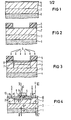
- FIG. 4 shows the transistor structure according to the invention provided with the source / drain and gate connections.
- FIG. 5 shows the concentration profile N A (cm -3 ) along the section line VV 'in FIG. 4 (channel region)
- FIG. 6 shows the concentration profile N A , D (cm -3 ) along the section line VIVI' in FIG. 4 ( Soürce-drain area).
- the individual doping regions (1, 2, 3, 7, 8 and 10) are shown in the diagrams.
- N A and N D mean acceptor or donor concentrations.
- n + substrate capacitance and avalanche-induced bipolar effects are compensated for by the doping regions 1, 2, 3.
- the n + substrate capacity is reduced by the low-doped epitaxial region 2, with a simultaneous increase the breakdown voltage of the pn junction.
- the dashed line in FIG. 6 shows the position of the pn junction.
- the low-resistance regions 1, 3 prevent the internal bias of the transistor and the switching on of the parasitic bipolar transistor. Due to the drop in the dopant concentration between the maximum 11 of the channel implantation and the substrate 1, the substrate control is reduced at high substrate voltages, so that the transistor can also be used as a transfer gate. The extension of the dopant concentration 7 should overlap with the extension of the substrate doping 3 to avoid punch-through effects.
Landscapes
- Insulated Gate Type Field-Effect Transistor (AREA)
- Metal-Oxide And Bipolar Metal-Oxide Semiconductor Integrated Circuits (AREA)
Abstract
Description
- Die Patentanmeldung bezieht sich auf einen spannungsfesten MOS-Transistor für höchstintegrierte Schaltungen mit einem Halbleitersubstrat vom ersten Leitungstyp und einer darauf planar angeordneten epitaktischen Schicht, auf deren Oberfläche eine isolierende Schicht und darauf eine aus Polysilizium bestehende Gateelektrode angeordnet ist, und in der in den Oberflächenbereich hineinreichende stark-dotierte Source- und Drainzonen vom zweiten Leitungstyp erzeugt sind, und in der außerdem zwischen Source- und Drainzone ein als Kanalzone wirkendes Gebiet vom ersten Leitungstyp angeordnet ist, das in Richtung Substrat eine unterschiedliche Konzentration von implantierten Dotierstoffteilchen aufweist, sowie ein Verfahren zu seiner Herstellung.
- Durch die fortschritende Miniaturisierung der integrierten MOS-Schaltungen werden Transistoren mit Kanallängen kleiner 1,5 /um benötigt, welche den üblichen Betriebsspannungen von 5 V (- 2,5 V Substratspannung) genügen. Die daraus resultierende schlechte Reproduzierbarkeit der Einsatzspannung, bedingt durch Kanallängenschwankungen bzw.. eine nicht ausreichende Spannungsfestigkeit infolge Lawinenmultiplikation, gekoppelt mit einem Bipolareffekt, stellt ein schwieriges technisches Problem dar.
- Aus dem Stand der Technik (siehe Aufsatz von R. H. Dennard et al "Design of ion-implanted MOSFET's with very small physical dimensions" in IEEE Sol. State Circuits, Vol. SC-9, Seiten 256 bis 268, 1974) ist es bekannt, dieses Problem dadurch zu lösen, daß ein auf ein hochohmiges Substrat aufgebauter MOS-Transistor im Kanalbereich eine Doppelimplantation enthält und reduzierte Source/Drain-Eindringtiefen sowie ein dünnes Gateoxid aufweist.
- Das Konzept der Doppelimplantation im Kanalbereich, wie es beispielsweise aus einer Arbeit von P. P. Wang aus dem IEEE, ED-24 (1977) auf den Seiten 196 bis 204 zu entnehmen ist, wird in der Praxis nicht voll genützt. Speziell wählt man für die tiefe Implantation eine viel kleinere Dosis als dies für die Abschirmung der Drain- spannung gegenüber'Source optimal wäre, um nicht die Durchbruchsspannungsfestigkeit des Transistors zu reduzieren.
- Andere Konzepte wie doppelt-implantierte MOS-Strukturen, doppelt-diffundierte MOS-Strukturen, MOS-Strukturen mit vergrabenen Zonen, MOS-Strukturen mit getrennten Gates und schwach-dotierten Drain-Zonen sind ebenfalls zur Lösung des Problems bekannt, bringen aber als Nachteil eine größere Komplexität und eine schlechtere Reproduzierbarkeit der Langkanal-Einsatzspannung mit sich.
- Es ist eine Aufgabe der vorliegenden Erfindung, einen MOS-Transistor für höchstintegrierte Schaltungen (Sub-/um-Bereich) anzugeben,-der die Vorteile einer tiefen Implantation mit hoher Dosis auf den Kurzkanaleffekt der Einsatzspannung ausnützt und dabei den Durchbruch des Transistors bei relativ niedrigen Drain-Spannungen vermeidet. Weiter ist es Aufgabe der vorliegenden Erfindung, ein möglichst einfach durchführbares Verfahren zur Herstellung eines wie aufgabengemäß erfundenen MOS-Transistors anzugeben.
- Diese Aufgabe wird durch einen Transistor der eingangs genannten Art gelöst, der erfindungsgemäß gegenüber dem Stand der Technik gekennzeichnet ist durch folgende Merkmale:
- a) Das Substrat vom ersten Leitungstyp ist niederohmig und die epitaktische Schicht ist hochohmig und vom gleichen Leitungstyp wie das Substrat;
- b) die epitaktische Schicht weist eine Schichtdicke auf, die maximal das Zehnfache der Tiefe der Source/Drain- zonen, aber mindestens das Doppelte der Tiefe des Konzentrationsmaximuns der in die Kanalzone implantierten Dotierstoffteilchen, beträgt und
- c) das Kanalgebiet vom ersten Leitungstyp weist in Richtung Substrat eine steigende Dotierstoffkonzentration auf, wobei sich das Konzentrationsmaximum der implantierten Dotierstoffteilchen vom ersten Leitungstyp im Kanalgebiet vom ersten Leitungstyp bis hinter die Source/Drainzone vom zweiten Leitungstyp erstreckt, so, daß das Gebiet mit dem Konzentrationsmaximum der implantierten Dotierstoffteilchen den Rand der Source/Drainzone im Bereich der Gateelektrode umschließt.
- Weitere Ausgestaltungen und Weiterbildungen des Erfindungsgedankens ergeben sich aus den Unteransprüchen.
- Folgende Überlegungen haben zu der Erfindung geführt: Durch den Einfluß der tiefen Implantation wird der Kurzkanaleffekt auf die Einsatzspannung stark reduziert. Bei Untersuchungen des Durchbruchverhaltens wurde festgestellt, daß bei Einsetzen der Lawinenmultiplikation vom Kanalstrom der zum Substrat abfließende Löcherstrom einen Spannungsabfall bewirkt. Dieser Spannungsabfall führt zu einer internen Vorspannung des MOS-Transistors, welche den Kanalstrom erhöht. Bei weiterer Erhöhung des Substratstroms tritt dann der eigentliche Bipolareffekt auf. Dabei übernimmt das Substrat die Rolle der Basis eines Bipolartransistors, so daß über die Schichtfolge nun entsprechend Emitter, Basis, Kollektor ein zusätzlicher Strom injiziert wird, der zum Durchbruch des MOS-Transistors führt.
- Der erfindungsgemäße Transistor unterdrückt diesen vom Lawinenmultiplikationsstrom erzeugten Spannungsabfall dadurch, daß die MOS-Struktur auf niederohmigem Substrat und einer darauf befindlichen, dünnen, hochohmigen Epitaxieschicht aufgebaut wird. Dadurch werden die interne Vorspannung bzw. der Bipolareffekt weitgehend eliminiert und damit eine höhere Drainspannung des MOS-Transistors erreicht. Außerdem wird durch den Einsatz einer zusätzlichen Implantationsmaske bei der Kanalimplantation (vor der Source/Drain-Implantation) die Überlappung der Kanaldotierung mit dem Source/Drain-Gebieten reduziert und dadurch die Schaltgeschwindigkeit des Transistors erhöht. Dabei übernimmt die Epitaxieschicht die Realisierung der niedrig-dotierten Zone.
- Aus der nachfolgenden Beschreibung zu einem bevorzugten Ausführungsbeispiel der Erfindung, das anhand der Figuren gegeben wird, lassen sich weitere Erläuterungen zur Erfindung entnehmen. Dabei zeigen die Figuren 1 bis 4 im Schnittbild den Transistor nach Durchführung der einzelnen Verfahrensschritte und die Figuren 5 und 6 Schnitte durch charakteristische Transistorbereiche. Bei der Darstellung der-Figuren sowie der Beschreibung ist der besseren Übersicht wegen auf benachbarte Bereiche des Transistors, wie z. B. die Darstellung der die aktiven Transistorbereiche trennenden Isolationsbereiche (LOCOS-Gebiete) verzichtet worden.
- Anhand der Figuren 1 bis 4 wird die Herstellung eines n-Kanal-MOS-Transistors beschrieben. Dabei gelten in in allen Figuren für gleiche Teile die gleichen Bezugszeichen.
- Figur 1: Mit 1 ist ein hochdotierter Siliziumsubstratkörper (p++ ≈ 1017 cm-3) von ≈ 500 /um Dicke bezeichnet, auf dessen Oberfläche eins niedriger dotierte epitaktische Siliziumschicht 2 (p- ≈ 1 x 1015 cm-3) in einer Schichtdicke von 2 /um aus der Gasphase niedergeschlagen worden ist. Bei diesem Aufwachsen bildet sich zwischen Substrat 1 und Schicht 2 eine Zwischenschicht durch Diffusion aus dem Substrat 1 aus, die in Figur 1 mit 3 bezeichnet ist. Auf das so beschichtete Substrat (1, 2, 3) wird eine aus Si02 bestehende Isolationsschicht 4 in einer Schichtdicke von kleiner 30 nm aufgewachsen, welche später in bestimmten Bereichen der Schaltung als Gateoxid verwendet wird.
- Figur 2: Auf das mit der Si02-Schicht 4 versehene Substrat (1, 2, 3) wird eine aus Fotolack bestehende Implantationsmaske 5 so aufgebracht, daß die später beim Transistor fungierenden Gatebereiche frei bleiben.
- Figur 3: Mit Hilfe dieser Implantationsmaske 5 wird dann eine Doppelimplantation des Kanalgebietes von aus Bor-Ionen 6 bestehenden Dotierstoffteilchen durchgeführt, wobei die tiefe Implantation (siehe Gebiet 7) gleichzeitig die Feldimplantation erzeugt. Die Verbesserung des Kurzkanaleffekts auf die Einsatzspannung und des Unterschwellenverhaltens wird durch das plateauartige Dotierprofil der Gebiete 7 und 8 erreicht, welches durch die Doppelimplantation 6 erzeugt wird. Das Gebiet 7 mit der hohen Dotierung dient zur Abschirmung des Potentials bei Source an der Oberfläche und im Volumen (SDIBL, VDIBL) gegenüber der Drain-Spannung.
- Typische Implantationsparameter für die tiefe Implantation (Gebiet 7) sind 1 bis 3 x 10¹² B cm-2 bei 140 keV. Mit der flachen Bor-Implantation und niedrigeren Dosis wird im Gebiet 8 die Einsatzspannung des Transistors eingestellt. Typische Implantationswerte sind 2 bis 6 x 10¹¹ B cm-2 bei 25 keV.
- Figur 4: Nach erfolgter Bor-Doppelimplantation 6 wird die Lackmaske 5 entfernt und in bekannter Weise das Polysiliziumgate- und Elektrodenmaterial aufgebracht und die Gateelektrode 9 strukturiert. Unter Verwendung der Gate- elektrode 9 als Implantationsmaske werden dann die Source/Drain-Gebiete 10 mittels einer Arsenimplantation in bekannter Weise erzeugt, wobei für die Tiefe dieser Gebiete ein Bereich von 0,3 bis 0,4 /um eingestellt wird. Wie aus der Figur 4 zu entnehmen ist, liegt das Konzentrationsmaximum (siehe gestrichelte Linie 11) hinter den Source/Draingebieten 10-(im Gegensatz zu der bei Dennard beschriebenen Struktur (Seite 263), in welcher die Source/ Drain-Zonen sich tiefer in das Substrat erstrecken als die tiefe Implantation). Die Figur 4 zeigt die erfindungsgemäße Transistorstruktur mit den Source/Drain- und Gate-Anschlüssen versehen.
- Die Figur 5 zeigt den Konzentrationsverlauf NA (cm-3) entlang der Schnittlinie VV' in Figur 4 (Kanal-Gebiet), die Figur 6 den Konzentrationsverlauf NA,D (cm-3) entlang der Schnittlinie VIVI' in Figur 4 (Soürce-Drain-Gebiet). In den Diagrammen sind die einzelnen Dotierungsgebiete (1, 2, 3, 7, 8 und 10) eingezeichnet. NA und ND bedeuten Akzeptor bzw. Donator-Konzentrationen.
- Die Nachteile der Umkehrung des klassischen Dotierprofils, wie es beispielsweise bei Wang und Dennard beschrieben ist, auf andere Transistoreigenschaften, wie n+-Substrat- kapazität und Avalanche induzierter Bipolareffekte werden durch die Dotierungsgebiete 1, 2, 3 ausgeglichen. Die n+-Substratkapazität wird durch das niedrig dotierte Epitaxiegebiet 2 reduziert, bei gleichzeitiger Erhöhung der Durchbruchsspannung des pn-Überganges. Die gestrichelte Linie in Figur 6 zeigt die Lage des pn-Überganges an. Nach dem heutigen Stand der Technik kann die nicht selbstjustierende Implantationsmaske für den Kanalbereich mit einer Überlappung von 0,5 - 1,0 /um sicher justiert werden.
- Durch die niederohmigen Gebiete 1, 3 wird die interne Vorspannung des Transistors und das Einschalten des parasitären Bipolartransistors verhindert. Durch den Abfall der Dotierstoffkonzentration zwischen dem Maximum 11 der Kanalimplantation und dem Substrat 1 wird die Substratsteuerung bei hohen Substratspannungen reduziert, so daß der Transistor auch als Transfergate verwendet werden kann. Der Ausläufer der Dotierstoff-Konzentration 7 sollte hierbei zur Vermeidung von Punch-Through-Effekten mit dem Ausläufer der Substratdotierung 3 überlappen.
Claims (10)
Priority Applications (1)
| Application Number | Priority Date | Filing Date | Title |
|---|---|---|---|
| AT83102143T ATE35068T1 (de) | 1982-03-09 | 1983-03-04 | Spannungsfester mos-transistor fuer hoechstintegrierte schaltungen. |
Applications Claiming Priority (2)
| Application Number | Priority Date | Filing Date | Title |
|---|---|---|---|
| DE19823208500 DE3208500A1 (de) | 1982-03-09 | 1982-03-09 | Spannungsfester mos-transistor fuer hoechstintegrierte schaltungen |
| DE3208500 | 1982-03-09 |
Publications (3)
| Publication Number | Publication Date |
|---|---|
| EP0088399A2 true EP0088399A2 (de) | 1983-09-14 |
| EP0088399A3 EP0088399A3 (en) | 1986-01-15 |
| EP0088399B1 EP0088399B1 (de) | 1988-06-08 |
Family
ID=6157752
Family Applications (1)
| Application Number | Title | Priority Date | Filing Date |
|---|---|---|---|
| EP83102143A Expired EP0088399B1 (de) | 1982-03-09 | 1983-03-04 | Spannungsfester MOS-Transistor für höchstintegrierte Schaltungen |
Country Status (6)
| Country | Link |
|---|---|
| US (1) | US4966859A (de) |
| EP (1) | EP0088399B1 (de) |
| JP (1) | JPS58165381A (de) |
| AT (1) | ATE35068T1 (de) |
| CA (1) | CA1203321A (de) |
| DE (2) | DE3208500A1 (de) |
Cited By (4)
| Publication number | Priority date | Publication date | Assignee | Title |
|---|---|---|---|---|
| EP0209166A1 (de) * | 1985-06-19 | 1987-01-21 | STMicroelectronics S.r.l. | N-Kanal-MOS-Transistor mit verringertem Durchbruch-Effekt und Verfahren zur Herstellung |
| EP0190935A3 (en) * | 1985-02-08 | 1988-03-02 | Kabushiki Kaisha Toshiba | Method of manufacturing semiconductor devices using a bonding process |
| US4799098A (en) * | 1983-03-28 | 1989-01-17 | Hitachi, Ltd. | MOS/bipolar device with stepped buried layer under active regions |
| EP0434850A4 (en) * | 1989-07-18 | 1991-10-02 | Seiko Instruments Inc. | Semiconductor device |
Families Citing this family (3)
| Publication number | Priority date | Publication date | Assignee | Title |
|---|---|---|---|---|
| US5610429A (en) * | 1994-05-06 | 1997-03-11 | At&T Global Information Solutions Company | Differential analog transistors constructed from digital transistors |
| US5561302A (en) * | 1994-09-26 | 1996-10-01 | Motorola, Inc. | Enhanced mobility MOSFET device and method |
| FR2794898B1 (fr) | 1999-06-11 | 2001-09-14 | France Telecom | Dispositif semi-conducteur a tension de seuil compensee et procede de fabrication |
Family Cites Families (8)
| Publication number | Priority date | Publication date | Assignee | Title |
|---|---|---|---|---|
| GB1153428A (en) * | 1965-06-18 | 1969-05-29 | Philips Nv | Improvements in Semiconductor Devices. |
| JPS5380172A (en) * | 1976-12-25 | 1978-07-15 | Fujitsu Ltd | Semiconductor device |
| JPS5384571A (en) * | 1976-12-29 | 1978-07-26 | Fujitsu Ltd | Insulating gate type field effect transistor and its manufacture |
| JPS5389681A (en) * | 1977-01-19 | 1978-08-07 | Hitachi Ltd | Mis type semiconductor device |
| US4225877A (en) * | 1978-09-05 | 1980-09-30 | Sprague Electric Company | Integrated circuit with C-Mos logic, and a bipolar driver with polysilicon resistors |
| JPS55134974A (en) * | 1979-04-06 | 1980-10-21 | Nec Corp | Manufacturing of semiconductor device |
| JPS5632757A (en) * | 1979-08-25 | 1981-04-02 | Semiconductor Res Found | Insulated gate type transistor and integrated circuit |
| JPS56146276A (en) * | 1980-02-29 | 1981-11-13 | Chiyou Lsi Gijutsu Kenkyu Kumiai | Insulating gate type field-effect transistor |
-
1982
- 1982-03-09 DE DE19823208500 patent/DE3208500A1/de not_active Withdrawn
-
1983
- 1983-03-04 AT AT83102143T patent/ATE35068T1/de not_active IP Right Cessation
- 1983-03-04 DE DE8383102143T patent/DE3377039D1/de not_active Expired
- 1983-03-04 EP EP83102143A patent/EP0088399B1/de not_active Expired
- 1983-03-07 CA CA000423011A patent/CA1203321A/en not_active Expired
- 1983-03-07 JP JP58037216A patent/JPS58165381A/ja active Pending
-
1989
- 1989-01-03 US US07/293,567 patent/US4966859A/en not_active Expired - Lifetime
Non-Patent Citations (4)
| Title |
|---|
| IBM TECHNICAL DISCLOSURE BULLETIN, Band 15, Nr. 10, March 1973, Seiten 3068-3069, New York, US; F. GAENSSLEN: "Ultra-short channel mosfet device" * |
| IBM TECHNICAL DISCLOSURE BULLETIN, Band 15, Nr. 10, Mars 1978, Seiten 4178-4180, New York, US; E.F. MIERSCH et al: "FET structures for very high performance circuits operating at low temperatures" * |
| IEDM 1974 INTERNATIONAL ELECTRON DEVICES MEETING, Nr. 23.6, 9.-11. December 1974, Seiten 550-553, The Institute of Electrical and Electronics Engineers, New York, US; W.S. JOHNSON et al.: "Design of short-channel ion-implanted mosfets with relatively junctions" * |
| IEEE TRANSACTIONS ON ELCTRON DEVICES, Band ED-24, Nr. 3, Mars 1977, Seiten 196-204, New York, US; P.P. WANG: "Double boron implant short-channel MOSFET" * |
Cited By (4)
| Publication number | Priority date | Publication date | Assignee | Title |
|---|---|---|---|---|
| US4799098A (en) * | 1983-03-28 | 1989-01-17 | Hitachi, Ltd. | MOS/bipolar device with stepped buried layer under active regions |
| EP0190935A3 (en) * | 1985-02-08 | 1988-03-02 | Kabushiki Kaisha Toshiba | Method of manufacturing semiconductor devices using a bonding process |
| EP0209166A1 (de) * | 1985-06-19 | 1987-01-21 | STMicroelectronics S.r.l. | N-Kanal-MOS-Transistor mit verringertem Durchbruch-Effekt und Verfahren zur Herstellung |
| EP0434850A4 (en) * | 1989-07-18 | 1991-10-02 | Seiko Instruments Inc. | Semiconductor device |
Also Published As
| Publication number | Publication date |
|---|---|
| EP0088399A3 (en) | 1986-01-15 |
| DE3208500A1 (de) | 1983-09-15 |
| ATE35068T1 (de) | 1988-06-15 |
| JPS58165381A (ja) | 1983-09-30 |
| US4966859A (en) | 1990-10-30 |
| CA1203321A (en) | 1986-04-15 |
| EP0088399B1 (de) | 1988-06-08 |
| DE3377039D1 (en) | 1988-07-14 |
Similar Documents
| Publication | Publication Date | Title |
|---|---|---|
| DE69520782T2 (de) | Randabschlussmethode und Struktur für Leistungs-MOSFET | |
| DE2214935C2 (de) | Integrierte MOS-Schaltung | |
| DE60132994T2 (de) | Verfahren zur herstellung eines leistungs-mosfets | |
| EP0003231B1 (de) | MIS-Feldeffekttransistor mit kurzer Kanallänge und Verfahren zu dessen Herstellung | |
| DE19736981C2 (de) | Halbleitereinrichtung mit hoher Durchbruchsspannung | |
| DE3122768C2 (de) | ||
| DE3853778T2 (de) | Verfahren zur Herstellung eines Halbleiterbauelements. | |
| DE2654482C2 (de) | ||
| DE69505416T2 (de) | Fermi-schwellenspannung-feldeffekttransistor in einer geformten wanne und verfahren zur herstellung | |
| DE19919955A1 (de) | Halbleitervorrichtung mit hoher Spannungsfestigkeit | |
| DE19642538A1 (de) | Halbleitereinrichtung und Herstellungsverfahren derselben | |
| DE68923629T2 (de) | MIS Bauelement mit zusätzlichem Gate. | |
| DE3901369A1 (de) | Verfahren zur herstellung einer doppelt diffundierten metall-oxid-halbleiter-feldeffekt-transistorvorrichtung sowie durch dieses verfahren hergestellte vorrichtung | |
| DE2611338A1 (de) | Feldeffekttransistor mit sehr kurzer kanallaenge | |
| DE3116268C2 (de) | Verfahren zur Herstellung einer Halbleiteranordnung | |
| DE19733974C2 (de) | MOSFET-Einrichtung und Verfahren zur Herstellung | |
| DE3440674A1 (de) | Feldeffekt-transistor | |
| DE19818518C2 (de) | Halbleitervorrichtung und Verfahren zu deren Herstellung | |
| EP0088399B1 (de) | Spannungsfester MOS-Transistor für höchstintegrierte Schaltungen | |
| DE3423776C2 (de) | Verfahren zur Herstellung einer Halbleiteranordnung | |
| DE2729657A1 (de) | Feldeffekttransistor mit extrem kurzer kanallaenge | |
| DE10249009A1 (de) | Halbleitervorrichtung | |
| DE4401470A1 (de) | Eine Bimos-Vorrichtung mit einem bipolaren Transistor und einem Mostriggertransistor und ein Verfahren zu deren Herstellung | |
| DE3787691T2 (de) | MOS-Feldeffekttransistor und Verfahren zu dessen Herstellung. | |
| DE1589891B (de) | Integrierte Halbleiterschaltung |
Legal Events
| Date | Code | Title | Description |
|---|---|---|---|
| PUAI | Public reference made under article 153(3) epc to a published international application that has entered the european phase |
Free format text: ORIGINAL CODE: 0009012 |
|
| AK | Designated contracting states |
Designated state(s): AT BE DE FR GB IT NL SE |
|
| 17P | Request for examination filed |
Effective date: 19841213 |
|
| PUAL | Search report despatched |
Free format text: ORIGINAL CODE: 0009013 |
|
| AK | Designated contracting states |
Designated state(s): AT BE DE FR GB IT NL SE |
|
| 17Q | First examination report despatched |
Effective date: 19871110 |
|
| GRAA | (expected) grant |
Free format text: ORIGINAL CODE: 0009210 |
|
| AK | Designated contracting states |
Kind code of ref document: B1 Designated state(s): AT BE DE FR GB IT NL SE |
|
| REF | Corresponds to: |
Ref document number: 35068 Country of ref document: AT Date of ref document: 19880615 Kind code of ref document: T |
|
| GBT | Gb: translation of ep patent filed (gb section 77(6)(a)/1977) | ||
| REF | Corresponds to: |
Ref document number: 3377039 Country of ref document: DE Date of ref document: 19880714 |
|
| ET | Fr: translation filed | ||
| ITF | It: translation for a ep patent filed | ||
| PLBE | No opposition filed within time limit |
Free format text: ORIGINAL CODE: 0009261 |
|
| STAA | Information on the status of an ep patent application or granted ep patent |
Free format text: STATUS: NO OPPOSITION FILED WITHIN TIME LIMIT |
|
| 26N | No opposition filed | ||
| ITTA | It: last paid annual fee | ||
| EAL | Se: european patent in force in sweden |
Ref document number: 83102143.1 |
|
| PGFP | Annual fee paid to national office [announced via postgrant information from national office to epo] |
Ref country code: AT Payment date: 19970305 Year of fee payment: 15 |
|
| PGFP | Annual fee paid to national office [announced via postgrant information from national office to epo] |
Ref country code: BE Payment date: 19970317 Year of fee payment: 15 |
|
| PGFP | Annual fee paid to national office [announced via postgrant information from national office to epo] |
Ref country code: NL Payment date: 19970320 Year of fee payment: 15 |
|
| PGFP | Annual fee paid to national office [announced via postgrant information from national office to epo] |
Ref country code: SE Payment date: 19970321 Year of fee payment: 15 |
|
| PGFP | Annual fee paid to national office [announced via postgrant information from national office to epo] |
Ref country code: GB Payment date: 19980211 Year of fee payment: 16 |
|
| PG25 | Lapsed in a contracting state [announced via postgrant information from national office to epo] |
Ref country code: AT Free format text: LAPSE BECAUSE OF NON-PAYMENT OF DUE FEES Effective date: 19980304 |
|
| PG25 | Lapsed in a contracting state [announced via postgrant information from national office to epo] |
Ref country code: SE Free format text: LAPSE BECAUSE OF NON-PAYMENT OF DUE FEES Effective date: 19980305 |
|
| PGFP | Annual fee paid to national office [announced via postgrant information from national office to epo] |
Ref country code: FR Payment date: 19980327 Year of fee payment: 16 |
|
| PG25 | Lapsed in a contracting state [announced via postgrant information from national office to epo] |
Ref country code: BE Free format text: LAPSE BECAUSE OF NON-PAYMENT OF DUE FEES Effective date: 19980331 |
|
| BERE | Be: lapsed |
Owner name: SIEMENS A.G. BERLIN UND MUNCHEN Effective date: 19980331 |
|
| PG25 | Lapsed in a contracting state [announced via postgrant information from national office to epo] |
Ref country code: NL Free format text: LAPSE BECAUSE OF NON-PAYMENT OF DUE FEES Effective date: 19981001 |
|
| NLV4 | Nl: lapsed or anulled due to non-payment of the annual fee |
Effective date: 19981001 |
|
| EUG | Se: european patent has lapsed |
Ref document number: 83102143.1 |
|
| PG25 | Lapsed in a contracting state [announced via postgrant information from national office to epo] |
Ref country code: GB Free format text: LAPSE BECAUSE OF NON-PAYMENT OF DUE FEES Effective date: 19990304 |
|
| GBPC | Gb: european patent ceased through non-payment of renewal fee |
Effective date: 19990304 |
|
| PG25 | Lapsed in a contracting state [announced via postgrant information from national office to epo] |
Ref country code: FR Free format text: LAPSE BECAUSE OF NON-PAYMENT OF DUE FEES Effective date: 19991130 |
|
| REG | Reference to a national code |
Ref country code: FR Ref legal event code: ST |
|
| PGFP | Annual fee paid to national office [announced via postgrant information from national office to epo] |
Ref country code: DE Payment date: 20020521 Year of fee payment: 20 |