EP0088967A2 - Verfahren zur Laserbehandlung für Thyristoren zum Selbstschutz gegen Uberspannung - Google Patents
Verfahren zur Laserbehandlung für Thyristoren zum Selbstschutz gegen Uberspannung Download PDFInfo
- Publication number
- EP0088967A2 EP0088967A2 EP83102146A EP83102146A EP0088967A2 EP 0088967 A2 EP0088967 A2 EP 0088967A2 EP 83102146 A EP83102146 A EP 83102146A EP 83102146 A EP83102146 A EP 83102146A EP 0088967 A2 EP0088967 A2 EP 0088967A2
- Authority
- EP
- European Patent Office
- Prior art keywords
- thyristor
- laser radiation
- pulse
- region
- laser
- Prior art date
- Legal status (The legal status is an assumption and is not a legal conclusion. Google has not performed a legal analysis and makes no representation as to the accuracy of the status listed.)
- Granted
Links
Images

Classifications
-
- H—ELECTRICITY
- H10—SEMICONDUCTOR DEVICES; ELECTRIC SOLID-STATE DEVICES NOT OTHERWISE PROVIDED FOR
- H10P—GENERIC PROCESSES OR APPARATUS FOR THE MANUFACTURE OR TREATMENT OF DEVICES COVERED BY CLASS H10
- H10P34/00—Irradiation with electromagnetic or particle radiation of wafers, substrates or parts of devices
- H10P34/40—Irradiation with electromagnetic or particle radiation of wafers, substrates or parts of devices with high-energy radiation
- H10P34/42—Irradiation with electromagnetic or particle radiation of wafers, substrates or parts of devices with high-energy radiation with electromagnetic radiation, e.g. laser annealing
-
- H—ELECTRICITY
- H10—SEMICONDUCTOR DEVICES; ELECTRIC SOLID-STATE DEVICES NOT OTHERWISE PROVIDED FOR
- H10D—INORGANIC ELECTRIC SEMICONDUCTOR DEVICES
- H10D18/00—Thyristors
- H10D18/211—Thyristors having built-in localised breakdown or breakover regions, e.g. self-protected against destructive spontaneous firing
Definitions
- the present invention is generally in the field of power semiconductor devices generally and more specifically related to overvoltage protection of thyristors.
- overvoltage protection of a thyristor employs an avalanche current in the gate region to trigger the thyristor.
- the avalanching is achieved by etching a deep well, approximately 10 mils, in the gate region after an aluminum diffusion and before a gallium diffusion is carried out.
- the avalanche voltage is determined by the depth and profile of the etched well.
- avalanching for self protection will succeed or fail depending on whether the avalanche voltage is less than or more than the edge breakdown voltage of the device.
- avalanching necessarily involves some derating of the electrical parameters of the device. Particularly, there is a derating of the forward blocking voltage, V DRM , along with an attendant increase in forward drop, V F l for the same V DRM.
- a major shortcoming of the etched well protection system is the requirement that the well be formed relatively early in the wafer fabrication processing, before the blocking capability of the thyristor can be measured.
- a deep well that results in avalanching at 2800 volts provides no protection to a thyristor which experiences edge breakdown at 2700 volts.
- a 2800 volt avalanche is too much derating for a thyristor which could block 3200 volts.
- the deep well avalanche method leaves the process engineer the choice between high yield with greatly derated thyristors or a low yield with only slightly derated devices.
- the principal object of the invention is to provide an improved manufacturing process for thyristors.
- the present invention resides broadly in a process for making a thyristor with overvoltage protection comprising the step of: pulsing the general center of a gating region of a thyristor with at least one pulse of laser radiation in order to alter the blocking voltage of said thyristor.
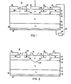
- a thyristor 10 With reference to Fig. 1, there is shown a thyristor 10.
- the thyristor 10 is a typical thyristor known to those skilled in the art.
- the thyristor 10 comprised of silicon has a cathode emitter region 12 which is of N+ type conductivity doped to a concentration of from 10 18 to 5 x10 21 atoms/cc. Typically, the cathode emitter region has a thickness of from 15 to 20 microns.
- the cathode base region 14 is of P type conductivity and doped to a concentration of from 10 15 to 10 17 atoms/cc. Typically, the cathode base region has a thickness of from 70 to 90 microns.
- Adjacent to the cathode emitter base region 14 is an anode base region 18.
- the anode base region 18 is of N type conductivity and doped to a concentration of 13 17 from 10 to 10 17 atoms/cc.
- the thickness of the anode base region is dependent on the breakdown voltage capability desired for the thyristor. Typically, the anode base region will have a thickness of one micron for each 10 volts of breakdown voltage desired.
- Anode emitter region 22 is adjacent to the anode base region 18.
- the anode emitter region 22 is of P+ type conductivity and is doped to a concentration of from 10 18 to 5 x 10 21 atmos/cc.
- the anode base region has a thickness of from 70 to 90 microns.
- auxiliary emitter or floating gate region 26 formed in the cathode base region 14 and spaced apart from the cathode emitter region 12.
- the auxiliary emitter or floating gate region 26 is of N type conductivity and doped to a concentration of from 10 18 to 5x10 21 .
- An aluminum ohmic contact 28, referred to as an emitter contact, is affixed to the cathode emitter contact 12 on top surface 30 of the thyristor 10.
- a second aluminum ohmic contact 32 is affixed to the auxiliary emitter or floating gate region 26 on top surface 30 of the thyristor 10.
- the ohmic contact 32 is in ohmic electrical contact with both the auxiliary emitter region 26 and the cathode base region 14 and bridges the PN junction 29 where the junction 29 intersects surface 30.
- a gate contact 34 is disposed on surface 30 in ohmic electrical contact with cathode base region 14.
- the contacts 28, 32 and 34 all disposed on top surface 30 of the thyristor 10 are spaced apart from each other as shown in Fig. 1.
- An anode emitter contact 36 preferably of molybdenum, is affixed to bottom surface 38 of the thyristor 10 in ohmic electrical contact with the anode emitter region 22.
- Thyristors of the type thus far described are generally edge fired thyristors.
- a curve tracer 40 is electrically connected between the cathode emitter contact 28 and the anode emitter contact 36 by an electrical conductor 42.
- the IV characteristic of the thyristor is measured using the curve tracer.
- a laser is then used to pulse the thyristor 10 at approximately the center of the cathode base region, i.e., the center of the gating region, and the IV characteristic of the thyristor is measured after each pulse to determine the blocking voltage.
- the laser pulsing is continued until the desired blocking voltage is realized.
- the laser used in practicing this invention may be a ruby laser, a C0 2 laser, argon laser or a YAG laser.
- pulse width and energy per pulse are not critical since the pulsing can be repeated until the desired results are achieved.
- thyristor 10 after being pulsed one or more times by the laser.
- the laser pulses have melted the aluminum gate contact 34 and the molten aluminum dissolves some of the silicon and the laser pulse melts some of the silicon.
- the result is that PN junction 20 is driven farther into the body of silicon in the center of the gating region, denoted as 44 in Fig. 2, due to the melting and resolidification of the silicon.
- This reshaping of the PN junction 20 causes the thyristor to undergo avalanche breakdown at voltages slightly less than the surface breakdown voltage.
- the laser pulsing creates a localized weak spot in the gating region of the forward blocking junction, PN junction 20.
- the laser induced weak spot causes the forward blocking junction to break down in the central gating region and the thyristor is protected against an overvoltage.
- the thyristor whose IV characteristic is shown in Figs. 3 and 4 had the configuration shown in Fig. 1.
- the cathode emitter region had a thickness of 15 microns, was of N type conductivity and was doped to a surface concentration of 10 20 atoms/cc.
- the cathode base region had a thickness of 75 microns, was of P type conductivity and was doped to a concentration of 10 17 atoms/cc.
- the anode base region had a thickness of 120 microns, was of N type conductivity and doped to a concen- trationof5xl0 13 at om s/c c .
- the anode emitter region had a thickness of 75 microns, was of P type conductivity and doped to a concentration of 10 17 atoms / cc.
- the thyristor had an auxiliary emitter or floating gate having a thickness of 15 microns, was of N type conductivity and doped to a surface concentration of 10 20 atoms/cc.
- the thyristor was connected to a curve tracer as shown in Fig. 1 and the IV characteristic was measured. The result of this measurement is shown in Fig. 3.
- the device had a forward blocking voltage of approximately 1160 volts.
- the thyristor was then pulsed three times with a ruby laser having a pulse width of 100 micro-seconds and an energy level of 200 milli joules. No change was measured after the first two pulses, however, as shown in Fig. 4, after the third pulse the thyristors forward blocking voltage was reduced to approximately 800 volts.
- the laser pulse causes some melting of the aluminum gate contact 34 is melted by the laser pulse.
- the aluminum contact can also cause some scattering of the laser pulse.
- the thyristor be pulsed with the laser and the gate contact then be affixed.
Landscapes
- Thyristors (AREA)
- Power Conversion In General (AREA)
Applications Claiming Priority (2)
| Application Number | Priority Date | Filing Date | Title |
|---|---|---|---|
| US35710682A | 1982-03-11 | 1982-03-11 | |
| US357106 | 1982-03-11 |
Publications (3)
| Publication Number | Publication Date |
|---|---|
| EP0088967A2 true EP0088967A2 (de) | 1983-09-21 |
| EP0088967A3 EP0088967A3 (en) | 1985-12-27 |
| EP0088967B1 EP0088967B1 (de) | 1987-12-16 |
Family
ID=23404319
Family Applications (1)
| Application Number | Title | Priority Date | Filing Date |
|---|---|---|---|
| EP83102146A Expired EP0088967B1 (de) | 1982-03-11 | 1983-03-04 | Verfahren zur Laserbehandlung für Thyristoren zum Selbstschutz gegen Uberspannung |
Country Status (7)
| Country | Link |
|---|---|
| EP (1) | EP0088967B1 (de) |
| JP (1) | JPS58166767A (de) |
| BR (1) | BR8301120A (de) |
| CA (1) | CA1191974A (de) |
| DE (1) | DE3374972D1 (de) |
| IE (1) | IE54111B1 (de) |
| IN (1) | IN156292B (de) |
Cited By (3)
| Publication number | Priority date | Publication date | Assignee | Title |
|---|---|---|---|---|
| FR2541513A1 (fr) * | 1983-02-18 | 1984-08-24 | Westinghouse Electric Corp | Thyristor auto-protege et son procede de fabrication |
| US4907056A (en) * | 1987-10-08 | 1990-03-06 | Siemens Aktiengesellschaft | Semiconductor component comprising a planar pn-junction |
| EP0572826A1 (de) * | 1992-05-11 | 1993-12-08 | Siemens Aktiengesellschaft | Thyristor mit Durchbruchbereich |
Families Citing this family (1)
| Publication number | Priority date | Publication date | Assignee | Title |
|---|---|---|---|---|
| JPH0680820B2 (ja) * | 1989-10-16 | 1994-10-12 | 株式会社東芝 | 過電圧保護機能付半導体装置及びその製造方法 |
Family Cites Families (5)
| Publication number | Priority date | Publication date | Assignee | Title |
|---|---|---|---|---|
| US4087834A (en) * | 1976-03-22 | 1978-05-02 | General Electric Company | Self-protecting semiconductor device |
| US4075037A (en) * | 1976-05-17 | 1978-02-21 | Westinghouse Electric Corporation | Tailoring of recovery charge in power diodes and thyristors by irradiation |
| DE2928685A1 (de) * | 1978-07-20 | 1980-01-31 | Electric Power Res Inst | Thyristor mit gesteuertem strom bei spannungsdurchbruch und verfahren zur begrenzung des durchbruchstroms in durchlassrichtung durch einen thyristor |
| JPS55115364A (en) * | 1979-02-28 | 1980-09-05 | Nec Corp | Manufacturing method of semiconductor device |
| JPS5643665A (en) * | 1979-09-18 | 1981-04-22 | Minolta Camera Co Ltd | Electrophotographic receptor |
-
1983
- 1983-02-10 IE IE266/83A patent/IE54111B1/en unknown
- 1983-02-14 CA CA000421554A patent/CA1191974A/en not_active Expired
- 1983-02-19 IN IN201/CAL/83A patent/IN156292B/en unknown
- 1983-03-04 EP EP83102146A patent/EP0088967B1/de not_active Expired
- 1983-03-04 DE DE8383102146T patent/DE3374972D1/de not_active Expired
- 1983-03-08 BR BR8301120A patent/BR8301120A/pt unknown
- 1983-03-10 JP JP58038398A patent/JPS58166767A/ja active Pending
Cited By (3)
| Publication number | Priority date | Publication date | Assignee | Title |
|---|---|---|---|---|
| FR2541513A1 (fr) * | 1983-02-18 | 1984-08-24 | Westinghouse Electric Corp | Thyristor auto-protege et son procede de fabrication |
| US4907056A (en) * | 1987-10-08 | 1990-03-06 | Siemens Aktiengesellschaft | Semiconductor component comprising a planar pn-junction |
| EP0572826A1 (de) * | 1992-05-11 | 1993-12-08 | Siemens Aktiengesellschaft | Thyristor mit Durchbruchbereich |
Also Published As
| Publication number | Publication date |
|---|---|
| BR8301120A (pt) | 1983-11-22 |
| CA1191974A (en) | 1985-08-13 |
| EP0088967B1 (de) | 1987-12-16 |
| IE54111B1 (en) | 1989-06-21 |
| JPS58166767A (ja) | 1983-10-01 |
| IN156292B (de) | 1985-06-15 |
| IE830266L (en) | 1983-09-11 |
| DE3374972D1 (en) | 1988-01-28 |
| EP0088967A3 (en) | 1985-12-27 |
Similar Documents
| Publication | Publication Date | Title |
|---|---|---|
| US4240843A (en) | Forming self-guarded p-n junctions by epitaxial regrowth of amorphous regions using selective radiation annealing | |
| US4165517A (en) | Self-protection against breakover turn-on failure in thyristors through selective base lifetime control | |
| US7728409B2 (en) | Semiconductor device and method of manufacturing the same | |
| US3893153A (en) | Light activated thyristor with high di/dt capability | |
| US6043516A (en) | Semiconductor component with scattering centers within a lateral resistor region | |
| EP0125138B1 (de) | Selbstschützender Thyristor und Herstellungsverfahren | |
| US20070048982A1 (en) | Method of manufacturing semiconductor device and semiconductor device formed by the method | |
| US3991460A (en) | Method of making a light activated semiconductor controlled rectifier | |
| EP0088967B1 (de) | Verfahren zur Laserbehandlung für Thyristoren zum Selbstschutz gegen Uberspannung | |
| US4437107A (en) | Self-igniting thyristor with a plurality of discrete, field controlled zener diodes | |
| GB2038551A (en) | Impurity redistribution using radiation or electron beam in semiconductor devices | |
| US4514898A (en) | Method of making a self protected thyristor | |
| EP0106658B1 (de) | Temperaturstabiler selbstschützender Thyristor und Herstellungsverfahren | |
| JP3210013B2 (ja) | 調整可能なブレークオーバ電圧を有するサイリスタおよびその製造方法 | |
| EP0209986A2 (de) | Thyristoren mit Überspannungsschutz | |
| JPWO2018179798A1 (ja) | 半導体装置の製造方法 | |
| JP2003501825A (ja) | リカバリタイム保護機能が集積されたサイリスタ及びその製造方法 | |
| CA1298920C (en) | Protection of thyristors during turn-on | |
| EP0129702A1 (de) | Gegen Fehlzündung geschützter Thyristor mit einer feldbegrenzenden Schicht in der Lawinendurchbruchsspannungszone | |
| US4536783A (en) | High di/dt, light-triggered thyristor with etched moat current limiting resistors | |
| GB1588534A (en) | Protection against voltage breakover turn-on failure in thyristors | |
| CA1097824A (en) | Semiconductor switching device | |
| GB2135515A (en) | Thyristor self-protected by remote punch through | |
| US4611222A (en) | Solid-state switch | |
| JPH04111358A (ja) | 過電圧自己保護型サイリスタ |
Legal Events
| Date | Code | Title | Description |
|---|---|---|---|
| PUAI | Public reference made under article 153(3) epc to a published international application that has entered the european phase |
Free format text: ORIGINAL CODE: 0009012 |
|
| AK | Designated contracting states |
Designated state(s): BE DE FR GB |
|
| 17P | Request for examination filed |
Effective date: 19840217 |
|
| PUAL | Search report despatched |
Free format text: ORIGINAL CODE: 0009013 |
|
| AK | Designated contracting states |
Designated state(s): BE DE FR GB |
|
| 17Q | First examination report despatched |
Effective date: 19870303 |
|
| GRAA | (expected) grant |
Free format text: ORIGINAL CODE: 0009210 |
|
| AK | Designated contracting states |
Kind code of ref document: B1 Designated state(s): BE DE FR GB |
|
| REF | Corresponds to: |
Ref document number: 3374972 Country of ref document: DE Date of ref document: 19880128 |
|
| ET | Fr: translation filed | ||
| PLBE | No opposition filed within time limit |
Free format text: ORIGINAL CODE: 0009261 |
|
| STAA | Information on the status of an ep patent application or granted ep patent |
Free format text: STATUS: NO OPPOSITION FILED WITHIN TIME LIMIT |
|
| 26N | No opposition filed | ||
| PGFP | Annual fee paid to national office [announced via postgrant information from national office to epo] |
Ref country code: BE Payment date: 19910114 Year of fee payment: 9 |
|
| PG25 | Lapsed in a contracting state [announced via postgrant information from national office to epo] |
Ref country code: BE Effective date: 19920331 |
|
| BERE | Be: lapsed |
Owner name: WESTINGHOUSE ELECTRIC CORP. Effective date: 19920331 |
|
| PGFP | Annual fee paid to national office [announced via postgrant information from national office to epo] |
Ref country code: GB Payment date: 19960208 Year of fee payment: 14 |
|
| PGFP | Annual fee paid to national office [announced via postgrant information from national office to epo] |
Ref country code: FR Payment date: 19960307 Year of fee payment: 14 |
|
| PGFP | Annual fee paid to national office [announced via postgrant information from national office to epo] |
Ref country code: DE Payment date: 19960328 Year of fee payment: 14 |
|
| PG25 | Lapsed in a contracting state [announced via postgrant information from national office to epo] |
Ref country code: GB Effective date: 19970304 |
|
| GBPC | Gb: european patent ceased through non-payment of renewal fee |
Effective date: 19970304 |
|
| PG25 | Lapsed in a contracting state [announced via postgrant information from national office to epo] |
Ref country code: FR Free format text: LAPSE BECAUSE OF NON-PAYMENT OF DUE FEES Effective date: 19971128 |
|
| PG25 | Lapsed in a contracting state [announced via postgrant information from national office to epo] |
Ref country code: DE Effective date: 19971202 |
|
| REG | Reference to a national code |
Ref country code: FR Ref legal event code: ST |