EP0089853A2 - Circuit de détection d'ondes d'interférences pour application dans un récepteur radio - Google Patents
Circuit de détection d'ondes d'interférences pour application dans un récepteur radio Download PDFInfo
- Publication number
- EP0089853A2 EP0089853A2 EP83301605A EP83301605A EP0089853A2 EP 0089853 A2 EP0089853 A2 EP 0089853A2 EP 83301605 A EP83301605 A EP 83301605A EP 83301605 A EP83301605 A EP 83301605A EP 0089853 A2 EP0089853 A2 EP 0089853A2
- Authority
- EP
- European Patent Office
- Prior art keywords
- output
- level
- carrier wave
- interference wave
- wave detection
- Prior art date
- Legal status (The legal status is an assumption and is not a legal conclusion. Google has not performed a legal analysis and makes no representation as to the accuracy of the status listed.)
- Granted
Links
Images




Classifications
-
- H—ELECTRICITY
- H04—ELECTRIC COMMUNICATION TECHNIQUE
- H04B—TRANSMISSION
- H04B1/00—Details of transmission systems, not covered by a single one of groups H04B3/00 - H04B13/00; Details of transmission systems not characterised by the medium used for transmission
- H04B1/06—Receivers
- H04B1/10—Means associated with receiver for limiting or suppressing noise or interference
- H04B1/1027—Means associated with receiver for limiting or suppressing noise or interference assessing signal quality or detecting noise/interference for the received signal
Definitions
- This invention relates to a circuit for detecting interference waves received in a radio receiver and, more particularly, to an interference wave detection circuit suitable for use in a mobile radio communication system of multi-frequency access type.
- a plurality of radio concentrators are individually connected to subscriber lines, which are respectively coupled to corresponding radio telephone sets via radio channels. If different frequencies are allotted to respective radio channels, there will be no interference among these channels under normal conditions. In practice, however, to utilize the frequencies more effectively, the radio channels of the adjacent radio zones share the same frequency band. This causes these radio channels to interfere with each other. Such interference provides a beat in the received signals because there is a slight frequency difference in the radio channels of the same frequency. To avoid the beat and establish normal telephone services, the channel concerned has to be switched to another free channel.
- Such switching of the channel is conventionally carried out by manually operating the switch when a subscriber hears beat sounds.
- a subscriber hears beat sounds.
- he has to listen to it for a certain duration of time. This is not only uncomfortable to the subscriber but also is detrimental to the system as the communication over the radio channel has to be suspended for the time period.
- An object of the present invention accordingly is to provide an interference wave detection circuit for accurately detecting the beat caused by the interference between carrier waves of channels.
- Another object of the present invention is to provide an interference wave detection circuit for detecting the above-mentioned beat within a time as short as possible.
- an interference wave detection circuit comprising amplifier means for amplifying a received carrier wave in response to a control signal; amplitude detector means for amplitude-detecting the output from the amplifier means; means for supplying the output of the amplitude detector means to the amplifier means as the control signal so as to make the output level of the amplifier means constant; level measuring means for measuring the level of the output fluctuation of the amplitude detector means; comparator means for comparing the output level of the level measuring means with a predetermined level to provide a compared output as an interference wave detection signal to the output of the interference wave detection circuit; discriminating means connected to the output of the amplifier means for judging whether the received carrier wave is modulated or not; and gate means responsive to the output of the discriminating means for preventing the compared output from reaching the output of the interference wave detection circuit when the discriminating means judges that the received carrier wave is modulated.
- radio concentrators A, B and C are connected respectively to subscriber lines SL A , SL B and SL C .
- SL A , SL B and SL C subscriber lines
- the concentrator C and the radio telephone set C' are to begin the use of the channel at the same time, as both sets of frequencies f l , f l ', and f 2 , f 2 ' are in use, the concentrator C and telephone set C' cannot be connected to each other and they have to wait till either one of the frequencies becomes free.
- the radio concentrator D and the radio telephone set D' belonging to another group may use the frequencies f 1 , f l ' to establish a radio channel. If they are located at places remote enough to avoid interference, no problems will occur. But when the radio telephone set A' moves closer to the radio concentrator D, the radio concentrator D will receive the carrier wave from the radio telephone set A' in addition to that from the radio telephone set D', and mutual interference takes place as mentioned in the foregoing. The radio concentrator D and the radio telephone set D' are then switched to other free frequencies.
- the circuit according to the present invention enables to obtain in shorter time and with a higher accuracy an interference wave detection signal which is necessary for electrically conducting such switching instead of manual switching.
- the difference between the frequencies of these two carrier waves generally appears as a beat in the receiving signal. Since the beat is an envelope signal of the carrier waves, the beat can be amplitude-detected. Precise detection, however, can not be made by merely detecting the receiving signal. Even if phase modulation (PM) or frequency modulation (FM), i.e., angle modulation is adopted to the system, fluctuation will occur not only in phase but in amplitude during conversation. This is because the nonlineary of frequency and/or phase characteristics of the transmission line reduces the amount of phase or frequency modulation and introduces amplitude modulation. This phenomenon is known as PM (or FM)-to-PM conversion.
- PM phase modulation
- FM frequency modulation
- the present invention is conceived based on the above-mentioned points and aims to accurately detect an interference wave, if any.
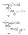
- the output level of an amplifier circuit 1 whose gain is controllable is detected by an amplitude-detector 2.
- the gain of the amplifier circuit 1 is controlled in a manner to make its output level a constant value according to the output of the amplitude-detector 2.
- the output voltage of the amplitude detector 2 acts to lower the gain of the amplifier circuit 1 when the level of the received carrier wave is high and to raise the gain when the level of the received carrier wave is low. Therefore, when the amplitude of the received carrier wave is being fluctuated by the interference waves or the like, beat signal extracted in the amplitude detector 2 suppresses such fluctuation.
- the level of the extracted beat signal is then measured by a level measuring circuit 3, as will be obvious from Figs. 4 and 5.
- the output of the level measuring circuit 3 is compared at a comparator 4 with a reference voltage Vc which is supplied from a potentiometer 18.
- the comparator 4 when the output level of the circuit 3 exceeds the voltage Vc, provides a signal showing that the amplitude fluctuation of the received carrier wave has reached a predetermined value.
- the demodulation output level from a PM (or FM) demodulator 5 becomes high during conversation, the level is detected by a voice level detector 6 to learn whether there is a voice signal or not; in other words whether the carrier is modulated with a voice signal or not.
- the voice level detector 6 detects that there is a voice signal, the output of the comparator 4 is not necessarily raised by interference wave. Accordingly, responsive to the output of the voice level detector 6, a gate circuit 7 prevents erroneous detection of interference waves.
- reference numerals 1 to 6 are identical with those used for Fig. 2, except that the circuit of Fig. 3 is different from that of Fig. 2; an analog gate 8 is incorporated on the input side of the level measuring circuit 3, replacing the gate circuit 7 of Fig. 2. That is, when the voice level detector 6 detects that the carrier wave is modulated, the analog gate 8 is opened even if the output of the amplitude detector 2 fluctuates slightly, so as to prevent the output of the level measuring circuit 3 from rising to avoid erroneous detection of interference waves.
- the beat will effect the phase (or the frequency) of the carrier wave, and the demodulation in PM (or FM) will generate beat sounds, thereby deteriorating the speech quality.
- the D/U ratio widely fluctuates due to fading, the beat sound suddenly becomes louder, and it is necessary to detect the interference wave quickly.
- the interference wave exceeds the desired wave due to fading, i.e., the D/U ratio deteriorates, the demodulation result of the interference wave appears in the PM (or FM) demodulation output, so that crosstalk might be caused. Therefore, a certain precaution described hereinbelow should be taken for the detection of interference waves when there is fading.
- Figs. 4 and 5 show specific structures of the level measuring circuits which have been conceived in order to quickly detect interference waves when a beat have a high level.
- the circuits correspond to the circuit 3 used in Figs. 2 and 3.
- the level measuring circuit shown in Fig. 4 includes a non-linear circuit 10 through which the fluctuation component of high level easily passes, a rectifier circuit 11, a smoothing circuit 12, and a low-pass filter 12.
- the output of the non-linear circuit 10 rises quickly in response to the high level input and, also, the output (OUT) rectified, smoothed and filtered arises quickly. Therefore, when the high level beats are supplied to the non-linear circuit 10, the circuit shown in Fig. 4 can quickly detect them as interference waves.
- the rectifier circuit 11 and the smoothing circuit 12 are identical to those of Fig. 4 except that a non-linear filter 14 is newly added for stabilizing the output of the smoothing circuit 12.
- a non-linear filter 14 is newly added for stabilizing the output of the smoothing circuit 12.
- the filter 14 filters the output of the smoothing circuit 12 with a time constant R 3 C 1 .
- the level measuring circuit shown in Figs. 4 or 5 is thus utilized, even if the beats due to interference waves become larger by fading, the level measuring circuit detects them more quickly thereby preventing the loud beat sound from becoming audible to the subscriber for a long period.
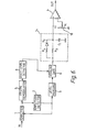
- a non-linear low-pass filter 14 between the output of the analog gate 8 and the input of the comparator 4.
- the filter 14 is structured similarly to the non-linear filter shown in Fig. 5 so as to allow quick enough response to the beats of high level.
- the level measuring circuit 3 may be constructed as shown in Fig. 7 which is identical to the circuit structure shown in Fig. 4 except for the fact that the low-pass filter 13 is omitted.
- an automatic-gain-control (AGC) amplifier circuit 1' is a circuit of the type which can control the gain in respect of the amplitude fluctuation such as fading subsequently but can not control the gain in respect of fast amplitude fluctuation such as beats caused by interference waves is selected.
- AGC automatic-gain-control
- the level measuring circuit 3 measures the level of the beats supplied from the amplitude detector circuit 2'. When the output of the level measuring circuit 3 exceeds the threshold voltage V c ' the comparator 4 judges that the amplitude fluctuation has reached a predetermined value.
- the PM (FM) demodulator circuit 5 for preventing erroneous detection of interference waves, the voice level detector 6 and the gate circuit 7 operate identically to those shown in Fig. 2.
- the analog gate 8 is positioned at the same location and operates in the same way as that of the embodiment shown in Fig. 3.
- the other components are identical to those of Fig. 8 and operate in the same way as the Fig. 8.
- the circuit of Fig. 10 is a modification of the one shown in Fig. 9 except that the analog gate 8 and the amplitude detector 2' are replaced by each other. More specifically, when the voice level detector 6 detects that the carrier wave is modulated, the analog gate 8 becomes blocked to make the output of the amplitude detector 2' constant, thereby preventing the output of the level measuring circuit 3 from rising. Hence, there is no possibility for erroneously detecting the output of the comparator 4 as an interference wave.
- the circuits shown in Figs. 4 and 5 may be used as the level measure circuit 3 in a similar manner to those shown in Figs. 2 and 3 in order to quickly detect the interference wave when beats have a high level.
- the amplifier circuit 1', the amplitude detector 2, PM (FM) demodulator circuit 4 and the voice level detector 5 are identical to those shown in Fig. 8. While the combination of the level measuring circuit 3, the analog gate 8, the low-pass filter 14 and the comparator 4 is the same as the one shown in Fig. 6. These corresponding circuits operate also in a similar manner.
- the circuit shown in Fig. 7 may be used as the level measuring circuit similarly as the embodiment of Fig. 6.
- the circuit according to the present invention enables automatic detection of the fact that an interference occurs from the beats in the carrier wave received by a radio receiver.
- the circuit according to the present invention is especially superior in the response characteristics with respect to the level fluctuation of beats caused by fading and in protection operation against the erroneous detection of interference waves during conversation.
- the circuit according to the present invention is particularly effective when such an automatic frequency switching device is used in combination with a cordless telephone set.
Landscapes
- Engineering & Computer Science (AREA)
- Computer Networks & Wireless Communication (AREA)
- Signal Processing (AREA)
- Noise Elimination (AREA)
- Monitoring And Testing Of Transmission In General (AREA)
Applications Claiming Priority (8)
| Application Number | Priority Date | Filing Date | Title |
|---|---|---|---|
| JP57044673A JPS58162145A (ja) | 1982-03-23 | 1982-03-23 | 干渉波検出方式 |
| JP44671/82 | 1982-03-23 | ||
| JP44672/82 | 1982-03-23 | ||
| JP44673/82 | 1982-03-23 | ||
| JP57044671A JPS58162143A (ja) | 1982-03-23 | 1982-03-23 | 干渉波検出方式 |
| JP57044672A JPS58162144A (ja) | 1982-03-23 | 1982-03-23 | 干渉波検出方式 |
| JP57044674A JPS58162146A (ja) | 1982-03-23 | 1982-03-23 | 干渉波検出方式 |
| JP44674/82 | 1982-03-23 |
Publications (3)
| Publication Number | Publication Date |
|---|---|
| EP0089853A2 true EP0089853A2 (fr) | 1983-09-28 |
| EP0089853A3 EP0089853A3 (en) | 1984-12-12 |
| EP0089853B1 EP0089853B1 (fr) | 1987-04-01 |
Family
ID=27461565
Family Applications (1)
| Application Number | Title | Priority Date | Filing Date |
|---|---|---|---|
| EP83301605A Expired EP0089853B1 (fr) | 1982-03-23 | 1983-03-22 | Circuit de détection d'ondes d'interférences pour application dans un récepteur radio |
Country Status (4)
| Country | Link |
|---|---|
| US (1) | US4525868A (fr) |
| EP (1) | EP0089853B1 (fr) |
| AU (1) | AU555378B2 (fr) |
| CA (1) | CA1196966A (fr) |
Cited By (4)
| Publication number | Priority date | Publication date | Assignee | Title |
|---|---|---|---|---|
| EP0148016A3 (en) * | 1983-12-29 | 1987-04-15 | Nec Corporation | Interference wave detection circuit for use in radio receiver |
| US5212829A (en) * | 1991-02-19 | 1993-05-18 | Becker Autoradiowerk Gmbh | Circuit arrangement for suppression of interference signals |
| GB2282736A (en) * | 1993-05-28 | 1995-04-12 | Nec Corp | Radio base station with interference detection |
| EP0715434A1 (fr) * | 1994-12-02 | 1996-06-05 | Alcatel Telspace | Dispositif de détection de présence d'une porteuse modulée en numérique |
Families Citing this family (14)
| Publication number | Priority date | Publication date | Assignee | Title |
|---|---|---|---|---|
| US4626789A (en) * | 1983-08-19 | 1986-12-02 | Hitachi, Ltd. | Demodulating circuit for data signal |
| DE3724604A1 (de) * | 1987-04-15 | 1988-12-01 | H U C Elektronik Gmbh | Anordnung zum filtern eines fm-ukw-empfangssignals |
| JPS6454827A (en) * | 1987-08-25 | 1989-03-02 | Toshiba Corp | Fm demodulation output processing circuit |
| DE3818750A1 (de) * | 1988-05-30 | 1989-12-14 | H U C Elektronik Gmbh | Fm-empfangsteil |
| DE3818753A1 (de) * | 1988-05-30 | 1989-12-21 | H U C Elektronik Gmbh | Fm-empfangsteil |
| DE3818751A1 (de) * | 1988-05-30 | 1989-12-07 | H U C Elektronik Gmbh | Fm-empfangsteil |
| DE3818748A1 (de) * | 1988-05-30 | 1989-12-21 | H U C Elektronik Gmbh | Fm-empfangsteil |
| DE3818752A1 (de) * | 1988-05-30 | 1989-12-07 | H U C Elektronik Gmbh | Fm-empfangsteil |
| DE3818749A1 (de) * | 1988-05-30 | 1989-12-21 | H U C Elektronik Gmbh | Fm-empfangsteil |
| JP2546347B2 (ja) * | 1988-08-15 | 1996-10-23 | 日本電気株式会社 | 無線送受信装置 |
| US5554955A (en) * | 1995-08-28 | 1996-09-10 | Myers; Glen A. | Method and apparatus for removing the effects of co-channel interference from the message on a dominant frequency modulated carrier and for recovering the message from each of two co-channel carriers |
| EP0867075B1 (fr) * | 1996-09-18 | 2004-11-03 | Koninklijke Philips Electronics N.V. | Circuit de detection d'interferences avec discrimination definie dans le domaine amplitude-frequence |
| US8000669B2 (en) * | 2008-03-10 | 2011-08-16 | Visteon Global Technologies, Inc. | Automatic beat/tone removal algorithm |
| RU2631941C2 (ru) * | 2016-02-15 | 2017-09-29 | федеральное государственное казенное военное образовательное учреждение высшего образования "Военная академия связи имени Маршала Советского Союза С.М. Буденного" Министерства обороны Российской Федерации | Способ обнаружения имитационных помех в радиоканалах |
Family Cites Families (9)
| Publication number | Priority date | Publication date | Assignee | Title |
|---|---|---|---|---|
| FR2050782A5 (fr) * | 1969-06-25 | 1971-04-02 | Cit Alcatel | |
| GB1237517A (en) * | 1970-02-05 | 1971-06-30 | Pye Ltd | Muting arrangement for a communication system |
| JPS5325446B2 (fr) * | 1972-11-13 | 1978-07-27 | ||
| US4038604A (en) * | 1975-12-15 | 1977-07-26 | Cincinnati Electronics Corporation | Signal to noise ratio indicating circuit |
| US4236254A (en) * | 1978-03-27 | 1980-11-25 | Motorola, Inc. | Radio receiver blanker inhibit circuit |
| JPS5945302B2 (ja) * | 1979-06-27 | 1984-11-05 | 三菱電機株式会社 | Fmラジオ受信機用ミユ−テイングシステム |
| JPS5648729A (en) * | 1979-09-28 | 1981-05-02 | Pioneer Electronic Corp | Detecting circuit for multipath disturbance of radio wave |
| JPS5768933A (en) * | 1980-10-16 | 1982-04-27 | Nec Corp | Fm receiver |
| DE3047386A1 (de) * | 1980-12-16 | 1982-07-15 | Philips Patentverwaltung Gmbh, 2000 Hamburg | Empfaenger zum empfang von am-signalen, deren traeger frequenz- oder phasenmoduliert ist |
-
1983
- 1983-03-22 CA CA000424137A patent/CA1196966A/fr not_active Expired
- 1983-03-22 EP EP83301605A patent/EP0089853B1/fr not_active Expired
- 1983-03-23 AU AU12721/83A patent/AU555378B2/en not_active Ceased
- 1983-03-23 US US06/478,119 patent/US4525868A/en not_active Expired - Lifetime
Cited By (7)
| Publication number | Priority date | Publication date | Assignee | Title |
|---|---|---|---|---|
| EP0148016A3 (en) * | 1983-12-29 | 1987-04-15 | Nec Corporation | Interference wave detection circuit for use in radio receiver |
| US5212829A (en) * | 1991-02-19 | 1993-05-18 | Becker Autoradiowerk Gmbh | Circuit arrangement for suppression of interference signals |
| GB2282736A (en) * | 1993-05-28 | 1995-04-12 | Nec Corp | Radio base station with interference detection |
| US5475869A (en) * | 1993-05-28 | 1995-12-12 | Nec Corporation | Radio base station capable of distinguishing between interference due to collisions of outgoing call signals and an external interference noise |
| GB2282736B (en) * | 1993-05-28 | 1996-12-11 | Nec Corp | Radio base station for a mobile communications system |
| EP0715434A1 (fr) * | 1994-12-02 | 1996-06-05 | Alcatel Telspace | Dispositif de détection de présence d'une porteuse modulée en numérique |
| FR2727813A1 (fr) * | 1994-12-02 | 1996-06-07 | Alcatel Telspace | Dispositif de detection de presence ou d'absence d'une porteuse modulee en numerique, recepteur et procede correspondants |
Also Published As
| Publication number | Publication date |
|---|---|
| EP0089853B1 (fr) | 1987-04-01 |
| EP0089853A3 (en) | 1984-12-12 |
| AU1272183A (en) | 1983-09-29 |
| AU555378B2 (en) | 1986-09-18 |
| CA1196966A (fr) | 1985-11-19 |
| US4525868A (en) | 1985-06-25 |
Similar Documents
| Publication | Publication Date | Title |
|---|---|---|
| EP0089853B1 (fr) | Circuit de détection d'ondes d'interférences pour application dans un récepteur radio | |
| CA1282119C (fr) | Systeme et methode de reception de signaux en diversite | |
| US4229620A (en) | Mobile radiotelephone station two-way ranging system | |
| US4756023A (en) | Diversity reception radio receiver | |
| EP0542520B1 (fr) | Filtre réglable | |
| US4166927A (en) | Apparatus and method for frequency channel selection in a radiotelephone system | |
| JPH0716264B2 (ja) | 無線電話装置 | |
| US4352962A (en) | Tone responsive disabling circuit | |
| KR0172013B1 (ko) | 디지탈 변조 신호 수신기용 수신 신호 판정 장치 | |
| US4414689A (en) | Squelch circuit | |
| US3984776A (en) | Signal quality detector | |
| US4029906A (en) | Automatic noise reduction system of FM stereo receiver | |
| US3495175A (en) | Automatic channel selection system for a multichannel communication system | |
| EP0484476A4 (en) | Digital automatic gain control | |
| WO1993020622A1 (fr) | Detecteur d'accord silencieux | |
| US4479254A (en) | Noise floor automatic gain control | |
| US5349254A (en) | Call progress detection circuit | |
| EP0359231B1 (fr) | Système de communication téléphonique sans fil | |
| US4206410A (en) | Automatic frequency control system for single sideband signal receiver | |
| JPS58162143A (ja) | 干渉波検出方式 | |
| JPH0669128B2 (ja) | 自動利得制御増幅器 | |
| JPS58162145A (ja) | 干渉波検出方式 | |
| US1990512A (en) | Radioreceiver | |
| EP0660536B1 (fr) | Système de détection d'une porteuse utilisant un microprocesseur pour téléphone sans fil | |
| JPS6243618B2 (fr) |
Legal Events
| Date | Code | Title | Description |
|---|---|---|---|
| PUAI | Public reference made under article 153(3) epc to a published international application that has entered the european phase |
Free format text: ORIGINAL CODE: 0009012 |
|
| AK | Designated contracting states |
Designated state(s): CH GB LI SE |
|
| RAP1 | Party data changed (applicant data changed or rights of an application transferred) |
Owner name: NIPPON TELEGRAPH AND TELEPHONE PUBLIC CORPORATION Owner name: NEC CORPORATION |
|
| PUAL | Search report despatched |
Free format text: ORIGINAL CODE: 0009013 |
|
| AK | Designated contracting states |
Designated state(s): CH GB LI SE |
|
| 17P | Request for examination filed |
Effective date: 19841221 |
|
| RAP1 | Party data changed (applicant data changed or rights of an application transferred) |
Owner name: NIPPON TELEGRAPH AND TELEPHONE CORPORATION Owner name: NEC CORPORATION |
|
| 17Q | First examination report despatched |
Effective date: 19860514 |
|
| GRAA | (expected) grant |
Free format text: ORIGINAL CODE: 0009210 |
|
| AK | Designated contracting states |
Kind code of ref document: B1 Designated state(s): CH GB LI SE |
|
| PLBE | No opposition filed within time limit |
Free format text: ORIGINAL CODE: 0009261 |
|
| STAA | Information on the status of an ep patent application or granted ep patent |
Free format text: STATUS: NO OPPOSITION FILED WITHIN TIME LIMIT |
|
| 26N | No opposition filed | ||
| EAL | Se: european patent in force in sweden |
Ref document number: 83301605.8 |
|
| REG | Reference to a national code |
Ref country code: CH Ref legal event code: PUEA Free format text: NEC CORPORATION;NIPPON TELEGRAPH AND TELEPHONE CORPORATION TRANSFER- NEC CORPORATION;NTT MOBILE COMMUNICATIONS NETWORK INC. |
|
| REG | Reference to a national code |
Ref country code: GB Ref legal event code: 732E |
|
| PGFP | Annual fee paid to national office [announced via postgrant information from national office to epo] |
Ref country code: GB Payment date: 19980309 Year of fee payment: 16 Ref country code: CH Payment date: 19980309 Year of fee payment: 16 |
|
| PGFP | Annual fee paid to national office [announced via postgrant information from national office to epo] |
Ref country code: SE Payment date: 19990208 Year of fee payment: 17 |
|
| PG25 | Lapsed in a contracting state [announced via postgrant information from national office to epo] |
Ref country code: GB Free format text: LAPSE BECAUSE OF NON-PAYMENT OF DUE FEES Effective date: 19990322 |
|
| PG25 | Lapsed in a contracting state [announced via postgrant information from national office to epo] |
Ref country code: LI Free format text: LAPSE BECAUSE OF NON-PAYMENT OF DUE FEES Effective date: 19990331 Ref country code: CH Free format text: LAPSE BECAUSE OF NON-PAYMENT OF DUE FEES Effective date: 19990331 |
|
| GBPC | Gb: european patent ceased through non-payment of renewal fee |
Effective date: 19990322 |
|
| REG | Reference to a national code |
Ref country code: CH Ref legal event code: PL |
|
| PG25 | Lapsed in a contracting state [announced via postgrant information from national office to epo] |
Ref country code: SE Free format text: LAPSE BECAUSE OF NON-PAYMENT OF DUE FEES Effective date: 20000323 |
|
| EUG | Se: european patent has lapsed |
Ref document number: 83301605.8 |