EP0090624B1 - Dispositif semi-conducteur du type MOS et son procédé de fabrication - Google Patents
Dispositif semi-conducteur du type MOS et son procédé de fabrication Download PDFInfo
- Publication number
- EP0090624B1 EP0090624B1 EP83301696A EP83301696A EP0090624B1 EP 0090624 B1 EP0090624 B1 EP 0090624B1 EP 83301696 A EP83301696 A EP 83301696A EP 83301696 A EP83301696 A EP 83301696A EP 0090624 B1 EP0090624 B1 EP 0090624B1
- Authority
- EP
- European Patent Office
- Prior art keywords
- semiconductor
- portions
- semiconductor device
- layer
- islands
- Prior art date
- Legal status (The legal status is an assumption and is not a legal conclusion. Google has not performed a legal analysis and makes no representation as to the accuracy of the status listed.)
- Expired
Links
Images


Classifications
-
- H—ELECTRICITY
- H10—SEMICONDUCTOR DEVICES; ELECTRIC SOLID-STATE DEVICES NOT OTHERWISE PROVIDED FOR
- H10D—INORGANIC ELECTRIC SEMICONDUCTOR DEVICES
- H10D86/00—Integrated devices formed in or on insulating or conducting substrates, e.g. formed in silicon-on-insulator [SOI] substrates or on stainless steel or glass substrates
-
- H—ELECTRICITY
- H10—SEMICONDUCTOR DEVICES; ELECTRIC SOLID-STATE DEVICES NOT OTHERWISE PROVIDED FOR
- H10D—INORGANIC ELECTRIC SEMICONDUCTOR DEVICES
- H10D86/00—Integrated devices formed in or on insulating or conducting substrates, e.g. formed in silicon-on-insulator [SOI] substrates or on stainless steel or glass substrates
- H10D86/01—Manufacture or treatment
- H10D86/03—Manufacture or treatment wherein the substrate comprises sapphire, e.g. silicon-on-sapphire [SOS]
Definitions
- the present invention relates to a semiconductor device, more particularly to a metal-oxide- semiconductor (MOS) field effect transistor (FET) having a narrow insulator isolation region and to a method for producing the MOS FET.
- MOS metal-oxide- semiconductor
- FET field effect transistor
- the present invention is preferably applied to a silicon-on-sapphire (SOS) type MOS integrated circuit (IC).
- SOS type IC's comprise MOS FET's formed by epitaxially forming a silicon layer on a sapphire (or spinel) substrate, introducing N-type or P-type impurities into the silicon layer, and forming a gate electrode with a gate oxide layer on the silicon layer. Since the substrate of the SOS type IC is made of a sapphire insulator, the capcitance between the substrate and doped regions (source and drain regions) and the stray capacitance between the substrate and conductor lines are very small. This has resulted in wide use of SOS type IC's.
- an insulator (of Si0 2 ) isolation region has been formed between the MOS FET's on the sapphire substrate (for example, cf. Alan Capell, et al., "Process Refinements Bring C-MOS on Sapphire into Commercial Use", Electronics May 26, 1977, pp. 99 to 105).
- the width of the isolation region i.e., an Si0 2 layer
- semiconductor islands surround with narrow isolation regions are formed on a sapphire substrate.
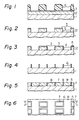
- a sapphire substrate 1 has a single crystalline silicon layer 2 epitaxially formed on it by a chemical vapor deposition (CVD) technique.
- a silicon nitride (Si 3 N 4 ) layer 3 is formed on the silicon layer 2 by a CVD technique and then a patterned photoresist layer 4 is formed on the Si 3 N 4 layer 3.
- the Si 3 N 4 layer 3 is selectively etched by a suitable etchant, e.g., a phosphoric acid (H 3 P0 4 ) solution, to form Si 3 N 4 islands 3 and to expose portions of the silicon layer 2.
- a suitable etchant e.g., a phosphoric acid (H 3 P0 4 ) solution
- the exposed portions of the silicon layer 2 are etched by a suitable etchant, e.g., carbon tetrafluoride (CF 4 ) gas, to form silicon islands 5.
- CF 4 carbon tetrafluoride
- the sapphire substrate 1 with the silicon islands 5 is then heated in an oxidizing atmosphere to thermally oxidize the sides. of the silicon islands 5, whereby silicon dioxide (Si0 2 ) layers 6 having a thickness of at least 30 nm are formed. Since the top surfaces of the silicon islands 5 are covered with the Si 3 N 4 islands 3, the top surfaces are not oxidized.
- the Si0 2 regions surround each of the silicon islands 5, as shown in Fig. 6.
- the Si 3 N 4 islands 3 are removed by etching by the H 3 P0 4 solution to expose the top surface of the silicon islands 5. Then the silicon islands 5 are removed by means of a plasma-etching technique using the CF 4 gas. The Si0 2 layers 6 remain on the sapphire substrate 1.
- silicon is epitaxially deposited on the sapphire substrate 1 by means of a CVD technique. Then, the deposited silicon layer is ground to the same level as the height of the Si0 2 layers 6. The result is single crystalline silicon islands (i.e., active regions) 7 surrounded by the Si0 2 layers 6 and a single crystalline silicon part 8, as illustrated in Figs. 5 and 6.
- Each of the silicon islands 7 is isolated from each other and from the silicon part 8 by the Si0 2 layer 6. Impurities are doped into the silicon islands 7 and gate electrodes with gate insulating layers are formed on the silicon islands 7 to form an element, such as an SOS type MOS FET (not shown).
- the width of the Si0 2 layers 6 i.e., isolation region between elements
- the width of the Si0 2 layers 6 can be considerably decreased, it is possible to increase the density of the semiconductor device.
- the distance between the adjacent silicon islands 7 is twice the width of the Si0 2 layers 6 plus the width of the unused silicon part 8. Therefore, the advantage of decreasing the Si0 2 layer width (i.e., the isolation region width) cannot be fully achieved.
- insulating layers having a relatively large area of conductor lines, including bonding pads cannot be formed without generating stray capacitance. Furthermore, it is very difficult to form a gate electrode with an end present between adjacent silicon (i.e., semiconductor) islands due to the shorter distance between islands compared with the alignment tolerance (e.g., about 1 pm) for patterning of about 1 um. If the gate electrode does not run across a semiconductor island (namely, the end of it is present above the semiconductor) a leakage current between the source region and the drain region occurs and the MOS FET obtained results in a defective product.
- the alignment tolerance e.g., about 1 pm
- Embodiments of the present invention provide a semiconductor device in which an insulator region isolating elements from one another is formed without resulting in unused semiconductor regions; a semiconductor device having a narrow insulator region having a width of as low as 30 nm; a method for producing a semiconductor device having both a narrow insulator region and wide insulating regions for conductor lines including bonding pads; a semiconductor device in which formation of the gate electrode is facilitated; and means of increasing the density of a semiconductor device.
- a semiconductor device comprises: a base body; an insulator region formed on the base body; first and second active regions of semiconductor islands adjacent to each other but respectively surrounded by said insulator region; and a gate electrode extending across said first active region, being a part of an FET formed in said first active region and ending at a portion of said second active region in which another FET is formed, i.e. with an end of the gate electrode lying above the adjacent semiconductor island.
- said insulator region comprises first and second stripe portions extending in different directions from each other and also. a portion formed at a cross point of the first and second stripe portions, said portion being wider than the first and second stripe portions. It is preferable that the width of the stripe insulator portions be from 30 nm to 2 pm. The narrower the width of the stripe insulator portion becomes, the denser the semiconductor device which can be produced.
- the stripe insulator portions are formed by oxidising sides of semiconductor islands formed on an insulating substrate.
- a sapphire substrate 21 has a single crystalline silicon layer 22 having a thickness of, e.g., about 0.6 um (micrometers) epitaxially formed by a CVD technique.
- a Si 3 N 4 layer 23 having a thickness of, e.g., from 0.2 to 0.3 pm is formed on the silicon layer 22 by a CVD technique.
- a patterned photoresist layer (not shown) is formed on the Si 3 N 4 layer 23.
- the Si 3 N 4 layer 23 and the silicon layer 22 are successively etched by means of a plasma-etching technique using CF 4 gas. Then, the patterned photoresist layer is removed to expose the patterned Si 3 N 4 layer 23 and silicon layer 22.
- the patterned Si 3 N 4 layer 23 comprises island portions 23A, 23B, and 23C and bridge portions 23D and 23E which connect adjacent island portions at corners thereof the island portions.
- next another photoresist layer (not shown) is applied on the entire surface of the patterned Si 3 N 4 layer 23 and the sapphire substrate 21, is exposed and is developed to form openings in the photoresist layer in which openings the bridge portions 23D and 23E are exposed.
- the bridge portions 23D and 24E of the Si 3 N 4 layer 23 are removed by a plasma-etching technique using CF 4 gas.
- portions of the silicon layer 22 located under the bridge portions 23D and 24E are successively etched by the plasma-etching technique so as to decrease the thickness of the silicon layer 22 by about half (i.e., about 0.3 ⁇ m).
- the Si 3 N 4 island portions 23A, 23B, and 23C and the patterned silicon layer 22 remain, as illustrated in Fig. 8.
- the island portions 23A, 23B, and 23C are separated from each other, and the patterned silicon layer 22 comprises island portions 22A, 22B, and 22C lying under the Si 3 N 4 island portions 23A, 23B, and 23C, respectively, and thin bridge portions 22D and 22E.
- the sapphire substrate 21 is then heated in an oxidizing atmosphere to thermally oxidize the exposed surface of the patterned silicon layer 22.
- the sides of the island portion 22A, 22B, and 22C are oxidized to form silicon dioxide (Si0 2 ) stripes 24A having a thickness of, e.g., 0.6 um.
- the bridge portions 22D and 22E are completely oxidized to form wide silicon dioxide (Si0 2 ) portions 24B.
- the Si 3 N 4 island portions 23A, 23B, and 23C and the silicon island portions 22A, 22B, and 23C are successively removed by means of a plasma-etching technique using CF 4 gas.
- the Si 3 N 4 island portions by means of a wet-etching technique using a H 3 P0 4 solution and then to remove the silicon island portions by means of a plasma-etching technique using trifluormethane gas or by means of wet-etching technique or by means of a wet-etching technique using a solution of hydrofluoric acid and nitric acid. Since the above-mentioned etchant etches little silicon dioxide, the SiO 2 stripes 24A and the wide SiO 2 portions 24B constituting an insulator region 24 remain, as illustrated in Fig. 9. In this case, the wide Si0 2 portions 24B have a height of about 0.6 um, almost the same as the thickness of the silicon layer 22 (namely, the same level as the SiO 2 stripes 24A), and connect the Si0 2 stripes.
- silicon is epitaxially grown on the sapphire substrate 21 by means of a CVD technique.
- the grown silicon layer is ground to the same level as the height of the Si0 2 stripes 24A (i.e., the height of the insulator region 24).
- single crystalline silicon islands (i.e., active regions) 25A through 25F isolated from each other by the insulator region 24 are formed.
- a gate insulating layer, a gate electrode, doped regions are formed.
- a Si0 2 layer for gate insulating layers 28A and 28B is deposited on the entire surface of the silicon islands 25A through 25F and the insulator region 24 by means of a CVD technique.
- a polycrystalline silicon layer for gate electrodes 29A and 29B (Fig. 11) is deposited on the Si0 2 layer by means of a CVD technique.
- a patterned photoresist layer (not shown) is formed on the polycrystalline silicon layer.
- the polycrystalline silicon layer and the Si0 2 layer are etched to form the polycrystalline silicon gates 29A and 29B and the gate insulating layers 28A and 28B, respectively, as illustrated in Fig. 11.
- another patterned photoresist layer is formed on the predetermined surface.
- impurities phosphorous, boron, etc.
- two SOS type MOS FET's are produced.
- the gate electrodes 29A and 29B run across the silicon islands 25B and 25E and the ends 30A and 30B are present above the adjacent silicon islands 25E and 25D, respectively.
- the difficult task of forming gate electrodes with ends above a Si0 2 stripe i.e., a narrow isolation region having a width of, e.g., about 0.6 um is unnecessary.
- the total area of the isolation region can be decreased as compared with a conventional semiconductor device. Therefore, the density of the semiconductor device can be increased. It is possible to form large Si0 2 layers for conductor lines and bonding pads on the sapphire substrate in the same manner as the formation of the wide Si0 2 portions of the insulator region.
- an insulator region 31 comprising very narrow (i.e., thin) Si0 2 strips 31A and wide and thin Si0 2 portions 31 B is formed, as illustrated in Fig. 12.
- the bridge portions 22D and 22E are etched to a very thin thickness of, e.g., about 15 nm.
- the sides of the island portions 22A, 22B, and 22C are oxidized to form Si0 2 stripes 31A having a height of 6.0 um and a width of 30 nm.
- the thin bridge portions 22D and 22E are completely oxidized to form the wide and thin Si0 2 portions 31 B having at thickness of 30 nm.
- the formation of silicon islands, the formation of gate electrodes with gate insulating layers, and the doping of impurities are then carried out in a similar manner to the above-mentioned manner to produce SOS type MOS FET's.
Landscapes
- Thin Film Transistor (AREA)
Claims (7)
Applications Claiming Priority (4)
| Application Number | Priority Date | Filing Date | Title |
|---|---|---|---|
| JP57049765A JPS58166761A (ja) | 1982-03-26 | 1982-03-26 | 半導体装置の製造方法 |
| JP49765/82 | 1982-03-26 | ||
| JP54594/82 | 1982-03-31 | ||
| JP57054594A JPS58171864A (ja) | 1982-03-31 | 1982-03-31 | 半導体装置 |
Publications (3)
| Publication Number | Publication Date |
|---|---|
| EP0090624A2 EP0090624A2 (fr) | 1983-10-05 |
| EP0090624A3 EP0090624A3 (en) | 1986-03-26 |
| EP0090624B1 true EP0090624B1 (fr) | 1989-07-26 |
Family
ID=26390217
Family Applications (1)
| Application Number | Title | Priority Date | Filing Date |
|---|---|---|---|
| EP83301696A Expired EP0090624B1 (fr) | 1982-03-26 | 1983-03-25 | Dispositif semi-conducteur du type MOS et son procédé de fabrication |
Country Status (3)
| Country | Link |
|---|---|
| US (1) | US4665419A (fr) |
| EP (1) | EP0090624B1 (fr) |
| DE (1) | DE3380285D1 (fr) |
Families Citing this family (10)
| Publication number | Priority date | Publication date | Assignee | Title |
|---|---|---|---|---|
| US5198377A (en) * | 1987-07-31 | 1993-03-30 | Kinya Kato | Method of manufacturing an active matrix cell |
| US4918504A (en) * | 1987-07-31 | 1990-04-17 | Nippon Telegraph And Telephone Corporation | Active matrix cell |
| US5719065A (en) | 1993-10-01 | 1998-02-17 | Semiconductor Energy Laboratory Co., Ltd. | Method for manufacturing semiconductor device with removable spacers |
| TW374196B (en) * | 1996-02-23 | 1999-11-11 | Semiconductor Energy Lab Co Ltd | Semiconductor thin film and method for manufacturing the same and semiconductor device and method for manufacturing the same |
| US6173352B1 (en) * | 1997-08-21 | 2001-01-09 | Ericsson Inc. | Mobile computer mounted apparatus for controlling enablement and indicating operational status of a wireless communication device associated with the mobile computer |
| US6686623B2 (en) | 1997-11-18 | 2004-02-03 | Semiconductor Energy Laboratory Co., Ltd. | Nonvolatile memory and electronic apparatus |
| JP2000012864A (ja) * | 1998-06-22 | 2000-01-14 | Semiconductor Energy Lab Co Ltd | 半導体装置の作製方法 |
| US6271101B1 (en) | 1998-07-29 | 2001-08-07 | Semiconductor Energy Laboratory Co., Ltd. | Process for production of SOI substrate and process for production of semiconductor device |
| JP4476390B2 (ja) | 1998-09-04 | 2010-06-09 | 株式会社半導体エネルギー研究所 | 半導体装置の作製方法 |
| US7134631B2 (en) * | 2004-06-10 | 2006-11-14 | Loth John L | Vorticity cancellation at trailing edge for induced drag elimination |
Family Cites Families (6)
| Publication number | Priority date | Publication date | Assignee | Title |
|---|---|---|---|---|
| US3484662A (en) * | 1965-01-15 | 1969-12-16 | North American Rockwell | Thin film transistor on an insulating substrate |
| GB1160744A (en) * | 1965-11-05 | 1969-08-06 | Plessey Co Ltd | Improvements in or relating to Semiconductor Devices |
| US3658586A (en) * | 1969-04-11 | 1972-04-25 | Rca Corp | Epitaxial silicon on hydrogen magnesium aluminate spinel single crystals |
| US3743552A (en) * | 1970-01-30 | 1973-07-03 | North American Rockwell | Process for coplanar semiconductor structure |
| DE2927824A1 (de) * | 1978-07-12 | 1980-01-31 | Vlsi Technology Res Ass | Halbleitervorrichtungen und ihre herstellung |
| US4418470A (en) * | 1981-10-21 | 1983-12-06 | General Electric Company | Method for fabricating silicon-on-sapphire monolithic microwave integrated circuits |
-
1983
- 1983-03-25 DE DE8383301696T patent/DE3380285D1/de not_active Expired
- 1983-03-25 EP EP83301696A patent/EP0090624B1/fr not_active Expired
-
1986
- 1986-04-01 US US06/846,486 patent/US4665419A/en not_active Expired - Lifetime
Also Published As
| Publication number | Publication date |
|---|---|
| EP0090624A3 (en) | 1986-03-26 |
| DE3380285D1 (en) | 1989-08-31 |
| EP0090624A2 (fr) | 1983-10-05 |
| US4665419A (en) | 1987-05-12 |
Similar Documents
| Publication | Publication Date | Title |
|---|---|---|
| KR100306935B1 (ko) | 집적회로내에트렌치절연구조물을형성하는방법 | |
| US6197661B1 (en) | Semiconductor device with trench isolation structure and fabrication method thereof | |
| KR100249632B1 (ko) | 반도체 장치 및 그 제조방법 | |
| US5834816A (en) | MOSFET having tapered gate electrode | |
| KR100223103B1 (ko) | 위치맞춤마크의 형성방법 | |
| EP0090624B1 (fr) | Dispositif semi-conducteur du type MOS et son procédé de fabrication | |
| JPS5836508B2 (ja) | 半導体装置の製造方法 | |
| US4885261A (en) | Method for isolating a semiconductor element | |
| EP0140749B1 (fr) | Procédé de fabrication d'un dispositif semi-conducteur complémentaire à isolement diélectrique | |
| US4722912A (en) | Method of forming a semiconductor structure | |
| KR100287181B1 (ko) | 트렌치소자분리영역을갖는반도체소자및그제조방법 | |
| JPH0656858B2 (ja) | 電荷結合素子の製造方法 | |
| JP3109549B2 (ja) | 半導体装置の製造方法 | |
| JPH0368170A (ja) | 薄膜半導体素子の製造方法 | |
| JP2775772B2 (ja) | 半導体装置の製造方法 | |
| JPH0547993B2 (fr) | ||
| JP3189320B2 (ja) | 半導体装置の製造方法 | |
| JPS61172346A (ja) | 半導体集積回路装置 | |
| JPH09205137A (ja) | 素子分離領域形成法 | |
| JP2671359B2 (ja) | 半導体装置の製造方法 | |
| JPH01144648A (ja) | 半導体装置 | |
| KR100257081B1 (ko) | 다결정 실리콘 산화공정을 이용한 반도체 소자 배선 제조방법 | |
| JPH0389532A (ja) | 半導体装置の製造方法 | |
| JPH0687481B2 (ja) | アイソレ−シヨンの製造方法 | |
| JPH03177072A (ja) | 半導体装置及びその製造方法 |
Legal Events
| Date | Code | Title | Description |
|---|---|---|---|
| PUAI | Public reference made under article 153(3) epc to a published international application that has entered the european phase |
Free format text: ORIGINAL CODE: 0009012 |
|
| AK | Designated contracting states |
Designated state(s): DE FR GB |
|
| PUAL | Search report despatched |
Free format text: ORIGINAL CODE: 0009013 |
|
| AK | Designated contracting states |
Kind code of ref document: A3 Designated state(s): DE FR GB |
|
| 17P | Request for examination filed |
Effective date: 19860812 |
|
| 17Q | First examination report despatched |
Effective date: 19880118 |
|
| GRAA | (expected) grant |
Free format text: ORIGINAL CODE: 0009210 |
|
| AK | Designated contracting states |
Kind code of ref document: B1 Designated state(s): DE FR GB |
|
| REF | Corresponds to: |
Ref document number: 3380285 Country of ref document: DE Date of ref document: 19890831 |
|
| ET | Fr: translation filed | ||
| PLBE | No opposition filed within time limit |
Free format text: ORIGINAL CODE: 0009261 |
|
| STAA | Information on the status of an ep patent application or granted ep patent |
Free format text: STATUS: NO OPPOSITION FILED WITHIN TIME LIMIT |
|
| 26N | No opposition filed | ||
| PGFP | Annual fee paid to national office [announced via postgrant information from national office to epo] |
Ref country code: FR Payment date: 19990309 Year of fee payment: 17 |
|
| PGFP | Annual fee paid to national office [announced via postgrant information from national office to epo] |
Ref country code: GB Payment date: 19990325 Year of fee payment: 17 |
|
| PGFP | Annual fee paid to national office [announced via postgrant information from national office to epo] |
Ref country code: DE Payment date: 19990406 Year of fee payment: 17 |
|
| PG25 | Lapsed in a contracting state [announced via postgrant information from national office to epo] |
Ref country code: GB Free format text: LAPSE BECAUSE OF NON-PAYMENT OF DUE FEES Effective date: 20000325 |
|
| GBPC | Gb: european patent ceased through non-payment of renewal fee |
Effective date: 20000325 |
|
| PG25 | Lapsed in a contracting state [announced via postgrant information from national office to epo] |
Ref country code: FR Free format text: LAPSE BECAUSE OF NON-PAYMENT OF DUE FEES Effective date: 20001130 |
|
| REG | Reference to a national code |
Ref country code: FR Ref legal event code: ST |
|
| PG25 | Lapsed in a contracting state [announced via postgrant information from national office to epo] |
Ref country code: DE Free format text: LAPSE BECAUSE OF NON-PAYMENT OF DUE FEES Effective date: 20010103 |