EP0091984A2 - Integrierte Schaltungsanordnungen mit dielektrischen Isolationsmassen und Verfahren zur Herstellung dieser Anordnungen - Google Patents
Integrierte Schaltungsanordnungen mit dielektrischen Isolationsmassen und Verfahren zur Herstellung dieser Anordnungen Download PDFInfo
- Publication number
- EP0091984A2 EP0091984A2 EP82108596A EP82108596A EP0091984A2 EP 0091984 A2 EP0091984 A2 EP 0091984A2 EP 82108596 A EP82108596 A EP 82108596A EP 82108596 A EP82108596 A EP 82108596A EP 0091984 A2 EP0091984 A2 EP 0091984A2
- Authority
- EP
- European Patent Office
- Prior art keywords
- semiconductor substrate
- groove
- conductivity type
- grooves
- impurity
- Prior art date
- Legal status (The legal status is an assumption and is not a legal conclusion. Google has not performed a legal analysis and makes no representation as to the accuracy of the status listed.)
- Granted
Links
Images


Classifications
-
- H—ELECTRICITY
- H10—SEMICONDUCTOR DEVICES; ELECTRIC SOLID-STATE DEVICES NOT OTHERWISE PROVIDED FOR
- H10D—INORGANIC ELECTRIC SEMICONDUCTOR DEVICES
- H10D62/00—Semiconductor bodies, or regions thereof, of devices having potential barriers
- H10D62/10—Shapes, relative sizes or dispositions of the regions of the semiconductor bodies; Shapes of the semiconductor bodies
- H10D62/102—Constructional design considerations for preventing surface leakage or controlling electric field concentration
- H10D62/112—Constructional design considerations for preventing surface leakage or controlling electric field concentration for preventing surface leakage due to surface inversion layers, e.g. by using channel stoppers
-
- H—ELECTRICITY
- H10—SEMICONDUCTOR DEVICES; ELECTRIC SOLID-STATE DEVICES NOT OTHERWISE PROVIDED FOR
- H10W—GENERIC PACKAGES, INTERCONNECTIONS, CONNECTORS OR OTHER CONSTRUCTIONAL DETAILS OF DEVICES COVERED BY CLASS H10
- H10W10/00—Isolation regions in semiconductor bodies between components of integrated devices
- H10W10/01—Manufacture or treatment
- H10W10/011—Manufacture or treatment of isolation regions comprising dielectric materials
- H10W10/014—Manufacture or treatment of isolation regions comprising dielectric materials using trench refilling with dielectric materials, e.g. shallow trench isolations
- H10W10/0143—Manufacture or treatment of isolation regions comprising dielectric materials using trench refilling with dielectric materials, e.g. shallow trench isolations comprising concurrently refilling multiple trenches having different shapes or dimensions
-
- H—ELECTRICITY
- H10—SEMICONDUCTOR DEVICES; ELECTRIC SOLID-STATE DEVICES NOT OTHERWISE PROVIDED FOR
- H10W—GENERIC PACKAGES, INTERCONNECTIONS, CONNECTORS OR OTHER CONSTRUCTIONAL DETAILS OF DEVICES COVERED BY CLASS H10
- H10W10/00—Isolation regions in semiconductor bodies between components of integrated devices
- H10W10/01—Manufacture or treatment
- H10W10/011—Manufacture or treatment of isolation regions comprising dielectric materials
- H10W10/014—Manufacture or treatment of isolation regions comprising dielectric materials using trench refilling with dielectric materials, e.g. shallow trench isolations
- H10W10/0145—Manufacture or treatment of isolation regions comprising dielectric materials using trench refilling with dielectric materials, e.g. shallow trench isolations of trenches having shapes other than rectangular or V-shape
-
- H—ELECTRICITY
- H10—SEMICONDUCTOR DEVICES; ELECTRIC SOLID-STATE DEVICES NOT OTHERWISE PROVIDED FOR
- H10W—GENERIC PACKAGES, INTERCONNECTIONS, CONNECTORS OR OTHER CONSTRUCTIONAL DETAILS OF DEVICES COVERED BY CLASS H10
- H10W10/00—Isolation regions in semiconductor bodies between components of integrated devices
- H10W10/01—Manufacture or treatment
- H10W10/011—Manufacture or treatment of isolation regions comprising dielectric materials
- H10W10/014—Manufacture or treatment of isolation regions comprising dielectric materials using trench refilling with dielectric materials, e.g. shallow trench isolations
- H10W10/0148—Manufacture or treatment of isolation regions comprising dielectric materials using trench refilling with dielectric materials, e.g. shallow trench isolations comprising introducing impurities in side walls or bottom walls of trenches, e.g. for forming channel stoppers
-
- H—ELECTRICITY
- H10—SEMICONDUCTOR DEVICES; ELECTRIC SOLID-STATE DEVICES NOT OTHERWISE PROVIDED FOR
- H10W—GENERIC PACKAGES, INTERCONNECTIONS, CONNECTORS OR OTHER CONSTRUCTIONAL DETAILS OF DEVICES COVERED BY CLASS H10
- H10W10/00—Isolation regions in semiconductor bodies between components of integrated devices
- H10W10/10—Isolation regions comprising dielectric materials
- H10W10/17—Isolation regions comprising dielectric materials formed using trench refilling with dielectric materials, e.g. shallow trench isolations
-
- H—ELECTRICITY
- H10—SEMICONDUCTOR DEVICES; ELECTRIC SOLID-STATE DEVICES NOT OTHERWISE PROVIDED FOR
- H10W—GENERIC PACKAGES, INTERCONNECTIONS, CONNECTORS OR OTHER CONSTRUCTIONAL DETAILS OF DEVICES COVERED BY CLASS H10
- H10W20/00—Interconnections in chips, wafers or substrates
- H10W20/01—Manufacture or treatment
- H10W20/021—Manufacture or treatment of interconnections within wafers or substrates
Definitions
- the present invention relates to a semiconductor device and a method for manufacturing the same and, more particularly, to an improvement in an element isolation technique of a metal oxide semiconductor large scale integrated circuit (MOSLSI) together with an improvement in a diffusion wiring layer and stabilization of a substrate potential.
- MOSLSI metal oxide semiconductor large scale integrated circuit
- Selective oxidation is generally adopted to isolate semiconductor elements from each other in the process for manufacturing a semiconductor device, especially, a MOSLSI.
- the selective oxidation will be described with reference to an n-channel MOSLSI.
- an SiO 2 film 2 is grown on a p-type silicon substrate 1 which has a crystal plane of (100).
- An Si 3 N 4 film 3 is then deposited on the SiO 2 film 2.
- a photoresist pattern 4 which corresponds to a prospective element formation region is formed by photoetching. Using the photoresist pattern 4 as a mask, part of the Si 3 N 4 film 3 which does not correspond to the prospective element formation region is etched to form an Si 3 N 4 pattern 3'. Thereafter, boron is ion-implanted to form a p +- type region 5 as a channel stopper in the field region (Fig. 1B).
- a thick field oxide film 6 is selectively grown by wet oxidation using the Si 3 N 4 pattern 3' (Fig. 1C) as a mask.
- the Si 3 N 4 pattern 3' and the SiO 2 film 2 are etched, and an element formation region 7 which is isolated by the field oxide film 6 is formed (Fig. 1D).
- a gate electrode 9 which comprises polycrystalline silicon is formed in the element formation region 7 through a gate oxide film 8.
- Arsenic is ion-implanted in the element formation region 7 and is thermally diffused to form n + -type regions 10 and 11 which are respectively defined as the source and drain.
- a CVD-SiO 2 film 12 which functions as an insulating interlayer is deposited.
- Contact holes 13 which correspond to the n +- type regions 10 and 11 and the gate electrode 9 are formed in the CVD-SiO 2 film 12.
- Aluminum wirings 14 are deposited in the contact holes 13 to prepare an n - channel MOSLSI (Fig. 1F) .
- Fig. 2 is a detailed sectional view showing a structure when the field oxide film 6 is formed using the Si 3 N 4 pattern 3' as a mask, shown in Fig. 1C.
- the field oxide film 6 grows to extend under the Si 3 N 4 pattern 3' (region F in Fig. 2). Since an oxidant is diffused through the thin SiO 2 film 2 under the Si 3 N 4 pattern 3' during field oxidation, the field oxide film 6 has a portion D which is a bird's beak and a portion E which is a thick portion along the transverse direction of the field oxide film 6.
- the length of region F is about 1 ⁇ m when the field oxide film 6 of 1 ⁇ m thickness is grown under the condition that the Si3N 4 pattern 3' and the SiO 2 film 2 have the thickness of 1,000 A.
- a width C of the field region cannot be less than 4 ⁇ m since the length of the region F is 1 ⁇ m when a distance A between the Si 3 N 4 patterns 3' is 2 ⁇ m.
- a highly integrated LSI cannot be obtained.
- a method has been recently proposed wherein the thickness of the Si 3 N 4 pattern 3' is increased and the thickness of the underlying SiO 2 film 2 is decreased to prevent the bird's beak ⁇ portion D).
- boron When boron is ion-implated to form a channel stopper, boron is transversely diffused during the field oxidation. Part of the element formation region 7 becomes the p +- type region 5 as shown in Fig. 3A due to redistribution of boron previously ion-implanted for the channel stopper in the transverse direction during field oxidation.
- the width of the effective element region is decreased from a width G to a width H. As a result, a current flowing through the transistor is decreased, and the threshold voltage is increased, resulting in the narrow channel effect. This effect is a significant problem when the semiconductor element is micronized.
- the p -type region 5 extends transversely, the p-n junction between the n +- type region 11 (10) and the p +- type region 5 is widened as shown in Fig. 3B.
- the stray capacitance between the substrate 1 and the n +- type regions 10 and 11 is increased. The stray capacitance cannot be neglected when the semiconductor element is micronized.
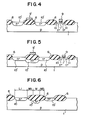
- n +- type wiring layer 10' and a polycrystalline silicon electrode 9' on the field oxide film 6 (Fig. 4).
- the n + -type layer 10" must be formed under the field oxide film 6.
- an impurity such as phosphorus or arsenic must be doped prior to field oxidation.
- the concentration of the impurity is generally high, the n-type doped impurity is out-diffused at the initial period of field oxidation, so that the p-type region on the surface of the substrate may often be changed to an n-type region.
- a substrate 1 is mounted on a bed 15 of the package.
- the potentials of element regions 16 1 to 16 3 for the source, drain and so on fluctuate in accordance with the operation state.
- a current flows through the substrate 1 in accordance with changes in the potentials of the element regions 16 1 to 163.
- the current flows through a path of the element region 16 1 , a resistor Rl, the bed 15, the element region 16 1 , a register R2, the bed 15, the element region 16 1 , a register R5, the bed 15 and so on when the bed 15 is electrically conductive and the substrate 1 is electrically connected to the bed 15.
- a potential of the substrate 1 in the vicinity of the element region 16 1 fluctuates in correspondence with a voltage drop due to the current flow described above.
- a variation in the potential is undesirable for circuit operation.
- the voltage of the element region 16 1 is changed and when the potential of the element region 16 2 is not changed, the potential of the substrate 1 in the vicinity of the part between the element regions 16 1 and 16 2 is changed.
- electrical characteristics of the element vary in accordance with points on the pellet, which is inconvenient.
- the internal resistance of the substrate must be decreased.
- the resistance of resistors R5 to R8 and resistors' B to Rll is determined by the impurity concentration of the substrate and the film thickness of the substrate which is connected to the bed.
- the resistance of the resistors R5 to R8 and R9 to Rll is about hundred ohms to several hundreds of ohms. Therefore, the internal resistance can hardly be decreased.
- the resistance of the resistors Rl to R4 can be decreased regardless of the electrical characteristics of the element since these resistors provide the internal resistance of the field region 6.
- the concentration of the p-type impurity cannot be increased, so the resistance is very high.
- the impurity is ion-implanted in the field region at a dose of 1 x 10 cm , and the sheet resistance of the p +- type layer is about 10 kilohms/ ⁇ .
- the present invention has been made to eliminate the above problems and has for its object to provide a semiconductor device and a method for manufacturing the same, wherein a high packing density and a high performance are accomplished by a novel element isolation technique.
- a mask such as a photoresist pattern is formed in a region of a semiconductor substrate except for the groove formation region and the exposed portion of the substrate is selectively etched by reactive ion etching to a desired depth to form a groove, using the photoresist pattern as a mask.
- the wall of the groove can be formed substantially vertical if reactive ion is adopted.
- any other etching means may be used to form an inverted tapered groove. At least one groove may be formed. Further, the depth of the groove may be changed from one groove to another.
- An impurity whose conductivity type is opposite to that of the substrate (if a p-type substrate is used, phosphorus or arsenic is used as the impurity; if an n-type substrate is used, boron is used as the impurity) is ion-implanted at a dose of 1 x 10 16 cm -2 in the groove using the photoresist pattern as the mask. Alternatively, the impurity is diffused. Prior to the doping of the impurity, a photoresist pattern may be formed to cover part of the groove or some grooves, and doping may be performed.
- boron whose conductivity type is the same as the substrate may be doped in part or over all the groove to form a channel stopper.
- the impurity may be obliquely or transversely,,diffused to form an impurity region in the side surfaces of the groove.
- the depth of the groove is made greater than a diffusion depth xj of the diffusing region for forming the source and drain in the subsequent process.
- the depth of the groove must be smaller than the depth xj when it is desired to isolate the n +- type buried region and the n +- type source and drain regions or to electrically contact the n +- type buried region with the n +- type source and drain regions.
- an insulating film is deposited to cover the entire surface of the semiconductor substrate, including the area of the groove, to a thickness at least greater than half the width of the shorter side of the opening of the groove.
- the insulating film is deposited to fill at least one groove.
- the insulating film may comprise Si0 2 , Si 3 N 4 or Al 2 O 3 .
- a low-melting point insulating material such as phosphorus silicate glass (PSG), boron silicate glass (BSG), and the like may be used for the insulating film.
- the insulating material described above may be deposited by the CVD method, the PVD method, such as the sputtering method, or the like.
- a recess which communicates with the opening of the insulating material filled in the groove is formed.
- the insulating material in the groove is etched through the recess, which is inconvenient.
- the entire surface of the semiconductor substrate has grooves prior to deposition of the insulating material, and at least part of the groove may be oxidized or nitrified to form an oxide or nitride film so as not to block the groove.
- Doping of the impurity may be performed before or after the oxide or nitride film is formed.
- the resultant field region comprises the insulating film and the dense oxide or nitride film which contacts the grooved part of the substrate.
- the element isolation performance is greatly improved.
- a low-melting point material such as boron, phosphorus, or arsenic is doped on part or all of the surface layer of the insulating film. Thereafter, the insulating film is annealed to melt the doping layer.
- a low-melting point insulating material such as BSG, PSG and arsenic silicate glass (AsSG) may be deposited on part or all of the insulating film and may be melted.
- a low-melting point insulating material such as BSG, PSG and arsenic silicate glass (AsSG) may be deposited on part or all of the insulating film and may be melted.
- the insulating film deposited on the semiconductor substrate is etched without using the mask until the surface of the semiconductor substrate, except for the inner wall and bottom of the groove, is exposed. Thus, the insulating material is left in the groove to form a field region. In this case, entire surface etching using a liquid etchant or a plasma etchant, or reactive ion etching can be adopted. Thereafter, active elements such as a MOS element or bipolar semiconductor element are formed in the element formation region which is isolated by the field region to prepare a semiconductor device.
- a groove is formed in the semiconductor substrate, and an impurity whose conductivity type is opposite to that of the substrate is ion-implanted or is diffused.
- an insulating material is deposited to cover the entire surface of the substrate, including the groove, to a thickness greater than half the width of the shorter side of at least one groove.
- the insulating film is then etched to expose the surface of the substrate and to leave the insulating material in the groove. Without providing a margin for mask alignment, the buried diffusion layer can be formed in the groove in a self-aligned manner. Further, the insulating material can be left on the buried diffusion layer, so that the field region can be readily formed. Therefore, the following effects are obtained:
- an insulating material is deposited to cover the entire surface of the semiconductor substrate to a thickness greater than half of the shorter width of an opening of at least one groove.
- a mask such as a photoresist pattern is formed on one or both of a first portion of the insulating film which includes at least part of the groove filled with the insulating material to its opening, and a second portion of the insulating film which excludes the groove and is defined as the prospective field region.
- the exposed portion of the insulating film is etched to expose the surface of the substrate and to leave the insulating material in the groove, using the photoresist film as the mask.
- the field region is formed in the groove and on the substrate.
- the field region formed on the substrate includes a field region integrally formed with the field region in the groove.
- active elements such as a MOS element or bipolar semiconductor element are formed in the element formation region isolated by the field region to prepare a semiconductor device.
- a semiconductor device has a field region which comprises the field region embedded in the semiconductor substrate and the field region which is formed on the semiconductor substrate part excluding the grooved part and which is integral with the field region embedded in the substrate or is separated therefrom.
- first grooves are formed which include at least two adjacent grooves.
- the first grooves may include at least one groove which is apart from the set of grooves.
- the insulating material may comprise Si0 2 , si 3 N 4 or Al 2 O 3 .
- a low-melting point insulating material such as PSG, AsSG or BSG may be used as the insulating material.
- the insulating material is deposited by the CVD method or the PVD method, such as sputtering.
- an impurity whose conductivity type is the same as the substrate may be doped in parts of the first grooves to form a channel stopper region in the substrate.
- the surface layer of the semiconductor substrate which has the first grooves, or part of the surfaces of the grooves may be oxidized or nitrified so as not to block the grooves.
- a low-melting point insulating material may be formed thereon.
- the insulating film deposited on the semiconductor substrate is etched by exclusive etching using a liquid etchant or plasma etchant, or reactive ion etching without using a mask to expose the surface of the semiconductor substrate except for the first grooves, so that the insulating material is left in the set of at least two adjacent grooves to the level of their openings.
- the exposed part of the semiconductor substrate which is located between the set of at least two adjacent grooves filled with the insulating material is selectively etched to form a second groove between the first grooves.
- the insulating material is filled in the first grooves and is not substantially etched, while the semiconductor substrate is etched. Therefore, the second groove can be formed in a self-aligned manner even if part of the first grooves which include at least two adjacent grooves is exposed.
- an insulating material is deposited to cover the entire surface of the substrate to a thickness less than half the width of the shorter side of the opening of the second groove. The insulating materials described above can also be applied to this case.
- the insulating film is etched to expose the surface of the semiconductor substrate and to leave the insulating material in the second groove.
- the insulating material left in the first grooves which are located at two sides of the second groove is formed integrally with the insulating material left in the second groove.
- active elements such as a MOS element or a bipolar semiconductor element are formed in the element formation region isolated by the field region to prepare a semiconductor device.
- a field region which has a wide width without having a step can be obtained to provide a highly integrated, highly reliable, and high-performance semiconductor device.
- a mask such as a photoresist pattern is formed on the semiconductor substrate except for the prospective groove formation region. Thereafter, the exposed portion of the substrate is selectively etched by the same etching means as described above to a desired depth to form first grooves.
- An impurity whose conductivity type is opposite to that of the substrate is doped in at least part of the first grooves. Subsequently, the mask is removed, and the insulating material is deposited to cover the entire surface including the first grooves in the same manner as described above.
- the insulating film is etched without using the mask to expose the surface of the substrate and to leave the insulating material in the first grooves. Thereafter, an antioxidant film is selectively formed on the surface of the semiconductor substrate directly or through the insulating film.
- the antioxidant film may comprise a Si 3N4 film or Al 2 O 3 film.
- the part between the first grooves is selectively etched using the antioxidant film as a mask so that a second groove is formed between the first grooves.
- Field oxidation is then performed using the antioxidant film to fill the second groove with an oxide (insulating) film.
- the insulating film left in the first grooves is formed integrally with that of the second groove to prepare a wide field region.
- the first to fourth features are all concerned with the formation of wiring layers for isolating semiconductor elements by diffusing (or ion-implanting) an impurity whose conductivity type is opposite to that of the substrate.
- an impurity whose conductivity type is the same as that of the substrate is diffused (or ion-implated) in the groove to stabilize the substrate potential.
- the process for ion-implanting or diffusing the impurity into the groove is the same as that in the first feature except that an impurity whose conductivity type is the same as that of the substrate (boron is ion-implanted or diffused in a p-type substrate; phosphorus is ion-implanted or diffused in an n-type substrate) at a dose of 1 x 10 14 cm -2 or more.
- the groove is formed in the semiconductor substrate.
- the impurity whose conductivity type is the same as that of the substrate is doped at a predetermined dose.
- An insulating material is then deposited to cover the entire surface of the substrate including the groove to a thickness greater than half the width of the shorter side of an opening of at least one groove.
- the insulating film is then etched to expose the substrate and to leave the insulating material in the groove.
- a buried diffusion layer is formed with respect to the groove in a self-aligned manner without a mask alignment margin.
- the insulating material can be formed on the buried diffusion layer to form the field region. Therefore, in addition to effects (1), (2) and (5) of the first feature, the various effects are provided to be described below:
- the sixth feature is the same as the second feature except that an impurity whose conductivity type is the same as that of the substrate is ion-implanted (boron is used for a p-type substrate; phosphorus or arsenic is used for an n-type substrate) at a dose of 1 x 10 14 cm -2 or more, or is diffused in the ion-implantation or diffusion of the impurity in the groove.
- an impurity whose conductivity type is the same as that of the substrate is ion-implanted (boron is used for a p-type substrate; phosphorus or arsenic is used for an n-type substrate) at a dose of 1 x 10 14 cm -2 or more, or is diffused in the ion-implantation or diffusion of the impurity in the groove.
- a semiconductor device in addition to the various effects of the fifth feature, a further effect is obtained wherein a semiconductor device has the field region embedded in the semiconductor substrate and the field region which is formed on the semiconductor substrate except for the groove, and which is integral with the embedded field region or is separated therefrom.
- the seventh feature is the same as the third feature except that an impurity whose conductivity type is the same as that of the substrate is-ion-implanted or doped at a dose of 1 x 10 14 cm -2 in the ion-implantation or diffusion of the impurity in the groove.
- the seventh feature of the present invention in addition to the effects of the fifth feature, a further effect is obtained wherein the wide field region without any step can be formed to provide a highly integrated, highly reliable and high-performance semiconductor device.
- the eighth feature is the same as the fourth feature except that an impurity whose conductivity type is the same as that of the substrate is ion-implanted or doped at a dose of 1 x 10 14 cm -2 or more in the ion-implantation or diffusion step of the impurity in the groove.
- a semiconductor device can be obtained wherein the sheet resistance ps of the impurity region is 50 ohms/ ⁇ or less and its conductivity type is the same as that of the substrate. It is noted that the internal resistance is limited to eliminate adverse effects of a great potential difference between the semiconductor elements formed on the substrate when the semiconductor device is operated since the substrate resistance under the field region cannot be sufficiently decreased when the LSI pellet is mounted on the bed of the package.
- the width of the field region can be as small as 1 ⁇ m.
- the field region can be micronized in the LSI which can be highly integrated.
- margins Ml and M2 between the n +- type buried layer and the n +- type layer formed in the surface layer of the substrate become short.
- a leakage current tends to flow between the n + -type layers.
- the depth of the field region,106 is as great as 2 ⁇ m even though its width is short as shown in Fig. 10, so that a current does not leak between the n +- type layers.
- the surface of the substrate 101 between the field region and the element formation region is flat, as shown in Fig. 8E, so that excellent step coverage is provided when the aluminum electrodes 113 and 114 are deposited.
- the grooves 103 need not be filled with the n +- type layers. As shown in Fig. 12, the n +- type layers may be formed as needed, while the p +- type layers may be formed in the remaining grooves. Alternatively, the concentration of the impurity in the grooves need not be changed. Further, as shown in Fig. 13, the n +- type layer is partially formed in the groove 103.
- the photoresist pattern 102 is formed directly on the silicon substrate 101, and then grooves 103 are formed in the substrate 101 using the photoresist pattern 102 as a mask.
- the photoresist pattern 102 may be formed thereon, and the insulating film 115 and the substrate 101 may be selectively etched by reactive ion etching using the photoresist pattern 102 as a mask.
- contact holes 116 can be formed (Fig. 14B).
- the insulating film 115 formed on the silicon substrate 101 may be patterned, and then the silicon substrate 101 may be etched by reactive ion etching using the insulating pattern to form the grooves 103 (Fig. 15B).
- a p +- type region 104a as the channel stopper may be formed in the substrate portion under the field region 106"'.
- the MOSLSI obtained in the above example has the narrow field region 209' and the wide field region 209. Further, since the field regions 209 and 209' are formed, the level of the element formation region of the silicon substrate 201 is the same as that of the field regions. Therefore, when the Al electrodes 216 and 217 are formed, excellent step coverage is provided between the field regions and the element formation region. Further, since the n -type regions 204 and 204" as the buried diffusion regions are in the bottoms of the first grooves 203 1 to 203 5 and the second grooves 207 1 to 207 3 , the impurity is not diffused to the element formation region, thus providing a highly integrated LSI. In order to contact the buried diffusion layer and the surface diffusion layer, the same process as in Example 1 may be performed.
- the n +- type regions are formed under the CVD-Si0 2 film portions 205' and the CVD-SiO 2 film portions 208' in the above example, the n +- type regions may be formed under either the CVD-SiO 2 film portions 205' or 208' (Figs. 23A and 23B). Alternatively, small parts of the regions under the CVD-SiO 2 film portions 205' or 208' may be formed as the n -type regions. Further, parts of the regions under the CVD-Si0 2 film portions 205' and 208' may be formed to be p +- type regions.
- the n +- type region and the p + - type region may be mixed utilizing photoetching under the CVD-SiO 2 film portions 205' and/or 208'.
- the clearance for the channel stopper effect is secured.
- all or part of the surface of the semiconductor substrate, or at least part of the grooves may be oxidized or nitrided to form an oxide or nitride film without blocking the grooves.
- an impurity may be doped before or after the formation of the oxide or nitride film.
- a low-melting point material may be doped on all or part of the surface layer of the insulating film. Thereafter, the doped layer of the insulating film may be melted.
- a low-melting point insulating film may be deposited on all or part of the insulating film. Thereafter, the deposited insulating film may be melted.
- the buried diffusion layer is formed under the field film which has the same level as the silicon substrate and which has the desired width. Therefore, a highly integrated and high-performance LSI can be manufactured.
- an n +- type layer 304' may be formed under the field oxide film 311, and the n -type layers 304 are formed in the bottoms of the buried field insulating films 305 1 to 305 3 .
- p +- type layers 304a may be formed in the bottoms of the buried field insulating films 305 1 to 305 3 ; only part of the field regions need comprise an n +- type layer.
- Example 8 was substantially the same as Example 1 except that in step (i) boron instead of phosphorus was ion-implanted in grooves 103 at a dose of 1 x 10 16 cm -2 and at an acceleration voltage of 50 KeV, and annealing was then performed to diffuse the impurity so as to form p +- type regions 104' as the channel stoppers in the bottoms of the grooves 103. Thus, an n-channel MOSLSI was prepared, as shown in Fig. 28.
- the reference numerals used with reference to Example 1 denote the same parts in Fig. 28 unless otherwise indicated.
- the impurity concentration in the p +- type region 104' can be increased, so that its sheet resistance is as low as 10 to 20 ohms/D. Therefore, the variations in the substrate potentials with respect time and space can be improved. Other effects are the same as those obtained in Example 1.
- Example 9 was substantially the same as Example 2 except that boron was ion-implanted at a dose of 1 . x 10 16 cm -2 .
- the semiconductor device shown in Fig. 29 was prepared.
- the semiconductor device was substantially the same as that in Fig. 16C except that p +- type regions 104' were respectively formed in the bottoms of grooves 103 and 103'.
- Example 10 was substantially the same as Example 4 except that boron was ion-implanted at a dose of 1 x 10 16 cm -2 .
- a semiconductor device shown in Fig. 30 was prepared.
- the semiconductor device was substantially the same as that in Fig. 18D except that p +- type regions 104' were formed in the bottoms of grooves 1031 to 103 4 .
- p +- type regions may be formed under field regions 106 1 and 106 2 to be formed in the subsequent process (Fig. 31).
- Part of the p + -type region may be formed as an n +- type region if necessary.
- the n +- type region may be used as a wiring layer.
- Example 11 was substantially the same as Example 5 except that boron was ion-implanted at a dose of 1 x 10 16 cm -2 .
- a semiconductor device shown in Fig. 32 was prepared.
- the semiconductor device was substantially the same as that in Fig. 20E except that p +- type regions 104' were formed in the bottoms of grooves 103 1 to 103 3 .
- an n +- type region 104a' may be formed as a diffusion wiring layer in the substrate portion under the field region 106"'.
- Example 12 was substantially the same as Example 6 except that boron was ion-implanted at a dose of 1 x 10 16 cm -2 and at an acceleration voltage of 50 KeV.
- a semiconductor device was prepared wherein p +- type regions 204' were formed as channel stoppers in the bottoms of narrow and wide field regions, as shown in Fig. 34.
- regions below CVD-SiO 2 film portions 205' or 208' or both comprise p + -type regions.
- Only parts of the regions below the CVD-Si0 2 film portions 205' and 208' film portions may comprise a P + -type region. Further, the regions below either the CVD-SiO 2 film portions 205' or 208' may comprise p +- type regions. Further, p + - type regions and n + - type regions (wiring layers) may be mixed utilizing photoetching independently of the CVD-Si0 2 film portions 205' and 208'. Especially, as shown in Fig. 36, when p + -type regions 204' are respectively formed in the bottoms of two ends of the field region 209 and an n +- type region 204a' is formed at the center thereof, an excellent channel stopper effect is provided.
- Example 13 was substantially the same as Example 7 except that in step (iii) of Example 7 boron was ion-implanted in the grooves 303 at a dose of 1 x 10 16 cm -2 and at an acceleration voltage of 50 KeV to form p +- type regions 304', and that in step (viii) of Example 7 arsenic or phosphorus instead of boron was ion-implanted in the bottom of the groove 309 at a dose of 1 x 10 16 cm -2 and at an acceleration voltage of 50 KeV to form an n +- type region 310'.
- the semiconductor device shown in Fig. 37 was prepared. Other arrangements of the semiconductor device are the same as those in Fig. 25K.
- n +- type layers and the p +- type layers may be arbitrarily changed in the same manner described with reference to Figs. 26 and 27.
- the photoresist film 302 is used as a mask in the example shown in Figs. 25A to 25K.
- an insulating film 320 e.g., Si0 2 film
- the insulating film 320 and the silicon substrate 301 may be selectively etched to form a groove 303' (Fig. 38).
- the exposed portion of the silicon substrate may be etched using the pattern of the insulating film 320 as a mask to form the groove 303 (Fig. 39B).
- an insulating film 322 may be preformed in the groove 303 (Fig. 40).
- the insulating film 322 may be formed by oxidizing the silicon substrate 301.
- a CVD-SiO 2 film may be deposited in the groove 303.
- the width of the opening of the groove 303 is half the thickness of the insulating film 322.
- the buried field insulating films 305 1 to 305 3 may be recessed from the surface of the silicon substrate 301.
- the depths of the buried field insulating films 305 1 to 305 3 may vary.
- the antioxidant film 307 is deposited and patterned, the antioxidant film 307 and the silicon substrate 301 are etched. However, after the silicon substrate 301 is selectively etched to form the groove 309, the antioxidant film 307 may then be deposited and be selectively etched from the groove 309. Thereafter, field oxidation may be performed.
- the antioxidant film 307 is etched and the silicon substrate 301 is etched to form the groove 309
- field oxidation is performed.
- the silicon substrate 310 may be etched without performing field oxidation (Figs. 41A and 41B).
- the insulating 'film 306 need not be deposited.
- the thin insulating film 306 need not be etched and field oxidation can be performed unlike the case shown in Fig. 41A where the substrate (e.g., silicon substrate 301) is not oxidized in the field oxidation process.
- the field oxide film 311 may be etched using the antioxidant film 307 after the step shown in Fig. 41B is performed, so that a flat structure may be obtained (Fig. 42).
- the above step may be applied to a case where the silicon substrate 301 is etched and then field oxidation is performed. This is very effective in a case where alignment between the field oxide film 311 and the silicon substrate 301 is not accomplished since the thick filed oxide film 3ll is formed even if the silicon substrate 301 is etched.
- an impurity whose conductivity type is opposite to that of the substrate is ion-implanted substantially perpendicularly to the surface of the silicon substrate 301.
- the impurity may be obliquely ion-implanted with respect to the silicon substrate 301 to form n +- type regions 304" on the inner surfaces of the groove 303.
- the n +- type regions 304" may be formed by diffusion.
- the above ion-implantation may be applied to an impurity whose conductivity type is the same as that of the silicon substrate.
- the grooves have vertical or substantially vertical walls.
- the present invention is not limited to this.
- a wedge-shaped groove 403 whose surface is inclined by. an angle 6 with respect to the surface of the silicon substrate may be formed as shown in Figs. 44A and 44B.
- the thickness of an insulating film 405 is greater than (a x cot(6/2))/2 where reference symbol a denotes the width of the opening of the groove.
- a groove having tapered walls and a flat bottom may also be used.
- an insulating film 502 formed on a substrate 501 need not be etched to expose the surface of the substrate 501.
- An insulating film 502' may be left on the surface of the substrate 501 as shown in Fig. 45B.
- the insulating film 502' may be used as a gate film or an insulating interlayer, or a part thereof.
- grooves 503 are formed in the substrate 501 using a mask 504, and an insulating film 502 is then deposited on the mask 504.
- the insulating film 502 may be etched to leave the mask 504 on the substrate 501 (Fig. 46B).
Landscapes
- Element Separation (AREA)
Applications Claiming Priority (4)
| Application Number | Priority Date | Filing Date | Title |
|---|---|---|---|
| JP56146547A JPS5848437A (ja) | 1981-09-17 | 1981-09-17 | 半導体装置の製造方法 |
| JP146547/81 | 1981-09-17 | ||
| JP56161312A JPS5861642A (ja) | 1981-10-09 | 1981-10-09 | 半導体装置及びその製造方法 |
| JP161312/81 | 1981-10-09 |
Publications (3)
| Publication Number | Publication Date |
|---|---|
| EP0091984A2 true EP0091984A2 (de) | 1983-10-26 |
| EP0091984A3 EP0091984A3 (en) | 1986-08-20 |
| EP0091984B1 EP0091984B1 (de) | 1990-01-31 |
Family
ID=26477357
Family Applications (1)
| Application Number | Title | Priority Date | Filing Date |
|---|---|---|---|
| EP82108596A Expired EP0091984B1 (de) | 1981-09-17 | 1982-09-17 | Integrierte Schaltungsanordnungen mit dielektrischen Isolationsmassen und Verfahren zur Herstellung dieser Anordnungen |
Country Status (3)
| Country | Link |
|---|---|
| US (1) | US4491486A (de) |
| EP (1) | EP0091984B1 (de) |
| DE (1) | DE3280101D1 (de) |
Cited By (2)
| Publication number | Priority date | Publication date | Assignee | Title |
|---|---|---|---|---|
| WO1987003139A3 (en) * | 1985-11-15 | 1987-08-27 | Ncr Co | Process for trench oxide isolation of integrated devices |
| US6377723B1 (en) | 1999-01-13 | 2002-04-23 | The Furukawa Electric Co., Ltd | Optical waveguide circuit, and method for compensating the light transmission wavelength |
Families Citing this family (21)
| Publication number | Priority date | Publication date | Assignee | Title |
|---|---|---|---|---|
| JP3157357B2 (ja) * | 1993-06-14 | 2001-04-16 | 株式会社東芝 | 半導体装置 |
| US5575878A (en) * | 1994-11-30 | 1996-11-19 | Honeywell Inc. | Method for making surface relief profilers |
| KR100236097B1 (ko) * | 1996-10-30 | 1999-12-15 | 김영환 | 반도체 장치의 격리막 형성방법 |
| US6200880B1 (en) * | 1998-11-16 | 2001-03-13 | United Microelectronics Corp. | Method for forming shallow trench isolation |
| US7023069B2 (en) * | 2003-12-19 | 2006-04-04 | Third Dimension (3D) Semiconductor, Inc. | Method for forming thick dielectric regions using etched trenches |
| TWI401749B (zh) * | 2004-12-27 | 2013-07-11 | 3D半導體股份有限公司 | 用於高電壓超接面終止之方法 |
| US7439583B2 (en) * | 2004-12-27 | 2008-10-21 | Third Dimension (3D) Semiconductor, Inc. | Tungsten plug drain extension |
| CN101189710B (zh) * | 2005-04-22 | 2011-05-04 | 艾斯莫斯技术公司 | 具有氧化物衬里沟槽的超结器件和制造具有氧化物衬里沟槽的超结器件的方法 |
| US7446018B2 (en) * | 2005-08-22 | 2008-11-04 | Icemos Technology Corporation | Bonded-wafer superjunction semiconductor device |
| US7429772B2 (en) | 2006-04-27 | 2008-09-30 | Icemos Technology Corporation | Technique for stable processing of thin/fragile substrates |
| US7723172B2 (en) * | 2007-04-23 | 2010-05-25 | Icemos Technology Ltd. | Methods for manufacturing a trench type semiconductor device having a thermally sensitive refill material |
| US8580651B2 (en) * | 2007-04-23 | 2013-11-12 | Icemos Technology Ltd. | Methods for manufacturing a trench type semiconductor device having a thermally sensitive refill material |
| US20080272429A1 (en) * | 2007-05-04 | 2008-11-06 | Icemos Technology Corporation | Superjunction devices having narrow surface layout of terminal structures and methods of manufacturing the devices |
| DE102007035251B3 (de) | 2007-07-27 | 2008-08-28 | X-Fab Semiconductor Foundries Ag | Verfahren zur Herstellung von Isolationsgräben mit unterschiedlichen Seitenwanddotierungen |
| US20090085148A1 (en) * | 2007-09-28 | 2009-04-02 | Icemos Technology Corporation | Multi-directional trenching of a plurality of dies in manufacturing superjunction devices |
| CN101510557B (zh) * | 2008-01-11 | 2013-08-14 | 艾斯莫斯技术有限公司 | 具有电介质终止的超结半导体器件及制造该器件的方法 |
| US7795045B2 (en) * | 2008-02-13 | 2010-09-14 | Icemos Technology Ltd. | Trench depth monitor for semiconductor manufacturing |
| US7846821B2 (en) * | 2008-02-13 | 2010-12-07 | Icemos Technology Ltd. | Multi-angle rotation for ion implantation of trenches in superjunction devices |
| US8030133B2 (en) * | 2008-03-28 | 2011-10-04 | Icemos Technology Ltd. | Method of fabricating a bonded wafer substrate for use in MEMS structures |
| US8946814B2 (en) | 2012-04-05 | 2015-02-03 | Icemos Technology Ltd. | Superjunction devices having narrow surface layout of terminal structures, buried contact regions and trench gates |
| US9576842B2 (en) | 2012-12-10 | 2017-02-21 | Icemos Technology, Ltd. | Grass removal in patterned cavity etching |
Family Cites Families (20)
| Publication number | Priority date | Publication date | Assignee | Title |
|---|---|---|---|---|
| US3972751A (en) * | 1973-07-17 | 1976-08-03 | Owego Heat Treat, Inc. | Method of heat treating ferrous workpieces |
| US3966577A (en) * | 1973-08-27 | 1976-06-29 | Trw Inc. | Dielectrically isolated semiconductor devices |
| JPS5131186A (de) * | 1974-09-11 | 1976-03-17 | Hitachi Ltd | |
| JPS5347253B2 (de) * | 1974-10-16 | 1978-12-20 | ||
| US4032373A (en) * | 1975-10-01 | 1977-06-28 | Ncr Corporation | Method of manufacturing dielectrically isolated semiconductive device |
| NL178487C (nl) * | 1976-03-26 | 1986-04-01 | Stamicarbon | Inrichting en werkwijze voor het versproeien van een vloeistof. |
| US4044452A (en) * | 1976-10-06 | 1977-08-30 | International Business Machines Corporation | Process for making field effect and bipolar transistors on the same semiconductor chip |
| US4104086A (en) * | 1977-08-15 | 1978-08-01 | International Business Machines Corporation | Method for forming isolated regions of silicon utilizing reactive ion etching |
| US4139442A (en) * | 1977-09-13 | 1979-02-13 | International Business Machines Corporation | Reactive ion etching method for producing deep dielectric isolation in silicon |
| US4140558A (en) * | 1978-03-02 | 1979-02-20 | Bell Telephone Laboratories, Incorporated | Isolation of integrated circuits utilizing selective etching and diffusion |
| US4209380A (en) * | 1978-07-27 | 1980-06-24 | Ppg Industries, Inc. | Cathode element for electrolytic cell |
| DE2949360A1 (de) * | 1978-12-08 | 1980-06-26 | Hitachi Ltd | Verfahren zur herstellung einer oxidierten isolation fuer integrierte schaltungen |
| US4238278A (en) * | 1979-06-14 | 1980-12-09 | International Business Machines Corporation | Polycrystalline silicon oxidation method for making shallow and deep isolation trenches |
| US4211582A (en) * | 1979-06-28 | 1980-07-08 | International Business Machines Corporation | Process for making large area isolation trenches utilizing a two-step selective etching technique |
| JPS5636143A (en) * | 1979-08-31 | 1981-04-09 | Hitachi Ltd | Manufacture of semiconductor device |
| US4338138A (en) * | 1980-03-03 | 1982-07-06 | International Business Machines Corporation | Process for fabricating a bipolar transistor |
| US4318751A (en) * | 1980-03-13 | 1982-03-09 | International Business Machines Corporation | Self-aligned process for providing an improved high performance bipolar transistor |
| US4378630A (en) * | 1980-05-05 | 1983-04-05 | International Business Machines Corporation | Process for fabricating a high performance PNP and NPN structure |
| US4390393A (en) * | 1981-11-12 | 1983-06-28 | General Electric Company | Method of forming an isolation trench in a semiconductor substrate |
| JPS58165341A (ja) * | 1982-03-26 | 1983-09-30 | Toshiba Corp | 半導体装置の製造方法 |
-
1982
- 1982-09-16 US US06/418,802 patent/US4491486A/en not_active Expired - Lifetime
- 1982-09-17 EP EP82108596A patent/EP0091984B1/de not_active Expired
- 1982-09-17 DE DE8282108596T patent/DE3280101D1/de not_active Expired - Lifetime
Cited By (3)
| Publication number | Priority date | Publication date | Assignee | Title |
|---|---|---|---|---|
| WO1987003139A3 (en) * | 1985-11-15 | 1987-08-27 | Ncr Co | Process for trench oxide isolation of integrated devices |
| US4753901A (en) * | 1985-11-15 | 1988-06-28 | Ncr Corporation | Two mask technique for planarized trench oxide isolation of integrated devices |
| US6377723B1 (en) | 1999-01-13 | 2002-04-23 | The Furukawa Electric Co., Ltd | Optical waveguide circuit, and method for compensating the light transmission wavelength |
Also Published As
| Publication number | Publication date |
|---|---|
| DE3280101D1 (de) | 1990-03-08 |
| US4491486A (en) | 1985-01-01 |
| EP0091984B1 (de) | 1990-01-31 |
| EP0091984A3 (en) | 1986-08-20 |
Similar Documents
| Publication | Publication Date | Title |
|---|---|---|
| US4491486A (en) | Method for manufacturing a semiconductor device | |
| US4472240A (en) | Method for manufacturing semiconductor device | |
| KR100227766B1 (ko) | 반도체 장치 및 그 제조 방법 | |
| US4945070A (en) | Method of making cmos with shallow source and drain junctions | |
| US6750526B2 (en) | Semiconductor device with trench isolation having reduced leak current | |
| EP0090111A2 (de) | Verfahren zur Herstellung einer Halbleiteranordnung mit dielektrischen Isolationszonen | |
| EP0055521B1 (de) | Verfahren zum Füllen einer Rille in einem Halbleitersubstrat | |
| US4532696A (en) | Method of manufacturing a semiconductor device for forming a deep field region in a semiconductor substrate | |
| EP0193116B1 (de) | Verfahren zum Herstellen eines Halbleiterbauelements mit einem Graben | |
| US4797372A (en) | Method of making a merge bipolar and complementary metal oxide semiconductor transistor device | |
| US4825281A (en) | Bipolar transistor with sidewall bare contact structure | |
| US5164801A (en) | A p channel mis type semiconductor device | |
| US5866463A (en) | Method of manufacturing a semiconductor apparatus | |
| US5023690A (en) | Merged bipolar and complementary metal oxide semiconductor transistor device | |
| US4910575A (en) | Semiconductor integrated circuit and its manufacturing method | |
| US4926235A (en) | Semiconductor device | |
| JPS6119111B2 (de) | ||
| JPS60241261A (ja) | 半導体装置およびその製造方法 | |
| KR100311103B1 (ko) | 반도체장치의제조방법 | |
| EP0206481A2 (de) | Halbleiteranordnung mit Mehrschichtbedrahtung | |
| JPH07297275A (ja) | 半導体装置の製造方法 | |
| JPH0461346A (ja) | バイポーラ型半導体集積回路装置の製造方法 | |
| JPH07273183A (ja) | 半導体装置とその製造方法 | |
| JPH0363220B2 (de) | ||
| JPH0491481A (ja) | Mis電界効果トランジスタ |
Legal Events
| Date | Code | Title | Description |
|---|---|---|---|
| PUAI | Public reference made under article 153(3) epc to a published international application that has entered the european phase |
Free format text: ORIGINAL CODE: 0009012 |
|
| 17P | Request for examination filed |
Effective date: 19820917 |
|
| AK | Designated contracting states |
Designated state(s): DE FR GB |
|
| RAP1 | Party data changed (applicant data changed or rights of an application transferred) |
Owner name: KABUSHIKI KAISHA TOSHIBA |
|
| PUAL | Search report despatched |
Free format text: ORIGINAL CODE: 0009013 |
|
| AK | Designated contracting states |
Kind code of ref document: A3 Designated state(s): DE FR GB |
|
| 17Q | First examination report despatched |
Effective date: 19880127 |
|
| GRAA | (expected) grant |
Free format text: ORIGINAL CODE: 0009210 |
|
| AK | Designated contracting states |
Kind code of ref document: B1 Designated state(s): DE FR GB |
|
| REF | Corresponds to: |
Ref document number: 3280101 Country of ref document: DE Date of ref document: 19900308 |
|
| ET | Fr: translation filed | ||
| PLBE | No opposition filed within time limit |
Free format text: ORIGINAL CODE: 0009261 |
|
| STAA | Information on the status of an ep patent application or granted ep patent |
Free format text: STATUS: NO OPPOSITION FILED WITHIN TIME LIMIT |
|
| 26N | No opposition filed | ||
| PGFP | Annual fee paid to national office [announced via postgrant information from national office to epo] |
Ref country code: FR Payment date: 19980909 Year of fee payment: 17 |
|
| PGFP | Annual fee paid to national office [announced via postgrant information from national office to epo] |
Ref country code: GB Payment date: 19980910 Year of fee payment: 17 |
|
| PGFP | Annual fee paid to national office [announced via postgrant information from national office to epo] |
Ref country code: DE Payment date: 19980925 Year of fee payment: 17 |
|
| REG | Reference to a national code |
Ref country code: GB Ref legal event code: 746 Effective date: 19981126 |
|
| PG25 | Lapsed in a contracting state [announced via postgrant information from national office to epo] |
Ref country code: GB Free format text: LAPSE BECAUSE OF NON-PAYMENT OF DUE FEES Effective date: 19990917 |
|
| REG | Reference to a national code |
Ref country code: FR Ref legal event code: D6 |
|
| GBPC | Gb: european patent ceased through non-payment of renewal fee |
Effective date: 19990917 |
|
| PG25 | Lapsed in a contracting state [announced via postgrant information from national office to epo] |
Ref country code: FR Free format text: LAPSE BECAUSE OF NON-PAYMENT OF DUE FEES Effective date: 20000531 |
|
| PG25 | Lapsed in a contracting state [announced via postgrant information from national office to epo] |
Ref country code: DE Free format text: LAPSE BECAUSE OF NON-PAYMENT OF DUE FEES Effective date: 20000701 |
|
| REG | Reference to a national code |
Ref country code: FR Ref legal event code: ST |