EP0093077A1 - Beobachtungsvorrichtung - Google Patents
Beobachtungsvorrichtung Download PDFInfo
- Publication number
- EP0093077A1 EP0093077A1 EP83710020A EP83710020A EP0093077A1 EP 0093077 A1 EP0093077 A1 EP 0093077A1 EP 83710020 A EP83710020 A EP 83710020A EP 83710020 A EP83710020 A EP 83710020A EP 0093077 A1 EP0093077 A1 EP 0093077A1
- Authority
- EP
- European Patent Office
- Prior art keywords
- time
- array
- scene
- radiation
- shift register
- Prior art date
- Legal status (The legal status is an assumption and is not a legal conclusion. Google has not performed a legal analysis and makes no representation as to the accuracy of the status listed.)
- Granted
Links
- 230000005855 radiation Effects 0.000 claims abstract description 45
- 230000003287 optical effect Effects 0.000 claims description 4
- 230000001419 dependent effect Effects 0.000 claims description 3
- 230000000063 preceeding effect Effects 0.000 claims 4
- 230000008859 change Effects 0.000 description 6
- 208000032005 Spinocerebellar ataxia with axonal neuropathy type 2 Diseases 0.000 description 4
- 208000033361 autosomal recessive with axonal neuropathy 2 spinocerebellar ataxia Diseases 0.000 description 4
- 230000007423 decrease Effects 0.000 description 2
- 230000003247 decreasing effect Effects 0.000 description 2
- 238000000034 method Methods 0.000 description 2
- 238000012986 modification Methods 0.000 description 2
- 230000004048 modification Effects 0.000 description 2
- 230000008569 process Effects 0.000 description 2
- 230000008901 benefit Effects 0.000 description 1
- 239000004020 conductor Substances 0.000 description 1
- 230000000694 effects Effects 0.000 description 1
- 239000000463 material Substances 0.000 description 1
- 229920006395 saturated elastomer Polymers 0.000 description 1
Images

Classifications
-
- H—ELECTRICITY
- H04—ELECTRIC COMMUNICATION TECHNIQUE
- H04N—PICTORIAL COMMUNICATION, e.g. TELEVISION
- H04N23/00—Cameras or camera modules comprising electronic image sensors; Control thereof
- H04N23/70—Circuitry for compensating brightness variation in the scene
- H04N23/73—Circuitry for compensating brightness variation in the scene by influencing the exposure time
-
- H—ELECTRICITY
- H04—ELECTRIC COMMUNICATION TECHNIQUE
- H04N—PICTORIAL COMMUNICATION, e.g. TELEVISION
- H04N25/00—Circuitry of solid-state image sensors [SSIS]; Control thereof
- H04N25/70—SSIS architectures; Circuits associated therewith
- H04N25/701—Line sensors
Definitions
- This invention relates to observation apparatus and in particular to charge coupled device (CCD) type cameras as described in the general portion of claim 1.
- CCD cameras have been known for some time, as for example, the model CCD 1300 line-scan camera manufactured by Fairchild Camera and Instrument Corporation. Such cameras may be used to observe and take line scans of objects or scenes where relative motion exists between the camera and the scene by exposing the CCD elements to the object or scene for a short period of time, transferring the charge build up on the CCD elements to a shift register and reading out the shift register while the next exposure of a different portion of the moving object or scene is made by. the camera onto the CCD elements.
- the present invention overcomes the problems of the prior art by providing an exposure time that is smaller than the scan time so that it can be varied independently of the scan time and then adjusting the scan time in accordance with the speed of the object so that successive scans being observed on the moving object occur substantially end to end thus eliminating overlap and considerable smear. Furthermore, by properly adjust- ingthe scan and exposure times, increases and decreases in intensity can be accommodated since the exposure time can be changed, and increases and decreases in the speed of the moving object can be accommodated since the scan time can be changed, it being independent of the exposure time. Preferred modifications are characterized in the subclaims.
- FIGURE 1 shows a camera 10 which may be like the model CCD 1300 line-scan camera above described and a moving object 12 shown as a slab of material moving to the right of FIGURE 1 at a velocity Vl.
- object 12 may be stationary and camera 10 may be moving or both may move.
- camera 10 may be moving to observe a number of different object in a scene. Radiation, such as infrared radiation or visible light, is shown eminating from a portion of the object 12 along a direction shown by arrows 14 and 16 to the camera 10 where it is focused onto an array of CCD detectors (not shown) which extend in one or more rows into the paper. Accordingly, at time T l , camera 10 is viewing an area of object 12 which extends into the paper a distance that is dependent upon the size of the CCD array and the optics of the system and which has a line width defined by the area from A to B.
- the CCD elements in the camera 10 begin integrating the radiation received from object 12 while object 12 moves to the right and after a period of time T 2 -T 1 , which is identified as "T scan 1", the charges built up on the CCD elements are transferred to a shift register for readout and a second exposure is started.
- T scan 1 a period of time
- the object 12 moved a certain distance shown in FIGURE 1 as the distance between A in the upper portion of the drawing and A in the middle portion of the drawing.
- camera 10 is receiving radiation from an area between points B and C along arrows 18 and 20, respectively.
- the area observed by camera 10 during the exposure time, T 2 -T l is the area between points A and C in FIGURE 1.
- T scan 2 which takes place during a time T 3 -T 2
- the CCD elements in camera 10 receive radiation starting with the area between B and C to the final position at T 3 where it sees the area between C and D along arrows 22 and 24, respectively.
- the object 12 has moved an additional distance shown by the difference between point A in the middle portion of FIGURE 1 and point A in the lower portion of FIGURE 1. Accordingly, it can be seen that during the time T scan 2, the CCD elements receive radiation from the area defined by B and D.
- the charges built up on the CCD elements are again transferred to the shift register for readout and the next scan is begun.
- FIGURE 2 shows the system of the present invention and how it solves the problems discussed in connection with FIGURE 1 above.
- the camera 10 which is like the camera 10 in FIGURE 1, is shown receiving radiation.from the object 12 which is moving to the right at a velocity V 1 starting from points A and B along arrows 14 and 16, just as was the case in FIGURE 1.
- the CCD elements in camera 10 receive radiation starting from the area defined by points A and B until the time T 2 occurs.
- Time T 2 is chosen to be somewhat smaller than the T scan 1 time and accordingly, object 12 only moves the distance shown by the difference between point A in the upper portion of FIGURE 2 and point A in the next lower portion of FIGURE 2, which is considerably smaller than was the case in FIGURE 1.
- the charges built up on the CCD elements in camera 10 are transferred to the shift register for readout and the next exposure is begun.
- FIGURE 2 a difference occurs in that in FIGURE 2, the exposures which were taken subsequent to time T2, during T scan 1, are not used or are discarded as is shown by the expression NO EXPOSE in FIGURE 2. Accordingly, it is seen in FIGURE 2 that from time T 2 down past time T 3 to time T N , which is the T scan 1 time, any further exposures of the CCD elements in camera 10 are discarded and are not utilized.
- time T N which has been chosen so as to be substantially equal to the time necessary for point C to move to the point A occupied at the top of FIGURE 2, the second exposure is begun. During the second exposure, the process described in connection with T scan 1 is repeated from time T N until T N+N at the end of T scan 2.
- the first exposure that is utilized i.e.; a "valid exposure” during T 2 -T 1 ).
- the camera is exposed to an area defined by points A and C in FIGURE 2.
- point C has moved to the point A had previously occupied so that during the second valid exposure T N+1 -T N ) an area defined by the distance between points C and E is observed.
- T N+N' point E has moved to the position point A had originally occupied and accordingly the next subsequent scan will start with an area defined by point E and continue to the left.
- the present invention has eliminated the problem of overlapping images since in FIGURE 2 the images will be seen as substantially edge to edge.
- FIGURE 3 shows what would happen with respect to FIGURE 2 if the speed of the object 12 with respect to the camera 10 changed and if no provisions were made for changing the T scan time.
- the camera 10 again observes radiation from object 12 along arrows 14 and 16 which defines an area surrounded by points A and B in FIGURE 3.
- the speed of object 12 is shown to be V 2 which is greater than V I and accordingly at time T 2' point B has moved to a position further away from point C than was the case in connection with FIGURE 2.
- T l to T 2 the valid exposure of the CCD elements occurs and at time T 2 , the charges thereon are transferred to the shift register for future use.
- FIGURE 4 shows the solution to the problem set out in connection with FIGURE 3 in which the T scan time is changed from T scan 1 to T scan 1' with T scan 1' being smaller than T scan 1. It is seen in FIGURE 4 that the object 12 is again producing radiation along arrows 14 and 16 to the camera 10 during a valid expose time which exists between time T and T 2 .
- T 1 and T 2 are the same as they were in FIGURES 2 and 3 so that the same amount of radiation is received by the CCD elements.
- the time between T 2 and T N has now been made smaller by an amount just sufficient to cause the point C seen at the middle portion of FIGURE 2 to move to . a position previously occupied by point A.
- the radiation will be received from the area between points C and D and there will be no portion of the object which is not observed.
- the speed of the object had decreased in FIGURE 3, then, instead of there being a gap, which was not observed, there would have been an overlapping which was also undesirable.
- the T scan' time would be made greater than T scan 1 so as to again provide that point C in FIGURE 4 would arrive at the point previously occupied by point A at the time the next scan was to begin Accordingly, it is seen that by varying the scan time, one can accommodate changes in speed of the object being observed without changing the exposure time when the present invention is used.
- FIGURE 5 shows the situation which may occur when the intensity of radiation is increased even though the speed of the object has not been changed.
- the object 12 is again providing radiation along arrows 14 and 16 to camera 10 and an exposure is started at T 1 .
- the speed of object 12 is the same as it was before, V 1 , but is assumed that the intensity of radiation has increased, requiring the exposure time to be decreased.
- the valid exposure occurs between time T 1 and time T 2 , wherein T 2' is less than T 2 by an amount sufficient to accumulate the same amount of radiation applied to the CCD elements in camera 10. Since the time T 2 , is less than time T 2' the time between time T 2 , representing the end of the T scan 1, is now larger than it was before.
- the system of the present invention has an additional advantage in that the time between times T 2 and T N may be more readily used for transferring the charges from the CCD elements to the shift register.and reading them out which takes a finite amount of time than was the case in FIGURE 1 where there was substantially no time between the end of one exposure and the beginning of the next. This will also be more readily seen in connection with FIGURE 7.
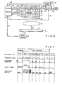
- FIGURE 6 shows an embodiment of the present invention in which the moving scene, shown by reference numeral 30 in FIGURE 6, is travelling to the right at a velocity V.
- the scene may be stationary with the camera moving or both may move.
- Radiation from the scene 30 travels along a direction generally shown by arrow 32 to the optical system of the camera shown as a lens 34 which operates to direct the radiation towards the sensor circuit or chip 38 having at the lower portion thereof CCD elements 40 identified by numbers 1, 2, 3, 4 ... K-1 and K.
- the number of CCD elements utilized in a given system is a matter of choice and the camera used in the present embodiment employed 2048 such elements.
- CCD elements 1-K are transferred periodically as shown by arrows 42 to a transfer gate 44 from whence they are transferred to a first shift register 46 by arrows such as shown at 48.
- shift register 46 produces a serial output at 50 to an amplifier 52 and from amplifier 52 along an output 54 to a selector 56.
- Selector 56 has an additional input 58 which indicates when a valid video signal exists and allows the selector to transfer the output on line 54 to a video output 60.
- the output 60 is not only a representation of the image of scene 30, but the size of the signals at output 60 is an indication of the intensity and accordingly a connection 62 is shown connected from the output 60 to an intensity sensor 64 which produces an output representative of the intensity of the signal on the video output at an output 66 which is presented to an exposure control 70.
- the intensity of radiation from scene 30 may be determined in other ways as, for example, by an intensity sensor observing the scene 30 directly.
- Exposure control 70 may comprise a computer capable of operating on the various signals to control the scan times and the exposure times as shown in connection with FIGURES 4 and 5 above.
- the input shown on conductor 66 provides the information to the exposure control 70 indicative of the intensity of radiation being received and exposure control 70 will adjust the expose time between time T l and T 2 in FIGURE 5 in accordance with that intensity.
- the speed of object 30 is sensed by a speed sensor 74 shown connected thereto by dashed line connection 76 and produces an output 78 which provides an input to exposure control 70 indicative of the speed of the object 30.
- Speed sensor 74 may be a mechanical connection that actually measures the velocity of the object 30 or the lens 34 or may be another device such as another camera which derives the speed from observing the time between two consecutive positions of points on the object. Accordingly, line 78 provides the information to the exposure control 70 to enable it to adjust the T scan time in accordance with object-camera relative speed as was explained in connection with FIGURE 4.
- the outputs of exposure control 70 are shown as outputs 80 and 82 respectively which in turn provide inputs to a first clock 86 and a second clock 88 respectively.
- the output of clock 86 is shown as output 90 presented to transfer gate 44 and the signal on output 90 operates to cause transfer gate 44 to periodically bring the charges from the CCD elements 40 to the shift register 46. This, in effect, controls the exposure time since the faster the clock pulses which exist on output 90 occur, the less time the CCD elements 40 have to integrate radiation received from object 30.
- T i is adjusted to equal S o /KI where S 0 is the desired constant intensity which may be averaged over a number of successive scans.
- the output on line 82 through clock 88 controls an output on line 92 which causes the shift register to begin transferring its information along line 50 to amplifier 52 to produce the output.
- shift register 1 can shift the signals out to amplifier 52 at various frequencies. Because the video output signal cannot exceed a frequency which the utilizing apparatus downstream can handle, a slow frequency F 2 is used when the selector 56 is set to transmit to output 60. At other times, when selector 86 dumps the output, a faster frequency F 1 may be used. The desired frequency information appears on line 92 from clock 88.
- the second shift register 94 which is set up to operate as a counter at the same frequency as shift register 46, begins producing signals on a line 96 which is presented as an additional input to exposure control 70.
- the second shift register 94 consists of a plurality of zeros except for the last shift which will be a 1 or vise versa and informs the exposure control 70 when the entire shifting process has been completed.
- the shifting out of the valid video signal from the first shift register 46 to amplifier 50 occurs at a relatively low frequency F 2 to provide a more accurate and useable output for the downstream electronics.
- FIGURE 7 shows the various timing functions involved in the circuit of FIGURE 6.
- a plurality of exposures identified as N, N+l, N+2, N+3, N+4, ... M-1 and M are shown at the top of the chart and are seen to have different lengths.
- the time between the beginning of exposure N and the end of exposure M-1 is the T scan time.
- the CCD elements are exposed to the radiation and during the remaining time, the exposure of the CCD elements is not used as is shown by the "NOT EXPOSURE" section of FIGURE 7.
- the CCD elements are receiving radiation from the moving object and integrating it.
- a transfer pulse is provided which causes the signals to be shifted into shift register 46 of FIGURE 6.
- the CCD elements 40 may again be exposed to the radiation from object 30 although until the next exposure number M, such signals will not be utilized.
- the signals stored in shift register 46 are fed out serially to amplifier 52, selector 56 and to provide a valid video output 60.
- the frequency selector pulse appearing on output 92 from clock 88 causes shift register 46 to produce its output either at a fast frequency F 1 or at a slow frequency F 2 .
- FIGURE 7 also shows the signal.from exposure control 70 along line 58 to selector 56 as the valid video signal. It is seen that during the exposure number N and the exposure numbers N+2 ... M, a not valid signal is presented to selector 56 so that the signals from the shift register 46 will not be transmitted to the video output during these times. However, during the exposure number N+l, the signal from the exposure control 70 along line 58 will allow the selector 56 to produce the video signal is shown terminating slightly before the end of exposure number N+l for purposes of assuring that no signals from the N+2 exposure are received at the video output. Since there is plenty of time for the shift register 46 to produce its output during the time N+l, the ending of the valid video signal before the ending of N+l does not provide any difficulties.
- the last graph in FIGURE 7 shows amplifier 52's output as a series of pulses of different frequencies.
- the output during exposure time N is at a fast frequency and has a slightly larger magnitude than some of the downstream outputs because it was accumulated during a time which may be slightly larger than other times.
- the valid output is shown to be at a slow frequency.and fairly large since it was accumulated during a fairly large exposure time N.
- the output at exposure number N+2 is at a fast frequency but is fairly large since it was gathered during the fairly large time N+l.
- the remaining outputs in the exposure numbers N+3, N+4 ... M are a fast frequency and relatively small since the times for N+2, N+3, N+4 are relatively small.
- the exposure control 70 After the exposure control 70 has determined the intensity of the signal from the last reading, it will know how long the exposure number N must be and since the exposure N+1 is fixed by the requirements of the shift register 46 to produce a lower frequency output, the time from the end of exposure number N+1 until the beginning of the next exposure M is determined and may vary with the speed of the object 30. Knowing the time that is available between the end of N+l and the beginning of M provides the exposure control with the ability to determine how many additional exposure numbers will be needed. Recalling that the CCD elements if left too long exposed to the radiation from object 30 may become saturated or overcharged, it is desirable to dump the charge build up on the CCD elements at a time before this happens. The time N+2, N+3, N+4, etc.
- the time for M-1(Ta) has to be almost as large as the time decided upon to utilize preventing the CCD elements from being overcharged.
- the exposure controller will determine the number of exposures after the N+l exposure in accordance with the speed of the object 30 and the intensity of the output 60.
- a line sensing CCD camera capable of observing a moving object without overlapping images of the object and in which the exposure time can be varied with intensity without there being a change in the scan time and that the scan time may be changed without there being a change in the exposure time and all without significant smearing of the image and with a useable output not obtainable in the prior art.
- Intensity sensor 64 and speed sensor 74 may be separate and independent units.
- the relative speed between the object and the camera.or a camera carrying body can be measured by optical or other radiation, e.g. by the Doppler-Shift of signals.
Landscapes
- Engineering & Computer Science (AREA)
- Multimedia (AREA)
- Signal Processing (AREA)
- Transforming Light Signals Into Electric Signals (AREA)
- Closed-Circuit Television Systems (AREA)
Applications Claiming Priority (2)
| Application Number | Priority Date | Filing Date | Title |
|---|---|---|---|
| US06/371,847 US4396950A (en) | 1982-02-26 | 1982-02-26 | CCD Camera |
| US371847 | 1982-04-26 |
Publications (2)
| Publication Number | Publication Date |
|---|---|
| EP0093077A1 true EP0093077A1 (de) | 1983-11-02 |
| EP0093077B1 EP0093077B1 (de) | 1985-12-27 |
Family
ID=23465644
Family Applications (1)
| Application Number | Title | Priority Date | Filing Date |
|---|---|---|---|
| EP83710020A Expired EP0093077B1 (de) | 1982-02-26 | 1983-04-23 | Beobachtungsvorrichtung |
Country Status (5)
| Country | Link |
|---|---|
| US (1) | US4396950A (de) |
| EP (1) | EP0093077B1 (de) |
| JP (1) | JPS59286A (de) |
| CA (1) | CA1191249A (de) |
| DE (1) | DE3361614D1 (de) |
Cited By (5)
| Publication number | Priority date | Publication date | Assignee | Title |
|---|---|---|---|---|
| GB2162019A (en) * | 1984-07-17 | 1986-01-22 | British Aerospace | Compensating for camera movement |
| FR2589301A1 (fr) * | 1985-10-28 | 1987-04-30 | I2S | Nouveaux dispositifs d'obturation electronique |
| GB2253761A (en) * | 1991-02-01 | 1992-09-16 | Samsung Electronics Co Ltd | Controlling video camera shutter speed in accordance with object speed |
| EP0458460A3 (en) * | 1990-04-23 | 1992-10-14 | Canon Kabushiki Kaisha | Photoelectric conversion apparatus |
| GB2317770A (en) * | 1982-07-14 | 1998-04-01 | British Aerospace | Solid state image sensors |
Families Citing this family (15)
| Publication number | Priority date | Publication date | Assignee | Title |
|---|---|---|---|---|
| JPS58119278A (ja) * | 1982-01-08 | 1983-07-15 | Nippon Kogaku Kk <Nikon> | 固体撮像装置 |
| JPS5995769A (ja) * | 1982-11-25 | 1984-06-01 | Hitachi Ltd | Ccdセンサ駆動装置 |
| US4591727A (en) * | 1983-11-14 | 1986-05-27 | International Business Machines Corporation | Solid state scanner for a variable speed transport |
| EP0185485A3 (de) * | 1984-12-10 | 1988-03-16 | British Aerospace Public Limited Company | Überwachungsanlagen |
| JPH0744653B2 (ja) * | 1984-12-18 | 1995-05-15 | 株式会社ニコン | 電子スチルカメラ |
| US4802024A (en) * | 1986-11-12 | 1989-01-31 | Eastman Kodak Company | Video reproduction apparatus having automatic black and white calibration |
| US4761683A (en) * | 1986-12-18 | 1988-08-02 | Xerox Corporation | Charge transfer in multiple sensor row arrays |
| EP0292253B1 (de) * | 1987-05-22 | 1992-03-18 | Oki Electric Industry Company, Limited | Bildabtaster vom Kontakt-Typ |
| JPS6449381A (en) * | 1987-08-20 | 1989-02-23 | Fuji Photo Film Co Ltd | Solid-state image pickup device |
| US4920429A (en) * | 1989-01-24 | 1990-04-24 | International Business Machines | Exposure compensation for a line scan camera |
| US5121214A (en) * | 1990-06-29 | 1992-06-09 | The United States Of America As Represented By The United States Department Of Energy | Method for eliminating artifacts in CCD imagers |
| WO1996013798A2 (en) * | 1994-10-25 | 1996-05-09 | United Parcel Service Of America, Inc. | Automatic electronic camera for label image capture |
| DK0788635T3 (da) * | 1994-10-25 | 1999-01-18 | United Parcel Service Inc | Fremgangsmåde og apparat til en bærbar kontaktløs etiketbilleddanner |
| US6806485B2 (en) | 2000-12-28 | 2004-10-19 | Valeo Electrical Systems, Inc. | Ambient light detector for off-the-glass rain sensor |
| US20040212857A1 (en) * | 2003-04-23 | 2004-10-28 | Spears Kurt E. | Control for a photosensor array |
Citations (7)
| Publication number | Priority date | Publication date | Assignee | Title |
|---|---|---|---|---|
| US3443100A (en) * | 1965-01-22 | 1969-05-06 | North American Rockwell | Apparatus for detecting moving bodies by paired images |
| DE2447299A1 (de) * | 1973-10-03 | 1975-04-17 | Tokyo Shibaura Electric Co | Ladungsuebertragungsvorrichtung |
| DE2437511A1 (de) * | 1974-08-03 | 1976-02-12 | Betr Forsch Inst Angew Forsch | Vorrichtung zur laengenmessung an sich im wesentlichen kontinuierlich bewegendem material |
| DE2810806B1 (de) * | 1978-03-13 | 1978-10-12 | Siemens Ag | Elektronische Kamera mit automatischer Einstellung der Bildhelligkeit |
| US4219845A (en) * | 1979-04-12 | 1980-08-26 | The United States Of America As Represented By The Secretary Of The Air Force | Sense and inject moving target indicator apparatus |
| US4254433A (en) * | 1979-06-25 | 1981-03-03 | General Motors Corporation | Visual motion tracking system |
| US4327378A (en) * | 1979-06-08 | 1982-04-27 | Nippon Electric Co., Ltd. | Automatic iris control for solid-stage imaging apparatus |
Family Cites Families (3)
| Publication number | Priority date | Publication date | Assignee | Title |
|---|---|---|---|---|
| US3560642A (en) * | 1967-10-13 | 1971-02-02 | Us Navy | Television satellite system |
| JPS56123183A (en) * | 1980-03-04 | 1981-09-28 | Sumitomo Metal Ind Ltd | Signal correcting method of picture data processing system |
| JPS56123184A (en) * | 1980-03-05 | 1981-09-28 | Hamamatsu Tv Kk | Observation device for moving body |
-
1982
- 1982-02-26 US US06/371,847 patent/US4396950A/en not_active Expired - Lifetime
-
1983
- 1983-04-23 EP EP83710020A patent/EP0093077B1/de not_active Expired
- 1983-04-23 DE DE8383710020T patent/DE3361614D1/de not_active Expired
- 1983-04-25 CA CA000426603A patent/CA1191249A/en not_active Expired
- 1983-04-26 JP JP58073658A patent/JPS59286A/ja active Granted
Patent Citations (7)
| Publication number | Priority date | Publication date | Assignee | Title |
|---|---|---|---|---|
| US3443100A (en) * | 1965-01-22 | 1969-05-06 | North American Rockwell | Apparatus for detecting moving bodies by paired images |
| DE2447299A1 (de) * | 1973-10-03 | 1975-04-17 | Tokyo Shibaura Electric Co | Ladungsuebertragungsvorrichtung |
| DE2437511A1 (de) * | 1974-08-03 | 1976-02-12 | Betr Forsch Inst Angew Forsch | Vorrichtung zur laengenmessung an sich im wesentlichen kontinuierlich bewegendem material |
| DE2810806B1 (de) * | 1978-03-13 | 1978-10-12 | Siemens Ag | Elektronische Kamera mit automatischer Einstellung der Bildhelligkeit |
| US4219845A (en) * | 1979-04-12 | 1980-08-26 | The United States Of America As Represented By The Secretary Of The Air Force | Sense and inject moving target indicator apparatus |
| US4327378A (en) * | 1979-06-08 | 1982-04-27 | Nippon Electric Co., Ltd. | Automatic iris control for solid-stage imaging apparatus |
| US4254433A (en) * | 1979-06-25 | 1981-03-03 | General Motors Corporation | Visual motion tracking system |
Cited By (10)
| Publication number | Priority date | Publication date | Assignee | Title |
|---|---|---|---|---|
| GB2317770A (en) * | 1982-07-14 | 1998-04-01 | British Aerospace | Solid state image sensors |
| GB2317770B (en) * | 1982-07-14 | 1998-07-15 | British Aerospace | Image sensing |
| GB2162019A (en) * | 1984-07-17 | 1986-01-22 | British Aerospace | Compensating for camera movement |
| FR2589301A1 (fr) * | 1985-10-28 | 1987-04-30 | I2S | Nouveaux dispositifs d'obturation electronique |
| EP0222641A1 (de) * | 1985-10-28 | 1987-05-20 | IMAGERIE INDUSTRIE SYSTEME Société Anonyme dite: I2S | Einrichtungen für elektronische Überblendung |
| US4851916A (en) * | 1985-10-28 | 1989-07-25 | Imagie Industrie Systeme | Electronic shutter devices |
| EP0458460A3 (en) * | 1990-04-23 | 1992-10-14 | Canon Kabushiki Kaisha | Photoelectric conversion apparatus |
| US5184006A (en) * | 1990-04-23 | 1993-02-02 | Canon Kabushiki Kaisha | Photoelectric conversion apparatus having clock signals of different frequencies |
| GB2253761A (en) * | 1991-02-01 | 1992-09-16 | Samsung Electronics Co Ltd | Controlling video camera shutter speed in accordance with object speed |
| GB2253761B (en) * | 1991-02-01 | 1995-01-11 | Samsung Electronics Co Ltd | Shutter speed control circuit |
Also Published As
| Publication number | Publication date |
|---|---|
| EP0093077B1 (de) | 1985-12-27 |
| DE3361614D1 (en) | 1986-02-06 |
| US4396950A (en) | 1983-08-02 |
| JPS59286A (ja) | 1984-01-05 |
| JPS6360597B2 (de) | 1988-11-24 |
| CA1191249A (en) | 1985-07-30 |
Similar Documents
| Publication | Publication Date | Title |
|---|---|---|
| EP0093077B1 (de) | Beobachtungsvorrichtung | |
| EP0225133B1 (de) | Verfahren zum Betrieb eines zweidimensionalen Ladungsübertragungsbildsensors | |
| JP2955715B2 (ja) | 監視装置ならびに方法 | |
| JP4530571B2 (ja) | 3次元画像検出装置 | |
| EP0142358A2 (de) | Festkörperabtastvorrichtung für einen Dokumententransport variabler Geschwindigkeit | |
| US5835137A (en) | Method and system for compensating for motion during imaging | |
| IL100106A (en) | Electro-optical imaging array with motion compensation | |
| JPS62109186A (ja) | 競技の計時装置 | |
| US4799108A (en) | Method of recording and storing images in rapid sequence | |
| US6005618A (en) | Image pick-up device with control circuit that provides a variable horizontal synchronizing signal | |
| GB2109655A (en) | Solid state image sensor | |
| US4896215A (en) | Imaging apparatus with flexible interface for controlling different image sensor types | |
| JP4398562B2 (ja) | 3次元画像検出装置の焦点調節機構 | |
| US6603512B2 (en) | Imaging apparatus and control device therefor technical field | |
| US5003398A (en) | Electronic still camera | |
| GB2184915A (en) | Imaging apparatus | |
| GB2162019A (en) | Compensating for camera movement | |
| US5548333A (en) | Color mixing prevention and color balance setting device and method for a field-sequential color television camera | |
| NL8501634A (nl) | Kamera voor televisie-, foto- respektievelijk filmopname uitgevoerd met een automatische fokusinstelinrichting. | |
| EP0456320B1 (de) | Automatische Fokussiervorrichtung | |
| JPH06319080A (ja) | プッシュブルーム走査型撮像装置 | |
| JP4391661B2 (ja) | 3次元画像検出装置 | |
| JP2001112026A (ja) | 3次元画像検出装置 | |
| JP2519202B2 (ja) | 電子的撮像装置 | |
| WO2001063910A1 (en) | Frame shuttering scheme for increased frame rate |
Legal Events
| Date | Code | Title | Description |
|---|---|---|---|
| PUAI | Public reference made under article 153(3) epc to a published international application that has entered the european phase |
Free format text: ORIGINAL CODE: 0009012 |
|
| AK | Designated contracting states |
Designated state(s): BE DE FR GB IT |
|
| 17P | Request for examination filed |
Effective date: 19840220 |
|
| GRAA | (expected) grant |
Free format text: ORIGINAL CODE: 0009210 |
|
| ITF | It: translation for a ep patent filed | ||
| AK | Designated contracting states |
Designated state(s): BE DE FR GB IT |
|
| REF | Corresponds to: |
Ref document number: 3361614 Country of ref document: DE Date of ref document: 19860206 |
|
| ET | Fr: translation filed | ||
| PLBE | No opposition filed within time limit |
Free format text: ORIGINAL CODE: 0009261 |
|
| STAA | Information on the status of an ep patent application or granted ep patent |
Free format text: STATUS: NO OPPOSITION FILED WITHIN TIME LIMIT |
|
| 26N | No opposition filed | ||
| ITTA | It: last paid annual fee | ||
| PGFP | Annual fee paid to national office [announced via postgrant information from national office to epo] |
Ref country code: FR Payment date: 19940314 Year of fee payment: 12 |
|
| PGFP | Annual fee paid to national office [announced via postgrant information from national office to epo] |
Ref country code: GB Payment date: 19940317 Year of fee payment: 12 |
|
| PGFP | Annual fee paid to national office [announced via postgrant information from national office to epo] |
Ref country code: DE Payment date: 19940319 Year of fee payment: 12 |
|
| PGFP | Annual fee paid to national office [announced via postgrant information from national office to epo] |
Ref country code: BE Payment date: 19940329 Year of fee payment: 12 |
|
| PG25 | Lapsed in a contracting state [announced via postgrant information from national office to epo] |
Ref country code: GB Effective date: 19950423 |
|
| PG25 | Lapsed in a contracting state [announced via postgrant information from national office to epo] |
Ref country code: BE Effective date: 19950430 |
|
| BERE | Be: lapsed |
Owner name: HONEYWELL INC. Effective date: 19950430 |
|
| GBPC | Gb: european patent ceased through non-payment of renewal fee |
Effective date: 19950423 |
|
| PG25 | Lapsed in a contracting state [announced via postgrant information from national office to epo] |
Ref country code: FR Effective date: 19951229 |
|
| PG25 | Lapsed in a contracting state [announced via postgrant information from national office to epo] |
Ref country code: DE Effective date: 19960103 |
|
| REG | Reference to a national code |
Ref country code: FR Ref legal event code: ST |
|
| REG | Reference to a national code |
Ref country code: HK Ref legal event code: WD Ref document number: 1012053 Country of ref document: HK |