EP0093290A2 - Connecteur à fiches pour modules à circuits intégrés - Google Patents
Connecteur à fiches pour modules à circuits intégrés Download PDFInfo
- Publication number
- EP0093290A2 EP0093290A2 EP83103572A EP83103572A EP0093290A2 EP 0093290 A2 EP0093290 A2 EP 0093290A2 EP 83103572 A EP83103572 A EP 83103572A EP 83103572 A EP83103572 A EP 83103572A EP 0093290 A2 EP0093290 A2 EP 0093290A2
- Authority
- EP
- European Patent Office
- Prior art keywords
- contact
- base
- clamping plate
- connector according
- base body
- Prior art date
- Legal status (The legal status is an assumption and is not a legal conclusion. Google has not performed a legal analysis and makes no representation as to the accuracy of the status listed.)
- Granted
Links
Images



Classifications
-
- H—ELECTRICITY
- H05—ELECTRIC TECHNIQUES NOT OTHERWISE PROVIDED FOR
- H05K—PRINTED CIRCUITS; CASINGS OR CONSTRUCTIONAL DETAILS OF ELECTRIC APPARATUS; MANUFACTURE OF ASSEMBLAGES OF ELECTRICAL COMPONENTS
- H05K7/00—Constructional details common to different types of electric apparatus
- H05K7/02—Arrangements of circuit components or wiring on supporting structure
- H05K7/10—Plug-in assemblages of components, e.g. IC sockets
- H05K7/1007—Plug-in assemblages of components, e.g. IC sockets with means for increasing contact pressure at the end of engagement of coupling parts
Definitions
- the invention relates to a connector for I.C. units according to the preamble of claim l.
- Such a connector is known for example from US Pat. No. 4,266,840.
- the connector described therein has two clamping plate parts which pivotally connect them via a separate hinge connection arranged above the clamping plate parts, so that when an IC module is inserted into the base body, the underside of the IC module presses on the swivel connection.
- the clamping plates are pressed against the base contact springs, which in turn press the connecting legs of the IC module increasingly firmly against the support surfaces formed by edge regions of the base body.
- socket bodies are aimed at, for example, electrical circuits arranged on printed circuit boards, in which a permanent and reliable function of the IC assembly is required, then it is of particular importance that firstly the IC assembly uniquely reaches the desired position and second Avoid any contact bends in the contact legs of the IC assembly.
- the base arrangements just described are not very suitable for this. Therefore, socket arrangements have been developed in which the IC assembly is first inserted into the socket and then the socket legs are clamped in place. Such arrangements are described, for example, in US Pat. No.
- 4,266,840 has the disadvantage that a separate securing device has to be provided via pawls, which prevents the clamping plates from shaking the base according to the spring forces acting on them from the unstable holding state to the more stable one Swing open the release state and thus the IC assembly in would release their contact to the socket contacts.
- latch locking is a further disadvantage that a simple and inexpensive base construction prohibits.
- a particular advantage of the invention can be seen in the fact that the new connector can also be used for the subsequent assembly of already existing printed circuits, because when a damaged IC component is unsoldered, the new connector can be soldered in its place and the others become Printed circuit elements not at risk from repeated soldering. A further exchange of the individual IC components is then possible simply by opening and closing the socket contacts. However, this presupposes that the dimensions of the new connector essentially correspond to those of the IC module itself and, moreover, the base contacts have solder pins or wrap connections which correspond in their arrangement to the arrangement of the connection legs of an IC module.
- the solder pin of the new plug is particularly advantageous connector with a square cross-section selected, because this means that the base cannot "float" during automatic soldering in a solder bath, because the liquid solder finds enough space between the side walls of the square cross-sectional soldering pin and the round hole in the circuit board to penetrate and thus to prevent floating.
- Another significant advantage of the invention is that the new connector can hold the IC module securely even when shaken, since the clamping plates have a stable position in the locking position, and should only be transferred to the even more spring-loaded clamping position when shaken that they can move from the unstable clamping position to a stable release position again.
- a particularly simple yet extremely effective securing of the I.C. units used is achieved.
- the hinge connection between the clamping plate parts has a swivel angle limitation, so that the spring forces acting in the released position on the outer clamping plate edges hold the clamping plate device in a clamped arrangement in the base device.
- the outer edges of the clamping plate are held directly by the spring contacts and by separately designed retaining profile elements, which would be both constructive and costly.
- the holding profiles and the shape of the outer clamping plate edges are formed in the shape of an arc segment or even in the form of a circular segment, so that the clamping plate edges can serve as bearings and the spring elements can serve as bearing shells.
- an actuating pin which can also be arranged on both sides, is advantageously formed on at least one end face of the clamping plate parts.
- the selected construction of the hinge parts formed on the clamping plates and / or the hinge pin of the swivel connection is particularly advantageous.
- the locking position only has to be formed by a stop point for the clamping plate device on the top of the base body, the provision of a corresponding stop on the top of the base body would in principle be sufficient for this purpose.
- the formation of these clamping plate contact surfaces can already be taken into account during the production of the clamping plate body in the printing or spraying process without significant additional tool costs.
- the design of the base contacts which can be pressed into the base body largely or in one piece. Since the upper end areas of the base contacts are designed as spring tongues, they deliver the desired spring pressure on the outer clamping plate edges. In order to be able to insert the spring tongues with the base contacts under a corresponding pretension in the base body, it is particularly advantageous if a spring tongue contact surface is formed on the top of the base body, which can extend into the base body in the form of a notch. It is sufficient if the spring tongue with the tongue-F Eder bearing surface a small angle, which determines the amount of travel substantially.
- the contact legs of the I.C. assembly are pressed by the spring tongue against a support surface, which is formed by a raised edge of the base body.
- This raised edge can advantageously have a run-in slope that facilitates the insertion of the I.C. assembly into the base.
- the support surface is formed by a support contact which is formed at the upper end region of the base contact with the latter, so that the upper end region of the base contact consists on the one hand of the spring tongue and on the other hand of the support contact.
- a tulip-like solution can be selected for the upper end region of the base contact, in which part of the base contact is formed as a spring tongue by means of two corresponding incisions. If particularly high retention forces are desired, then the support contact is largely solid with the base contact and a separate spring tongue is connected to the base contact, so that the spring tongue extends from the lower end region through the middle holding region into the upper end region of the base contact.
- the support contact can then advantageously have a head section which gives the support contact a further strength in the upper region and which has a nose-shaped contact surface, as a result of which a more punctiform and less flat load occurs, which leads to more intensive contact between the contact leg of the IC Unit and the base contact leads.
- the support contact is in addition to the elasticity modules in the clamping plate and essentially Lichen achieved another elastic moment in the spring tongue. This is particularly important because, due to the small construction dimensions, all parts of the new connector have to be used functionally.
- the support contact meets a support contact contact surface at a short distance, which can be formed in the edge of the base body and thus on the one hand prevents the support contacts from being overstretched when inserting IC modules or when fiddling with the contacts, and on the other hand the risk of Prevents contact with a neighboring contact of the neighboring base.
- the new connector can also be configured with test socket brackets to form a pronounced test socket connector, in that the new connector is only provided with actuating pins, which are advantageously the hinge pins that extend into a corresponding lever device of a test socket.
- the new connector can also be used for the test socket area, which is a further advantage for a uniform connector design.
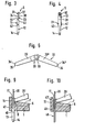
- a base body 1 has an underside 2, an upper side 3 and lateral long sides 4.
- the upper side 3 of the base body 1 is covered between a base plate contact 5 inserted into the base body 1 by a clamping plate contact surface section 6, on the free upper side of which the clamping plate contact surface 7 is formed.
- the clamping plate contact surface 7 is V-shaped from the center of the base body and includes an obtuse angle ⁇ of cica 165 0 .
- the angle ⁇ depending on the purpose of the socket body for a range of 180 0 and 150 ° exert the same 'function according to the invention.
- a spring tongue contact surface 9 which extends relatively steeply downwards to the base top 3, where the base contact 5 has an upper end region 10 from the base body top. 3 protrudes, while a central holding area 11 of the base contact 5 is fixed with a press fit in the base body 1.
- a lower end region 12 of the base contact 5 protrudes vertically downward and merges into a solder connection pin 13 which is square in cross section and has a tip 14 which, for easier insertion of the solder connection pin 13, for example for the bores of PCB holes.
- the longitudinal sides 4 of the base body 1 merge into a base edge 15, which has an inlet bevel 17 on its upper end face 16, which points obliquely downwards from the upper end face 16 towards the center of the base and extends to an inner base edge side surface 18, as shown in particular in FIG 7 shown.
- the inner side edge 18 serves as a support surface 19 for a connecting leg 20 in the IC module 21, which is inserted into the base 1 and by a clamping device 22 according to the form of illustration in FIG. 2 with the back surface 24 of a spring tongue 23 is clamped against the inner side edge 18 of the base edge 15.
- FIG. 1 shows the clamping device 22 composed of a left clamping plate part 25 ′ and a right clamping plate part 25 ′′ in the release position 26 with solid lines and a clamping position 27 with dashed lines, while a locking position 28, which also corresponds to the operating position in FIG. 2 is shown.
- the clamping device 22 has a pivotal connection 29, which "'connects via hinge axis detents 30.
- the two clamp parts 25 and 25' and 25" the two clamp parts 25 a formed in the area of the Gelenkachsen.rasten 30 Schwenkwegbegrenzung 31 which ig according to F in the release position, the 26th, each limited by mutual abutment 1 the pivoting about the release position out.
- the two clamping plate parts 25 'and 25''an upper swivel path limitation 32 is provided, which can limit a swivel path downward beyond the locking position 28, because this enables better work preparation during the manufacture and assembly of the clamping device 22.
- the outer clamping plate edges 34 'and 34'' have a preferably circular arc shape 35 which is at least partially the circular arc contour 37 of the Haltpro correspond to fil elements 36 and rest on a front surface 38 of the spring tongue 23. Projections 39 - as shown in FIG. 6 - are provided between the outer clamping plate edges 34 'and 34 "and extend between the base contacts 5.
- a single base contact 5 is shown in a transverse view, and according to FIG. 4 the same base contact 5 is shown in a longitudinal view, wherein transverse grooves 40 can clearly be seen which cooperate with the connecting legs 20 of the I.C. assembly 21. 4 that anchoring hooks 41 are provided, with which the base contact 5 can additionally be anchored in the base body 1 in its press fit.
- anchoring hooks 41 are provided, with which the base contact 5 can additionally be anchored in the base body 1 in its press fit.
- the base contact 5 merges into the lower end region 12, where a transition shoulder 42 merges into a square cross section.
- the spring tongue 23 extends according to FIG.
- the spring tongue 23 is designed as a holding profile element 36 with the curved contour 37, as is also shown in FIG. 3.
- FIG. 5 again shows the clamping device 22 in the release position 26, how the clamping device 22 is inserted into the base body 1 before assembly and then has the position according to FIG. 1 in solid lines.
- the base body 1 is shown without base contacts 5 and clamping device 22.
- the raised base edge 15 with the associated run-in slope 17 is shown more clearly.
- the receiving chambers 45 can be seen, in which the base contacts 5 are inserted.
- FIG. 8 shows a top view of the base body 1 according to FIG. 7, in which the receiving chambers 45 and the inlet slope 17 can be seen in a top view. Likewise, the spaces between the individual receiving chambers 45 are shown, into which the clamping plate projections 39 engage and thus prevent the clamping device 22 from slipping in the longitudinal direction of the base.
- FIG. 9 shows another embodiment of a base contact 46, in which the inner side edge 18 is covered by a support contact 47, so that the connecting leg 20 of the IC module 21 is not clamped against the inner side edge 18 but against the support contact 47, which thereby forms the function of the support surface 19. Since the support contact 47 partially fills the contact space 44, the play for the connecting leg 20 of the I.C. assembly 21 when inserting the connecting leg 20 is considerably restricted. The support contact 47 is pulled up to the run-in slope 17, so that the connecting legs 20 get stuck when the I.C. assembly 21 is inserted, thereby reducing the risk of damage.
- FIG. 10 shows a further embodiment for another base contact 48, in which a support contact is also provided and the base contact 48 and the support contact 47 have a tulip-shaped configuration, the tulip base 49 projecting into the base body 1 and thus having a lower overall height for the base body equipped with the IC component is reached.
- the base contact 48 is longitudinally divided, while the base contact 46 according to FIG. 9 has the same embodiment as the base contact 5 and is only supplemented by the support contact 47.
- the support contact 50 is designed as a main contact and the spring tongue 23 has one in the middle holding area 11 to the lower one End area 12 reaching extension.
- the spring tongue 23 is riveted or welded to the solid support contact 50.
- the support contact 50 can also be formed in one piece with the spring tongue 23.
- the clamping plate contact surface 7 is extended somewhat further into the contact surface / m 44 than is the case in the embodiment according to FIG. 1, where the clamping plate contact surface 7 merges into a curve after the outer boundary line 8, as can be clearly seen in FIG. 7.
- FIG. 11 the clamping plate contact surface 7 is extended somewhat further into the contact surface / m 44 than is the case in the embodiment according to FIG. 1, where the clamping plate contact surface 7 merges into a curve after the outer boundary line 8, as can be clearly seen in FIG. 7.
- the spring tongue contact surface 9 therefore extends from the top 3 of the base body 1 to the clamping plate contact surface 7 in a flat course.
- the spring tongue bearing surface 9 forms with the front face 38 of the spring tongue 23 forms an acute angle ⁇ , which is in the order of 0 ° to about 30 and preferably 0 15 0 depending on the position of the clamping device 22nd
- the base edge 15 also has a support contact bearing surface 51, which includes an acute angle ⁇ with a rear side 52 of the support contact 50. The amounts depending on the load of the support contact between> 0 ° and about 30 0, preferably 15 °.
- the contact surface 51 essentially serves to prevent the support contact 50 from being bent beyond the outer longitudinal side 4 of the base body 1 and thus to introduce the risk that an undesired power connection will be established with the corresponding support contact 50 of a neighboring base.
- the support contact 50 has a head region 53 which, like the base edge 15 in accordance with the embodiment of FIG. 1, has an inlet slope 17.
- the run-in slope 17 merges into a nose projection 54 which carries on its front side the supporting surface 19 or a contact zone which can exert a more punctiform load on the connecting leg 20 of an IC module 21.
- the support contact 50 thus takes the main compressive forces on the connecting leg 20 with it a certain range of elasticity, while the spring tongue 23 initially the; Main spring travel forms and then transmits the essential compressive forces of the clamping device 22 from the clamping plate parts 25 through the solid material of the spring tongue 23 from the front surface 38 to the back surface 24 and thus to the connecting leg 20.
- the spring tongue 23 thus has an auxiliary contact and a holding profile function, the main function of course being the introduction of the spring forces for the clamping device.
- the contact space 44 is delimited laterally and downwards by the tulip floor 49 by the back surface 24 of the spring tongue 23 and by the front surface of the support contact 50.
- the base body 1 is formed in one piece, that is to say with the clamping plate contact surface section 6 and the base edge 15 in one piece, then an indentation is formed by the spring tongue contact surface 9 on the one side and the support contact contact surface 51 on the base edge side, in which the spring tongue 23 and the support contact 50 composite socket contact 55 can be used.
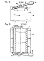
- a test base 56 which has a lever device 57.
- a recess 59 is provided in the actuating lever 58, into which an actuating pin 60 protrudes.
- the actuating pin 60 can be the articulated axis catch 30, which either extends directly or protrudes into the recess 59 via a driver 61 and thus enables the clamping device 22 to be pivoted from the release position via the clamping position 27 into the locking position 28 and back via the actuating lever 58.
- FIG. 13 shows a top view of the device according to FIG. 12, which essentially corresponds to the top view of the illustration according to FIG. 6, in which the actuating lugs 62 with associated locking bolts 63 are also provided.
- the locking bolts 63 can be formed on a clamping plate part 25 'in a small projection curvature, so that they can snap into holes 64 of the actuating lugs 62 due to an elastic deformation of the actuating lugs 62 when they are joined together.
- the actuating lugs 62 are formed in the clamping plate part 25 ′′.
- articulated axis pins 30 can then be inserted, which extend into the lever device 57 in their extension, or in another embodiment a pin of the lever device 57 is inserted into the bore 64 of the actuating lug 62.
- plug connectors or bases which are suitable for series production can be created, which can be easily produced from insulating material and which base contacts can be pressed into the contact chambers provided therein. Since the packing density of the semiconductors requires a small size of the base body, they must be arranged in rows from four sides, which is only possible with a base according to the present invention. Since very high demands are made on the electrical and mechanical properties, miniature contacts with pretensioned contact springs must be found in the limited space available.
- the spring contacts can lose their holding force due to secondary natural vibrations, so that the semiconductors can fall out of the base holder or at least contact fluctuations can result.
- This is an intolerable disadvantage, especially in aerospace applications as well as in electroplating and in other important application areas, which is avoided by the present invention.
- the long-term function Soft contact springs for IC components under environmental influences such as heat, cold, aggressive industrial atmosphere, air humidity, etc. are often not guaranteed.
- the underside of the base should be absolutely solder-tight and the soldering pins should be designed so that there is no risk of floating during automatic soldering in the solder bath.
- the simple shape also contributes to the fact that the contact is already securely fulfilled in the upper region of the contact leg and, thanks to the transverse grooves in the contact region of the contact leg, also an absolutely reliable contact even with oxidized connecting plugs guaranteed. Since the contact is continuously formed in one piece, transition losses can be avoided and there is no risk of being stuck through the firm contact with the clamping plates or at the base edge.
Landscapes
- Engineering & Computer Science (AREA)
- Microelectronics & Electronic Packaging (AREA)
- Connecting Device With Holders (AREA)
- Details Of Connecting Devices For Male And Female Coupling (AREA)
- Coupling Device And Connection With Printed Circuit (AREA)
Priority Applications (1)
| Application Number | Priority Date | Filing Date | Title |
|---|---|---|---|
| AT83103572T ATE24648T1 (de) | 1982-04-21 | 1983-04-13 | Steckverbinder fuer i.c.-baueinheiten. |
Applications Claiming Priority (4)
| Application Number | Priority Date | Filing Date | Title |
|---|---|---|---|
| DE19823214841 DE3214841C2 (de) | 1982-04-21 | 1982-04-21 | Steckverbinder für I.C.-Baueinheiten |
| DE3214841 | 1982-04-21 | ||
| DE19838305384 DE8305384U1 (de) | 1983-02-25 | 1983-02-25 | Steckverbinder für IC-Baueinheiten |
| DE8305384U | 1983-02-25 |
Publications (3)
| Publication Number | Publication Date |
|---|---|
| EP0093290A2 true EP0093290A2 (fr) | 1983-11-09 |
| EP0093290A3 EP0093290A3 (en) | 1984-09-12 |
| EP0093290B1 EP0093290B1 (fr) | 1986-12-30 |
Family
ID=25801251
Family Applications (1)
| Application Number | Title | Priority Date | Filing Date |
|---|---|---|---|
| EP83103572A Expired EP0093290B1 (fr) | 1982-04-21 | 1983-04-13 | Connecteur à fiches pour modules à circuits intégrés |
Country Status (3)
| Country | Link |
|---|---|
| US (1) | US4509812A (fr) |
| EP (1) | EP0093290B1 (fr) |
| DE (1) | DE3368843D1 (fr) |
Families Citing this family (9)
| Publication number | Priority date | Publication date | Assignee | Title |
|---|---|---|---|---|
| DE3543955A1 (de) * | 1985-12-12 | 1987-06-19 | Karl Lotter | Steckverbinder fuer ic-baueinheiten |
| US4761141A (en) * | 1987-03-03 | 1988-08-02 | Amp Incorporated | Locking latching shroud |
| US4919623A (en) * | 1989-02-13 | 1990-04-24 | Amp Incorporated | Burn-in socket for integrated circuit device |
| US5147213A (en) * | 1991-10-24 | 1992-09-15 | Minnesota Mining And Manufacturing Company | Zero insertion pressure test socket for pin grid array electronic packages |
| JP3256796B2 (ja) * | 1994-08-23 | 2002-02-12 | 日本テキサス・インスツルメンツ株式会社 | ソケット及びソケットを用いた電気部品の試験方法 |
| US5597320A (en) * | 1995-01-03 | 1997-01-28 | Molex Incorporated | Zero insertion force electrical connector and terminal |
| US5498970A (en) * | 1995-02-06 | 1996-03-12 | Minnesota Mining And Manufacturing | Top load socket for ball grid array devices |
| DE19511509C2 (de) * | 1995-03-29 | 1999-05-12 | Siemens Ag | Elektrischer Leiterplattenverbinder |
| TWI368007B (en) * | 2009-06-26 | 2012-07-11 | Delta Electronics Inc | Assembled structure of electronic device and supporting device thereof |
Family Cites Families (14)
| Publication number | Priority date | Publication date | Assignee | Title |
|---|---|---|---|---|
| US2825037A (en) * | 1955-02-04 | 1958-02-25 | Harry H French | Printed-circuit card clamp |
| US3130351A (en) * | 1961-09-14 | 1964-04-21 | George J Giel | Modular circuitry apparatus |
| GB1371030A (en) * | 1970-08-18 | 1974-10-23 | Sdc Products Electronics Ltd | Plug and socket connectors and sockets therefor |
| GB1405417A (en) * | 1971-11-19 | 1975-09-10 | Carr Fastener Co Ltd | Electrical connection sockets |
| US3883207A (en) * | 1973-09-13 | 1975-05-13 | Molex Inc | Low insertion force connector for modular circuit packages |
| NL7505939A (nl) * | 1975-05-21 | 1976-11-23 | Du Pont | Contactinrichting voor geintegreerde ketens. |
| US3997227A (en) * | 1975-07-28 | 1976-12-14 | Cutchaw John M | Connector and handling device for multilead electronic packages |
| US4189176A (en) * | 1978-07-05 | 1980-02-19 | Hamilton William J | Latch bolt accessory |
| US4193656A (en) * | 1978-12-20 | 1980-03-18 | Amp Incorporated | Extraction device for extracting a DIP from a DIP header |
| US4266839A (en) * | 1979-07-06 | 1981-05-12 | E. I. Du Pont De Nemours And Company | Zero insertion force toggle link connector |
| US4266840A (en) * | 1979-10-29 | 1981-05-12 | Jack Seidler | Circuit holder |
| US4375309A (en) * | 1980-12-24 | 1983-03-01 | Wells Electronics, Inc. | Zero insertion force connector block |
| US4407555A (en) * | 1981-03-19 | 1983-10-04 | Amp Incorporated | Cam actuated DIP test socket |
| US4402563A (en) * | 1981-05-26 | 1983-09-06 | Aries Electronics, Inc. | Zero insertion force connector |
-
1983
- 1983-03-07 US US06/472,844 patent/US4509812A/en not_active Expired - Fee Related
- 1983-04-13 EP EP83103572A patent/EP0093290B1/fr not_active Expired
- 1983-04-13 DE DE8383103572T patent/DE3368843D1/de not_active Expired
Also Published As
| Publication number | Publication date |
|---|---|
| DE3368843D1 (en) | 1987-02-05 |
| EP0093290B1 (fr) | 1986-12-30 |
| US4509812A (en) | 1985-04-09 |
| EP0093290A3 (en) | 1984-09-12 |
Similar Documents
| Publication | Publication Date | Title |
|---|---|---|
| DE3872312T2 (de) | Pruefsockel mit verbesserter kontakteinrastung. | |
| EP2255412B1 (fr) | Dispositif de connexion électrique | |
| DE2355774C2 (de) | Elektrischer Verbinder, insbesondere Steckverbinder, für elektrische Flachkabel mit Kunststoffisolation | |
| DE69502108T2 (de) | Kugelrasterbuchsegehaüse | |
| DE69531165T2 (de) | Elektrischer verbinder | |
| DE69705981T2 (de) | Verbinder mit verstärkter Verriegelung | |
| DE60111141T2 (de) | Batteriehalter zum Festhalten einer flachen Batterie | |
| EP1231679A1 (fr) | Connecteur composé d'une pièce male et femelle | |
| DE69935181T2 (de) | Sockel für elektrische Teile | |
| DE2203435A1 (de) | Elektrisches Verbinderelement fuer gedruckte Schaltungen | |
| DE2409075A1 (de) | Elektrischer verbinder | |
| EP3375048B1 (fr) | Contact à enficher | |
| EP3446367B1 (fr) | Contact enfichable | |
| DE69410575T2 (de) | Elektrische Verbinderanordnung zum Montieren auf gedruckte Leiterplatten | |
| EP0093290B1 (fr) | Connecteur à fiches pour modules à circuits intégrés | |
| DE69409662T2 (de) | Elektrischer verbinder zur oberflächenmontage auf einer leiterplatte | |
| DE102018000940A1 (de) | Steckverbinder und Kontaktanordnung | |
| EP0828320A1 (fr) | Connecteur | |
| WO1989006447A1 (fr) | Systeme de couplage amovible, notamment de deux plaquettes de circuits imprimes, et plaquettes appropriees de circuits imprimes | |
| DE19816502A1 (de) | Elektrische Anschlußklemme | |
| EP0702426A1 (fr) | Contact à insertion à force | |
| DE3214841C2 (de) | Steckverbinder für I.C.-Baueinheiten | |
| DE4221689A1 (de) | Elektronikmodul-sockel mit federnd nachgiebigem verriegelungsglied | |
| EP4035226B1 (fr) | Aide au montage | |
| DE102008046567B3 (de) | Steckverbinder zum Anschließen eines elektrischen Leiters an eine Leiterplatte |
Legal Events
| Date | Code | Title | Description |
|---|---|---|---|
| PUAI | Public reference made under article 153(3) epc to a published international application that has entered the european phase |
Free format text: ORIGINAL CODE: 0009012 |
|
| 17P | Request for examination filed |
Effective date: 19830427 |
|
| AK | Designated contracting states |
Designated state(s): AT BE CH DE FR GB IT LI LU NL SE |
|
| PUAL | Search report despatched |
Free format text: ORIGINAL CODE: 0009013 |
|
| AK | Designated contracting states |
Designated state(s): AT BE CH DE FR GB IT LI LU NL SE |
|
| 17Q | First examination report despatched |
Effective date: 19860116 |
|
| GRAA | (expected) grant |
Free format text: ORIGINAL CODE: 0009210 |
|
| AK | Designated contracting states |
Kind code of ref document: B1 Designated state(s): AT BE CH DE FR GB IT LI LU NL SE |
|
| REF | Corresponds to: |
Ref document number: 24648 Country of ref document: AT Date of ref document: 19870115 Kind code of ref document: T |
|
| PG25 | Lapsed in a contracting state [announced via postgrant information from national office to epo] |
Ref country code: SE Effective date: 19861231 |
|
| ET | Fr: translation filed | ||
| REF | Corresponds to: |
Ref document number: 3368843 Country of ref document: DE Date of ref document: 19870205 |
|
| ITF | It: translation for a ep patent filed | ||
| PG25 | Lapsed in a contracting state [announced via postgrant information from national office to epo] |
Ref country code: LU Free format text: LAPSE BECAUSE OF NON-PAYMENT OF DUE FEES Effective date: 19870430 |
|
| PGFP | Annual fee paid to national office [announced via postgrant information from national office to epo] |
Ref country code: NL Payment date: 19870430 Year of fee payment: 5 |
|
| PLBE | No opposition filed within time limit |
Free format text: ORIGINAL CODE: 0009261 |
|
| STAA | Information on the status of an ep patent application or granted ep patent |
Free format text: STATUS: NO OPPOSITION FILED WITHIN TIME LIMIT |
|
| 26N | No opposition filed | ||
| PG25 | Lapsed in a contracting state [announced via postgrant information from national office to epo] |
Ref country code: AT Effective date: 19880413 |
|
| PG25 | Lapsed in a contracting state [announced via postgrant information from national office to epo] |
Ref country code: LI Effective date: 19880430 Ref country code: CH Effective date: 19880430 |
|
| BERE | Be: lapsed |
Owner name: LOTTER KARL Effective date: 19880430 |
|
| PG25 | Lapsed in a contracting state [announced via postgrant information from national office to epo] |
Ref country code: NL Effective date: 19881101 |
|
| NLV4 | Nl: lapsed or anulled due to non-payment of the annual fee | ||
| REG | Reference to a national code |
Ref country code: CH Ref legal event code: PL |
|
| PG25 | Lapsed in a contracting state [announced via postgrant information from national office to epo] |
Ref country code: BE Effective date: 19890430 |
|
| PGFP | Annual fee paid to national office [announced via postgrant information from national office to epo] |
Ref country code: FR Payment date: 19910326 Year of fee payment: 9 |
|
| PGFP | Annual fee paid to national office [announced via postgrant information from national office to epo] |
Ref country code: GB Payment date: 19910402 Year of fee payment: 9 |
|
| ITTA | It: last paid annual fee | ||
| PG25 | Lapsed in a contracting state [announced via postgrant information from national office to epo] |
Ref country code: GB Effective date: 19920413 |
|
| PGFP | Annual fee paid to national office [announced via postgrant information from national office to epo] |
Ref country code: DE Payment date: 19920522 Year of fee payment: 10 |
|
| GBPC | Gb: european patent ceased through non-payment of renewal fee | ||
| PG25 | Lapsed in a contracting state [announced via postgrant information from national office to epo] |
Ref country code: FR Effective date: 19921230 |
|
| REG | Reference to a national code |
Ref country code: FR Ref legal event code: ST |
|
| PG25 | Lapsed in a contracting state [announced via postgrant information from national office to epo] |
Ref country code: DE Effective date: 19940101 |