EP0093890A2 - Apparat zur Detektion von Oberflächenunregelmässigkeiten auf einem strangförmigen Material - Google Patents
Apparat zur Detektion von Oberflächenunregelmässigkeiten auf einem strangförmigen Material Download PDFInfo
- Publication number
- EP0093890A2 EP0093890A2 EP83103627A EP83103627A EP0093890A2 EP 0093890 A2 EP0093890 A2 EP 0093890A2 EP 83103627 A EP83103627 A EP 83103627A EP 83103627 A EP83103627 A EP 83103627A EP 0093890 A2 EP0093890 A2 EP 0093890A2
- Authority
- EP
- European Patent Office
- Prior art keywords
- linear material
- photoelectric conversion
- conversion elements
- light
- irregularities
- Prior art date
- Legal status (The legal status is an assumption and is not a legal conclusion. Google has not performed a legal analysis and makes no representation as to the accuracy of the status listed.)
- Granted
Links
Images
Classifications
-
- G—PHYSICS
- G01—MEASURING; TESTING
- G01N—INVESTIGATING OR ANALYSING MATERIALS BY DETERMINING THEIR CHEMICAL OR PHYSICAL PROPERTIES
- G01N21/00—Investigating or analysing materials by the use of optical means, i.e. using sub-millimetre waves, infrared, visible or ultraviolet light
- G01N21/84—Systems specially adapted for particular applications
- G01N21/88—Investigating the presence of flaws or contamination
- G01N21/95—Investigating the presence of flaws or contamination characterised by the material or shape of the object to be examined
- G01N21/952—Inspecting the exterior surface of cylindrical bodies or wires
-
- G—PHYSICS
- G01—MEASURING; TESTING
- G01B—MEASURING LENGTH, THICKNESS OR SIMILAR LINEAR DIMENSIONS; MEASURING ANGLES; MEASURING AREAS; MEASURING IRREGULARITIES OF SURFACES OR CONTOURS
- G01B11/00—Measuring arrangements characterised by the use of optical techniques
- G01B11/08—Measuring arrangements characterised by the use of optical techniques for measuring diameters
- G01B11/10—Measuring arrangements characterised by the use of optical techniques for measuring diameters of objects while moving
-
- G—PHYSICS
- G01—MEASURING; TESTING
- G01N—INVESTIGATING OR ANALYSING MATERIALS BY DETERMINING THEIR CHEMICAL OR PHYSICAL PROPERTIES
- G01N21/00—Investigating or analysing materials by the use of optical means, i.e. using sub-millimetre waves, infrared, visible or ultraviolet light
- G01N21/84—Systems specially adapted for particular applications
- G01N21/88—Investigating the presence of flaws or contamination
Definitions
- the present invention relates to an apparatus for detecting any irregularities on the surface of a linear material in a continuous and non-contact manner.
- apparatus for detecting any irregularities on the surface of a linear material comprising a light projector for projecting a parallel light on said material and a light receptor for receiving said light and the shadow of said material travelling between said light projector and said light receptor, said light receptor comprising a pair of photoelectric conversion elements arranged with a space therebetween on a line parallel to the path of said material, the longitudinal sides of said photoelectric conversion elements being longer than the width of the shadow of said linear material cast on said elements and being perpendicular to the direction in which said material travels, and a differential amplifier connected to said photoelectric elements for determining the difference between the electrical outputs from said photoelectric conversion elements, whereby detecting any irregularities on the surface of said linear material.
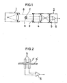
- the detector in accordance with the present invention includes a light projector 1 adapted to emit a parallel light a and a light receptor 2 opposed to the light projector.
- a linear material b to be tested travels therebetween in a direction perpendicular to the parallel light a.
- a transmissive screen 3 is provided on the front of the light receptor 2.
- a lens 4 and a pair of photoelectric conversion elements 5 are provided behind the screen 3. The shadow b' of the linear material b is cast on the screen 3 and focussed by the lens 4 on the surfaces of the photoelectric conversion elements 5.
- the photoelectric conversion elements 5 are longer than the width of the shadow b' of the linear material. They are arranged with a space therebetween on a line parallel to the path of said material. Their longitudinal edges are perpendicular to the direction in which the linear material travels. The elements 5 are so long that even if the linear material b oscillates up and down, the shadow b' will not get off the two photoelectric conversion elements disposed in parallel with each other. The output terminals of these elements 5 are connected to the input terminals of a differential amplifier 6.
- the screen 3 and the lens 4 may be omitted from the light receptor 2.
- the parallel light a and the shadow b' of the linear material may be directly cast on the photoelectric conversion elements 5.
- a plurality of detectors may be provided around the linear material b if it is required to detect surface irregularities over its whole periphery.
- the shadow c' of the irregularity is cast on the photoelectric conversion elements 5. This causes a difference between the area of the shadow of the linear material which is cast on one element 5 and that which is cast on the other element 5. This causes a difference between the electrical output of one element and that of the other element.
- This difference in the output is amplified by the differential amplifier 6 and given to an alarm. An observer is notified by the alarm if the output of the differential amplifier 6 exceeds a predetermined level.
- any irregularities on the surface of a running linear meterial can be continuously detected because a pair of photoelectric conversion elements are disposed with a space left therebetween, perpendicular to the direction in which the linear material travels. If there is an irregularity on the surface of the linear material, it is detected in terms of a difference in the electrical output.
- the apparatus in accordance with the present invention is not affected by vibration if the photoelectric conversion elements have such a sufficient length that, even if the linear material oscillates up and down, the shadow thereof will not get off the photoelectric conversion elements. Because the signal outputs of the photoelectric conversion elements have no relation to the diameter of the linear material, the apparatus in accordance with the present invention need not be adjusted even if the diameter of the linear material has changed. Also, the apparatus in accordance with the present invention is not affected by a change in the speed at which the linear material travels.
Landscapes
- Physics & Mathematics (AREA)
- General Physics & Mathematics (AREA)
- General Health & Medical Sciences (AREA)
- Chemical & Material Sciences (AREA)
- Analytical Chemistry (AREA)
- Biochemistry (AREA)
- Life Sciences & Earth Sciences (AREA)
- Health & Medical Sciences (AREA)
- Immunology (AREA)
- Pathology (AREA)
- Length Measuring Devices By Optical Means (AREA)
- Filamentary Materials, Packages, And Safety Devices Therefor (AREA)
- Geophysics And Detection Of Objects (AREA)
- Investigating Materials By The Use Of Optical Means Adapted For Particular Applications (AREA)
Applications Claiming Priority (2)
| Application Number | Priority Date | Filing Date | Title |
|---|---|---|---|
| JP78644/82 | 1982-05-10 | ||
| JP57078644A JPS58207254A (ja) | 1982-05-10 | 1982-05-10 | 線条体表面の凹凸検出装置 |
Publications (3)
| Publication Number | Publication Date |
|---|---|
| EP0093890A2 true EP0093890A2 (de) | 1983-11-16 |
| EP0093890A3 EP0093890A3 (en) | 1984-08-15 |
| EP0093890B1 EP0093890B1 (de) | 1987-07-01 |
Family
ID=13667568
Family Applications (1)
| Application Number | Title | Priority Date | Filing Date |
|---|---|---|---|
| EP83103627A Expired EP0093890B1 (de) | 1982-05-10 | 1983-04-14 | Apparat zur Detektion von Oberflächenunregelmässigkeiten auf einem strangförmigen Material |
Country Status (5)
| Country | Link |
|---|---|
| EP (1) | EP0093890B1 (de) |
| JP (1) | JPS58207254A (de) |
| KR (1) | KR870000477B1 (de) |
| CA (1) | CA1203597A (de) |
| DE (1) | DE3372306D1 (de) |
Cited By (4)
| Publication number | Priority date | Publication date | Assignee | Title |
|---|---|---|---|---|
| GB2174804A (en) * | 1985-04-26 | 1986-11-12 | Koerber Ag | Monitoring the condition of filamentary belts in cigarette making machines and the like |
| EP0334544A3 (de) * | 1988-03-19 | 1990-09-26 | Cabot Plastics Limited | Verfahren und Vorrichtung zur Oberflächenzustandsauswertung eines Gegenstandes |
| EP1643246A1 (de) * | 2004-10-01 | 2006-04-05 | Barco NV | Kompakter Fasermaterialdetektor |
| WO2006115007A1 (ja) | 2005-04-21 | 2006-11-02 | Sumitomo Electric Industries, Ltd. | 超電導線材の検査装置および検査方法 |
Families Citing this family (2)
| Publication number | Priority date | Publication date | Assignee | Title |
|---|---|---|---|---|
| DE19958993A1 (de) * | 1999-12-07 | 2001-06-28 | Christoph Berthold | Anordnung zur zerstörungsfreien und berührungslosen Produktionsüberwachung der Dicke und/oder der Geometrie von Fasern in allen Bereichen der Faserproduktion mit Hilfe der Lichtstreuung |
| JP2023180625A (ja) * | 2022-06-10 | 2023-12-21 | 日本ケーブル株式会社 | 索条のスプライス部検出装置 |
Family Cites Families (4)
| Publication number | Priority date | Publication date | Assignee | Title |
|---|---|---|---|---|
| US4007992A (en) * | 1975-06-02 | 1977-02-15 | Techmet Company | Light beam shape control in optical measuring apparatus |
| GB1525157A (en) * | 1975-08-06 | 1978-09-20 | Ellenberger & Poensgen | Multi-pole excess current circuit breaker |
| FR2389099A1 (fr) * | 1977-04-25 | 1978-11-24 | Sopelem | Procede optique de controle dimensionnel |
| JPS54146656A (en) * | 1978-05-08 | 1979-11-16 | Kobe Steel Ltd | Method and device for measuring quantity of bend of rod |
-
1982
- 1982-05-10 JP JP57078644A patent/JPS58207254A/ja active Pending
-
1983
- 1983-04-12 KR KR1019830001511A patent/KR870000477B1/ko not_active Expired
- 1983-04-14 EP EP83103627A patent/EP0093890B1/de not_active Expired
- 1983-04-14 DE DE8383103627T patent/DE3372306D1/de not_active Expired
- 1983-04-26 CA CA000426689A patent/CA1203597A/en not_active Expired
Cited By (6)
| Publication number | Priority date | Publication date | Assignee | Title |
|---|---|---|---|---|
| GB2174804A (en) * | 1985-04-26 | 1986-11-12 | Koerber Ag | Monitoring the condition of filamentary belts in cigarette making machines and the like |
| GB2174804B (en) * | 1985-04-26 | 1989-09-13 | Koerber Ag | Machine for making smokers' products |
| EP0334544A3 (de) * | 1988-03-19 | 1990-09-26 | Cabot Plastics Limited | Verfahren und Vorrichtung zur Oberflächenzustandsauswertung eines Gegenstandes |
| EP1643246A1 (de) * | 2004-10-01 | 2006-04-05 | Barco NV | Kompakter Fasermaterialdetektor |
| WO2006115007A1 (ja) | 2005-04-21 | 2006-11-02 | Sumitomo Electric Industries, Ltd. | 超電導線材の検査装置および検査方法 |
| EP1879019A4 (de) * | 2005-04-21 | 2011-12-07 | Sumitomo Electric Industries | Vorrichtung und verfahren zur inspektion supraleitender leitungen |
Also Published As
| Publication number | Publication date |
|---|---|
| KR840004572A (ko) | 1984-10-22 |
| DE3372306D1 (en) | 1987-08-06 |
| EP0093890B1 (de) | 1987-07-01 |
| EP0093890A3 (en) | 1984-08-15 |
| KR870000477B1 (ko) | 1987-03-11 |
| CA1203597A (en) | 1986-04-22 |
| JPS58207254A (ja) | 1983-12-02 |
Similar Documents
| Publication | Publication Date | Title |
|---|---|---|
| US4223346A (en) | Automatic defect detecting inspection apparatus | |
| US3655989A (en) | Radiation sensitive strip width measuring unit and split edge detector | |
| KR830009476A (ko) | 균열된 쌀알의 검출장치 | |
| NO20004944D0 (no) | FremgangsmÕte og arrangement for mÕling av fysiko-kjemiske egenskaper i væsker | |
| EP0093890A2 (de) | Apparat zur Detektion von Oberflächenunregelmässigkeiten auf einem strangförmigen Material | |
| KR890013481A (ko) | 속도 측정 방법 및 장치 | |
| JPH06341953A (ja) | 繊維帯の中で搬送される材料の量を測定するための方法並びに装置 | |
| US3340763A (en) | Angular measuring device for light beams | |
| GB1362320A (en) | Apparatus for detecting apertures in a web of material | |
| JPH0420823A (ja) | 軸部発熱温度計測装置 | |
| EP0741276A1 (de) | Berührungsloses Messen der Verschiebung und der Dimensionsveränderungen von langgestreckten Gegenständen wie Fasern | |
| US4040741A (en) | Polarized grating optical odometer | |
| US3958128A (en) | System for determining a transversal position of any defect in a traveling sheet material | |
| US3577039A (en) | Optical apparatus for flaw detection | |
| JPH02107951A (ja) | ピンホール検査装置 | |
| US4077723A (en) | Method of measuring thickness | |
| US4317633A (en) | Device for detecting the surface unevenness of wire-shaped material | |
| RU2035721C1 (ru) | Способ контроля прозрачности плоских светопропускающих материалов | |
| JPH0480671A (ja) | 電力ケーブル異常点検出装置 | |
| JPH0368825A (ja) | 分布型歪センサー | |
| US5995216A (en) | Pattern inspection apparatus | |
| JPS61253443A (ja) | 線条体表面欠陥検出装置 | |
| JPH0516080B2 (de) | ||
| JPS58105002A (ja) | ライトガイドを用いた寸法測定方法 | |
| JPS60210745A (ja) | 視覚センサシステム |
Legal Events
| Date | Code | Title | Description |
|---|---|---|---|
| PUAI | Public reference made under article 153(3) epc to a published international application that has entered the european phase |
Free format text: ORIGINAL CODE: 0009012 |
|
| AK | Designated contracting states |
Designated state(s): BE CH DE FR GB IT LI NL SE |
|
| PUAL | Search report despatched |
Free format text: ORIGINAL CODE: 0009013 |
|
| AK | Designated contracting states |
Designated state(s): BE CH DE FR GB IT LI NL SE |
|
| 17P | Request for examination filed |
Effective date: 19840802 |
|
| GRAA | (expected) grant |
Free format text: ORIGINAL CODE: 0009210 |
|
| AK | Designated contracting states |
Kind code of ref document: B1 Designated state(s): BE CH DE FR GB IT LI NL SE |
|
| REF | Corresponds to: |
Ref document number: 3372306 Country of ref document: DE Date of ref document: 19870806 |
|
| ET | Fr: translation filed | ||
| ITF | It: translation for a ep patent filed | ||
| PLBE | No opposition filed within time limit |
Free format text: ORIGINAL CODE: 0009261 |
|
| STAA | Information on the status of an ep patent application or granted ep patent |
Free format text: STATUS: NO OPPOSITION FILED WITHIN TIME LIMIT |
|
| 26N | No opposition filed | ||
| ITTA | It: last paid annual fee | ||
| EAL | Se: european patent in force in sweden |
Ref document number: 83103627.2 |
|
| PGFP | Annual fee paid to national office [announced via postgrant information from national office to epo] |
Ref country code: GB Payment date: 19950404 Year of fee payment: 13 |
|
| PGFP | Annual fee paid to national office [announced via postgrant information from national office to epo] |
Ref country code: DE Payment date: 19950410 Year of fee payment: 13 |
|
| PGFP | Annual fee paid to national office [announced via postgrant information from national office to epo] |
Ref country code: FR Payment date: 19950411 Year of fee payment: 13 |
|
| PGFP | Annual fee paid to national office [announced via postgrant information from national office to epo] |
Ref country code: CH Payment date: 19950413 Year of fee payment: 13 |
|
| PGFP | Annual fee paid to national office [announced via postgrant information from national office to epo] |
Ref country code: SE Payment date: 19950419 Year of fee payment: 13 |
|
| PGFP | Annual fee paid to national office [announced via postgrant information from national office to epo] |
Ref country code: NL Payment date: 19950430 Year of fee payment: 13 |
|
| PGFP | Annual fee paid to national office [announced via postgrant information from national office to epo] |
Ref country code: BE Payment date: 19950602 Year of fee payment: 13 |
|
| PG25 | Lapsed in a contracting state [announced via postgrant information from national office to epo] |
Ref country code: GB Effective date: 19960414 |
|
| PG25 | Lapsed in a contracting state [announced via postgrant information from national office to epo] |
Ref country code: SE Effective date: 19960415 |
|
| PG25 | Lapsed in a contracting state [announced via postgrant information from national office to epo] |
Ref country code: LI Effective date: 19960430 Ref country code: CH Effective date: 19960430 Ref country code: BE Effective date: 19960430 |
|
| BERE | Be: lapsed |
Owner name: SUMITOMO ELECTRIC INDUSTRIES LTD Effective date: 19960430 |
|
| PG25 | Lapsed in a contracting state [announced via postgrant information from national office to epo] |
Ref country code: NL Effective date: 19961101 |
|
| GBPC | Gb: european patent ceased through non-payment of renewal fee |
Effective date: 19960414 |
|
| REG | Reference to a national code |
Ref country code: CH Ref legal event code: PL |
|
| PG25 | Lapsed in a contracting state [announced via postgrant information from national office to epo] |
Ref country code: FR Effective date: 19961227 |
|
| PG25 | Lapsed in a contracting state [announced via postgrant information from national office to epo] |
Ref country code: DE Effective date: 19970101 |
|
| NLV4 | Nl: lapsed or anulled due to non-payment of the annual fee |
Effective date: 19961101 |
|
| EUG | Se: european patent has lapsed |
Ref document number: 83103627.2 |
|
| REG | Reference to a national code |
Ref country code: FR Ref legal event code: ST |