EP0093981B1 - Verfahren zur Herstellung einer Schicht aus einkristallinem Silizium - Google Patents
Verfahren zur Herstellung einer Schicht aus einkristallinem Silizium Download PDFInfo
- Publication number
- EP0093981B1 EP0093981B1 EP83104231A EP83104231A EP0093981B1 EP 0093981 B1 EP0093981 B1 EP 0093981B1 EP 83104231 A EP83104231 A EP 83104231A EP 83104231 A EP83104231 A EP 83104231A EP 0093981 B1 EP0093981 B1 EP 0093981B1
- Authority
- EP
- European Patent Office
- Prior art keywords
- film
- polycrystalline
- films
- insulator
- amorphous silicon
- Prior art date
- Legal status (The legal status is an assumption and is not a legal conclusion. Google has not performed a legal analysis and makes no representation as to the accuracy of the status listed.)
- Expired
Links
Images
Classifications
-
- C—CHEMISTRY; METALLURGY
- C30—CRYSTAL GROWTH
- C30B—SINGLE-CRYSTAL GROWTH; UNIDIRECTIONAL SOLIDIFICATION OF EUTECTIC MATERIAL OR UNIDIRECTIONAL DEMIXING OF EUTECTOID MATERIAL; REFINING BY ZONE-MELTING OF MATERIAL; PRODUCTION OF A HOMOGENEOUS POLYCRYSTALLINE MATERIAL WITH DEFINED STRUCTURE; SINGLE CRYSTALS OR HOMOGENEOUS POLYCRYSTALLINE MATERIAL WITH DEFINED STRUCTURE; AFTER-TREATMENT OF SINGLE CRYSTALS OR A HOMOGENEOUS POLYCRYSTALLINE MATERIAL WITH DEFINED STRUCTURE; APPARATUS THEREFOR
- C30B13/00—Single-crystal growth by zone-melting; Refining by zone-melting
- C30B13/34—Single-crystal growth by zone-melting; Refining by zone-melting characterised by the seed, e.g. by its crystallographic orientation
-
- H—ELECTRICITY
- H10—SEMICONDUCTOR DEVICES; ELECTRIC SOLID-STATE DEVICES NOT OTHERWISE PROVIDED FOR
- H10P—GENERIC PROCESSES OR APPARATUS FOR THE MANUFACTURE OR TREATMENT OF DEVICES COVERED BY CLASS H10
- H10P14/00—Formation of materials, e.g. in the shape of layers or pillars
- H10P14/60—Formation of materials, e.g. in the shape of layers or pillars of insulating materials
-
- C—CHEMISTRY; METALLURGY
- C30—CRYSTAL GROWTH
- C30B—SINGLE-CRYSTAL GROWTH; UNIDIRECTIONAL SOLIDIFICATION OF EUTECTIC MATERIAL OR UNIDIRECTIONAL DEMIXING OF EUTECTOID MATERIAL; REFINING BY ZONE-MELTING OF MATERIAL; PRODUCTION OF A HOMOGENEOUS POLYCRYSTALLINE MATERIAL WITH DEFINED STRUCTURE; SINGLE CRYSTALS OR HOMOGENEOUS POLYCRYSTALLINE MATERIAL WITH DEFINED STRUCTURE; AFTER-TREATMENT OF SINGLE CRYSTALS OR A HOMOGENEOUS POLYCRYSTALLINE MATERIAL WITH DEFINED STRUCTURE; APPARATUS THEREFOR
- C30B11/00—Single-crystal growth by normal freezing or freezing under temperature gradient, e.g. Bridgman-Stockbarger method
- C30B11/003—Heating or cooling of the melt or the crystallised material
-
- Y—GENERAL TAGGING OF NEW TECHNOLOGICAL DEVELOPMENTS; GENERAL TAGGING OF CROSS-SECTIONAL TECHNOLOGIES SPANNING OVER SEVERAL SECTIONS OF THE IPC; TECHNICAL SUBJECTS COVERED BY FORMER USPC CROSS-REFERENCE ART COLLECTIONS [XRACs] AND DIGESTS
- Y10—TECHNICAL SUBJECTS COVERED BY FORMER USPC
- Y10S—TECHNICAL SUBJECTS COVERED BY FORMER USPC CROSS-REFERENCE ART COLLECTIONS [XRACs] AND DIGESTS
- Y10S117/00—Single-crystal, oriented-crystal, and epitaxy growth processes; non-coating apparatus therefor
- Y10S117/903—Dendrite or web or cage technique
- Y10S117/904—Laser beam
-
- Y—GENERAL TAGGING OF NEW TECHNOLOGICAL DEVELOPMENTS; GENERAL TAGGING OF CROSS-SECTIONAL TECHNOLOGIES SPANNING OVER SEVERAL SECTIONS OF THE IPC; TECHNICAL SUBJECTS COVERED BY FORMER USPC CROSS-REFERENCE ART COLLECTIONS [XRACs] AND DIGESTS
- Y10—TECHNICAL SUBJECTS COVERED BY FORMER USPC
- Y10S—TECHNICAL SUBJECTS COVERED BY FORMER USPC CROSS-REFERENCE ART COLLECTIONS [XRACs] AND DIGESTS
- Y10S117/00—Single-crystal, oriented-crystal, and epitaxy growth processes; non-coating apparatus therefor
- Y10S117/905—Electron beam
Definitions
- the present invention relates to a method of producing a single-crystal silicon film. More particularly, it relates to a method of producing a single-crystal silicon film which is well-suited especially for forming a semiconductor device of three-dimensional structure.
- insulator films and single-crystal semiconductor films are alternately and successively stacked and formed on a semiconductor substrate surface and semiconductor elements such as transistors are formed within each of the single-crystal semiconductor films, the number of semiconductor elements which can be formed per unit area of a semiconductor chip or wafer increases remarkably, and this is very effective for enhancing the density of integration.
- a single-crystal semiconductor film having good characteristics needs to be formed on an insulator film.
- bridging epitaxy seeded - lateral epitaxy
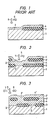
- an insulator film 3 having an opening 2 is formed in the vicinity of the surface of a semiconductor substrate 1
- a polycrystalline or amorphous silicon film 4 is deposited on the whole surface and is thereafter irradiated with a laser beam or electron beam 5
- a laser beam or electron beam 5 Japanese Laid-open Patent Application No. 56-73697, and M. Tamura et al., Jpn. J. Appl. Physics, 19, L23, 1980.
- This method can employ a continuous-wave (CW) laser (or electron beam) or pulse laser.
- CW continuous-wave
- the case of using the CW laser (or electron beam) will be explained as an example.
- the part of the polyerystalline or amorphous film 4 deposited on the opening 2 of the insulator film 3 is irradiated with the laser beam (or electron beam) 5.
- the laser beam or electron beam
- this part of the polycrystalline or amorphous silicon film 4 turns into the single crystal owing to upward epitaxial growth.
- the laser beam (or electron beam) 5 is moved in the direction of an arrow 6 while being scanned substantially perpendicularly to the sheet of drawing. Then, lateral epitaxial growth develops to successively single-crystallize the part of the polycrystalline or amorphous silicon film 4 deposited on the insulator film 3.
- the second disadvantage is the variation of a surface shape developing after the irradiation with the laser beam or electron beam. More specifically, when the laser beam or electron beam is scanningly projected, the Si surface layer is once melted and then solidified due to temperature fall, so that the surface of the polycrystalline or amorphous silicon film becomes uneven.
- the surface becomes more uneven. That is, the uneven parts to appear in the surface become greater with increase in the number of times of the irradiation with the laser beam or electron beam.
- An object of the present invention is to solve the problems in the prior art, and to provide a method of producing a single-crystal film by which a single-crystal semiconductor film having a flat surface of slight unevenness can be formed on an insulator film.
- Another object of the present invention is to provide a method of producing a single-crystal semiconductor film by which a plurality of single-crystal semiconductor films having flat surfaces of slight unevenness can be stacked and formed alternately with insulator films.
- Another object of the present invention is to provide a method of producing a single-crystal semiconductor film by which a structure including a part with a plurality of single-crystal semiconductor films and insulator films stacked alternately can be formed owing to only one single operation of crystallisation.
- the growth of a single crystal is executed by the following two steps.
- the first step is a step in which the stage of forming an insulator film having an opening on a single-crystal silicon substrate and then depositing a polycrystalline or amorphous silicon film on the whole surface of the insulator film is repeated a plurality of times, whereby a multilayer structure with the polycrystalline or amorphous silicon films and the insulator films stacked alternately is formed on the single-crystal silicon substrate.
- Figure 2 shows an example. The sizes of openings 2 and 2' in a first insulator film (lower layer) 3 and a second insulator film (upper layer) 3' are unequal.
- the smaller opening namely, the opening 2 of the first insulator film 3 acts as an opening common to the first and second insulator films 3 and 3'.
- the second step is a step in which, next the first step, a laser beam or electron beam is scanningly irradiated to single-crystallize the polycrystalline or amorphous silicon films.
- the polycrystalline or amorphous silicon films 4 and 4' deposited by the first step are melted and then solidified into the single crystal, first in a region .corresponding to the common opening 2.
- the growth of the single crystal proceeds onto the insulator films 3 and 3' with the scanning of the laser beam or electron beam.
- both the polycrystalline or amorphous silicon films 4 and 4' of the lower and upper layers turn into the single crystal, and the structure with the plurality of single-crystal films and insulator films stacked alternately as seen from Figure 2 is formed.
- Si0 2 films 3, 3' and polycrystalline silicon films 4, 4' were formed near the major surface of a single-crystal silicon substrate 1 by well-known techniques. All the thicknesses of the Si0 2 films 3, 3' and the polycrystalline Si films 4, 4' were 100 nm.
- a laser beam 5 the beam of an Ar laser oscillating at an output of 12 W was converged to a diameter of 20 ⁇ m and was scanningly irradiated at a rate of 20 cm/second.
- the polycrystalline silicon film 4' of the upper layer was crystal-grown about 80 pm from the end of the SiO 2 film 3' onto this Si02film 3'.
- the polycrystalline silicon film 4 of the lower layer was crystallized, but the crystallinity of the crystal was not very good. Moreover, the distance of the lower layer single-crystallized by the crystal growth was about 40 ⁇ m from the end part of the insulator film 3 and was shorter than in the case of the upper layer.
- the polycrystalline silicon films 4, 4' of the upper and lower layers were simultaneously heated. More specifically, the beam of a YAG laser oscillating at an output of 30 W was converged to a diameter of 20 pm and was projected while being scanned in the direction of an arrow 6 at a rate of 20 cm/second. When the structure thus treated was observed with an electron microscope, it was confirmed that both the polycrystalline silicon layers 4, 4' of the upper and lower layers were crystallized over regions of 80 pm extending from the ends of the Si0 2 films 3, 3' onto these Si0 2 films.
- the size of the single-crystal silicon film produced by the present examples was approximately 80 11m extending from the end part of the underlying Si0 2 film onto this Si0 2 film. In order to actually form a semiconductor device, it is favorable that the size is as large as possible.
- the openings and 2' are common in the case of Figure 2, the opening 2' of the upper layer and the opening 2 of the lower layer need not always lie in common positions as seen from Figure 3. However, the existence of the common openings is very preferable in practical use.
- all the thicknesses of the polycrystalline silicon films 4, 4' and SiO 2 films 3, 3' were 100 nm and the widths of the Si0 2 films 3, 3' were not greater than 160 ⁇ m.
- Tha beam of a YAG laser oscillating at an output of 30 W was converged to a diameter of 20 11m, and was irradiated on the structure formed as described above, while being scanned at a rate of 20 cm/second. Thereafter, the crystallinity was assessed by the use of observation with an electron microscope. Then, it was confirmed that both the polycrystalline silicon films 4 and 4' were .entirely single-crystallized.
- a plurality of polycrystalline or amorphous silicon films and a plurality of insulator films having openings are alternately stacked and formed, and a laser beam or electron beam is irradiated from above, whereby the plurality of polycrystalline or amorphous silicon , films are single-crystallized.
- the present invention is not restricted to the scanning of the stacked structure by the laser beam or electron beam. Even when a rectilinear strip heater as known from "Appl. Phys. Lett.” 1982, 158-160, is sequentially moved in the directions of the arrows 6 and 7, the single-crystallization can be attained, and this measure is applicable to the present invention.
- the YAG laser is favorable as described above. With this laser, the best results were obtained.
- the distance over which the polycrystalline or amorphous silicon film can be single-crystallized from the end part of the insulator film onto this insulator film is small, and hence, the use of a CW laser is favorable.
- the electron beam need to be irradiated in vacuum, but it has a long distance of permeation. It is also usable in the present invention.
- the Si0 2 film was used as the insulator film.
- Si 3 N 4 and phosphosilicate glass are equivalent to Si0 2 in the coefficient of absorption of the laser beam and the stopping power of the electron beam, and the films of these substances can be used in the present invention similarly to the Si0 2 film.
- the surface is prevented from becoming uneven at the single-crystallization step owing to the insulator film formed thereon.
- the thickness of the insulator film needs to be great to some extent and should favorably be approximately 20 nm or above.
- the thickness is set at approximately 1 ⁇ m or below.
- the laser beam 5 was irradiated with the polycrystalline silicon film 4' of the upper layer exposed, it is a matter of course that the laser beam 5 may be irradiated in the state in which the surface of the polycrystalline or amorphous silicon film 4' of the upper layer is covered with the insulator film. Thus, the occurrence of the uneven parts of the surface of the upper polycrystalline or amorphous silicon film 4' is effectively prevented.
- the maximum thickness to which the polycrystalline or amorphous silicon film can be single-crystallized by the laser irradiation is approximately 10 ⁇ m.
- the irradiation needs to be of very high intensity in order to single-crystallize the lowermost part of the polycrystalline or amorphous silicon film.
- Such irradiation of high intensity melts the vicinity of the surface of the polycrystalline or amorphous silicon film excessively, resulting in conspicuous deformation.
- the sum of the thicknesses of the plurality of polycrystalline or amorphous silicon films in the present invention should favorably be at most approximately 10 ⁇ m to the end of preventing the excessive melting and deformation of the uppermost layer and reliably single-crystallizing the lowermost layer.
- each film should favorably be at least 100 nm.
- the thickness of each polycrystalline or amorphous silicon film to be single-crystallized is selected from a range of 100 nm to 1 um.
- the maximum thickness of the polycrystalline or amorphous film which can be single-crystallized in the present invention is about 10 ⁇ m as stated before, up to 10 layers of polycrystalline or amorphous silicon films can be single-crystallized, assuming that each of the polycrystalline or amorphous silicon films to be stacked alternately with the insulator films is 1 ⁇ m thick.
- the intensity of the laser beam or electron beam is selected from a range of 10 to 50 W or so.
- the plurality of polycrystalline or amorphous silicon films can be turned into the single crystal by one operation of irradiating them with the energy beam or heating them by means of a strip heater. Moreover, at the melting and solidification of the polycrystalline or amorphous silicon, the surface is effectively prevented from becoming uneven owing to the insulator films.
Landscapes
- Chemical & Material Sciences (AREA)
- Engineering & Computer Science (AREA)
- Crystallography & Structural Chemistry (AREA)
- Materials Engineering (AREA)
- Metallurgy (AREA)
- Organic Chemistry (AREA)
- Recrystallisation Techniques (AREA)
- Liquid Deposition Of Substances Of Which Semiconductor Devices Are Composed (AREA)
- Silicon Compounds (AREA)
- Crystals, And After-Treatments Of Crystals (AREA)
Claims (11)
Applications Claiming Priority (2)
| Application Number | Priority Date | Filing Date | Title |
|---|---|---|---|
| JP57075260A JPS58194799A (ja) | 1982-05-07 | 1982-05-07 | 単結晶シリコンの製造方法 |
| JP75260/82 | 1982-05-07 |
Publications (2)
| Publication Number | Publication Date |
|---|---|
| EP0093981A1 EP0093981A1 (de) | 1983-11-16 |
| EP0093981B1 true EP0093981B1 (de) | 1986-03-26 |
Family
ID=13571067
Family Applications (1)
| Application Number | Title | Priority Date | Filing Date |
|---|---|---|---|
| EP83104231A Expired EP0093981B1 (de) | 1982-05-07 | 1983-04-29 | Verfahren zur Herstellung einer Schicht aus einkristallinem Silizium |
Country Status (6)
| Country | Link |
|---|---|
| US (1) | US4599133A (de) |
| EP (1) | EP0093981B1 (de) |
| JP (1) | JPS58194799A (de) |
| KR (1) | KR900004267B1 (de) |
| CA (1) | CA1221606A (de) |
| DE (1) | DE3362661D1 (de) |
Families Citing this family (20)
| Publication number | Priority date | Publication date | Assignee | Title |
|---|---|---|---|---|
| US5753542A (en) | 1985-08-02 | 1998-05-19 | Semiconductor Energy Laboratory Co., Ltd. | Method for crystallizing semiconductor material without exposing it to air |
| JPH084067B2 (ja) * | 1985-10-07 | 1996-01-17 | 工業技術院長 | 半導体装置の製造方法 |
| DE3741671A1 (de) * | 1987-12-09 | 1989-06-22 | Asea Brown Boveri | Cvd-verfahren zur randpassivierung bei halbleiterbauelementen |
| US5329207A (en) * | 1992-05-13 | 1994-07-12 | Micron Technology, Inc. | Field emission structures produced on macro-grain polysilicon substrates |
| JPH076960A (ja) * | 1993-06-16 | 1995-01-10 | Fuji Electric Co Ltd | 多結晶半導体薄膜の生成方法 |
| JP3778456B2 (ja) | 1995-02-21 | 2006-05-24 | 株式会社半導体エネルギー研究所 | 絶縁ゲイト型薄膜半導体装置の作製方法 |
| US6392810B1 (en) | 1998-10-05 | 2002-05-21 | Semiconductor Energy Laboratory Co., Ltd. | Laser irradiation apparatus, laser irradiation method, beam homogenizer, semiconductor device, and method of manufacturing the semiconductor device |
| US6506635B1 (en) | 1999-02-12 | 2003-01-14 | Semiconductor Energy Laboratory Co., Ltd. | Semiconductor device, and method of forming the same |
| JP4827276B2 (ja) | 1999-07-05 | 2011-11-30 | 株式会社半導体エネルギー研究所 | レーザー照射装置、レーザー照射方法及び半導体装置の作製方法 |
| TW473783B (en) | 1999-08-13 | 2002-01-21 | Semiconductor Energy Lab | Laser apparatus, laser annealing method, and manufacturing method of a semiconductor device |
| US6548370B1 (en) * | 1999-08-18 | 2003-04-15 | Semiconductor Energy Laboratory Co., Ltd. | Method of crystallizing a semiconductor layer by applying laser irradiation that vary in energy to its top and bottom surfaces |
| US7078321B2 (en) | 2000-06-19 | 2006-07-18 | Semiconductor Energy Laboratory Co., Ltd. | Semiconductor device and method of manufacturing the same |
| KR100397762B1 (ko) * | 2000-10-09 | 2003-09-13 | (주)쎄미시스코 | 비정질 실리콘 박막의 결정화 방법 |
| JP4275336B2 (ja) * | 2001-11-16 | 2009-06-10 | 株式会社半導体エネルギー研究所 | 半導体装置の作製方法 |
| US6977775B2 (en) * | 2002-05-17 | 2005-12-20 | Sharp Kabushiki Kaisha | Method and apparatus for crystallizing semiconductor with laser beams |
| US7259082B2 (en) * | 2002-10-03 | 2007-08-21 | Semiconductor Energy Laboratory Co., Ltd. | Method of manufacturing semiconductor device |
| US7405114B2 (en) * | 2002-10-16 | 2008-07-29 | Semiconductor Energy Laboratory Co., Ltd. | Laser irradiation apparatus and method of manufacturing semiconductor device |
| US7335255B2 (en) * | 2002-11-26 | 2008-02-26 | Semiconductor Energy Laboratory, Co., Ltd. | Manufacturing method of semiconductor device |
| US6932865B2 (en) * | 2003-04-11 | 2005-08-23 | Lockheed Martin Corporation | System and method of making single-crystal structures through free-form fabrication techniques |
| US7261779B2 (en) * | 2003-06-05 | 2007-08-28 | Lockheed Martin Corporation | System, method, and apparatus for continuous synthesis of single-walled carbon nanotubes |
Family Cites Families (10)
| Publication number | Priority date | Publication date | Assignee | Title |
|---|---|---|---|---|
| US4046618A (en) * | 1972-12-29 | 1977-09-06 | International Business Machines Corporation | Method for preparing large single crystal thin films |
| FR2292677A1 (fr) * | 1974-11-26 | 1976-06-25 | Aquitaine Petrole | Traitement d'assainissement des effluents de forages petroliers |
| US4059461A (en) * | 1975-12-10 | 1977-11-22 | Massachusetts Institute Of Technology | Method for improving the crystallinity of semiconductor films by laser beam scanning and the products thereof |
| JPS56142630A (en) * | 1980-04-09 | 1981-11-07 | Fujitsu Ltd | Manufacture of semiconductor device |
| US4323417A (en) * | 1980-05-06 | 1982-04-06 | Texas Instruments Incorporated | Method of producing monocrystal on insulator |
| JPS5734331A (en) * | 1980-08-11 | 1982-02-24 | Toshiba Corp | Manufacture of semiconductor device |
| US4330363A (en) * | 1980-08-28 | 1982-05-18 | Xerox Corporation | Thermal gradient control for enhanced laser induced crystallization of predefined semiconductor areas |
| US4358326A (en) * | 1980-11-03 | 1982-11-09 | International Business Machines Corporation | Epitaxially extended polycrystalline structures utilizing a predeposit of amorphous silicon with subsequent annealing |
| JPS57136342A (en) * | 1981-02-17 | 1982-08-23 | Fujitsu Ltd | Manufacture of semiconductor device |
| US4388145A (en) * | 1981-10-29 | 1983-06-14 | Xerox Corporation | Laser annealing for growth of single crystal semiconductor areas |
-
1982
- 1982-05-07 JP JP57075260A patent/JPS58194799A/ja active Pending
-
1983
- 1983-04-29 DE DE8383104231T patent/DE3362661D1/de not_active Expired
- 1983-04-29 EP EP83104231A patent/EP0093981B1/de not_active Expired
- 1983-05-02 KR KR1019830001854A patent/KR900004267B1/ko not_active Expired
- 1983-05-04 US US06/491,544 patent/US4599133A/en not_active Expired - Lifetime
- 1983-05-06 CA CA000427661A patent/CA1221606A/en not_active Expired
Non-Patent Citations (2)
| Title |
|---|
| JAPANESE JOURNAL OF APPLIED PHYSICS, vol. 19, no. 1, January 1980, pages L23-L26 M. TAMURA et al.: "Si bridging epitaxy from Si windows onto Si02 by Q-switched ruby laser pulse annealing" * |
| JAPANESE JOURNAL OF APPLIED PHYSICS, vol. 20, no. 3, March 1981, pages L176-L178 J. SAKURAI et al.: "Lateral epitaxial growth in poly-Si film over Si02 from single-Si seed by scanning CW ar laser annealing" * |
Also Published As
| Publication number | Publication date |
|---|---|
| DE3362661D1 (en) | 1986-04-30 |
| KR900004267B1 (ko) | 1990-06-18 |
| CA1221606A (en) | 1987-05-12 |
| KR840004984A (ko) | 1984-10-31 |
| JPS58194799A (ja) | 1983-11-12 |
| US4599133A (en) | 1986-07-08 |
| EP0093981A1 (de) | 1983-11-16 |
Similar Documents
| Publication | Publication Date | Title |
|---|---|---|
| US4599133A (en) | Method of producing single-crystal silicon film | |
| EP0047140B1 (de) | Verfahren zum Umwandeln von Halbleiterzonen in monokristalline Zonen | |
| EP0127323B1 (de) | Verfahren zum Herstellen einer einkristallinen Halbleiterinsel auf einem Isolator | |
| EP0235819B1 (de) | Verfahren zum Herstellen einer monokristallinen Halbleiterschicht | |
| Biegelsen et al. | Laser‐induced crystallization of silicon islands on amorphous substrates: Multilayer structures | |
| US4596604A (en) | Method of manufacturing a multilayer semiconductor device | |
| CA1203148A (en) | Method of manufacturing single-crystal film | |
| JPH0157078B2 (de) | ||
| EP0236953B1 (de) | Herstellungsverfahren einer Halbleiter-Kristallschicht | |
| US4714684A (en) | Method of forming single crystal layer on dielectric layer by controlled rapid heating | |
| JPH027415A (ja) | Soi薄膜形成方法 | |
| JPS6119116A (ja) | 半導体装置の製造方法 | |
| JP2929660B2 (ja) | 半導体装置の製造方法 | |
| JP2993107B2 (ja) | 半導体薄膜の製造方法 | |
| JPH0442358B2 (de) | ||
| Tamura et al. | Laser-Induced Lateral, Vertically-Seeded Epitaxial Regrowth of Deposited Si Films over Various SiO2 Patterns | |
| JPH024559B2 (de) | ||
| JPS6351370B2 (de) | ||
| JPS60246619A (ja) | 半導体装置の製造方法 | |
| KR940006697B1 (ko) | Soi모스 제조방법 | |
| JPS6038809A (ja) | 半導体装置の製造方法 | |
| JPH0523492B2 (de) | ||
| JPH0691008B2 (ja) | Soi基板の製造方法 | |
| JPH01297814A (ja) | 単結晶薄膜の製造方法 | |
| JPH0693428B2 (ja) | 多層半導体基板の製造方法 |
Legal Events
| Date | Code | Title | Description |
|---|---|---|---|
| PUAI | Public reference made under article 153(3) epc to a published international application that has entered the european phase |
Free format text: ORIGINAL CODE: 0009012 |
|
| AK | Designated contracting states |
Designated state(s): DE FR GB IT NL |
|
| 17P | Request for examination filed |
Effective date: 19831222 |
|
| GRAA | (expected) grant |
Free format text: ORIGINAL CODE: 0009210 |
|
| AK | Designated contracting states |
Kind code of ref document: B1 Designated state(s): DE FR GB IT NL |
|
| REF | Corresponds to: |
Ref document number: 3362661 Country of ref document: DE Date of ref document: 19860430 |
|
| ITF | It: translation for a ep patent filed | ||
| ET | Fr: translation filed | ||
| PLBE | No opposition filed within time limit |
Free format text: ORIGINAL CODE: 0009261 |
|
| STAA | Information on the status of an ep patent application or granted ep patent |
Free format text: STATUS: NO OPPOSITION FILED WITHIN TIME LIMIT |
|
| 26N | No opposition filed | ||
| PG25 | Lapsed in a contracting state [announced via postgrant information from national office to epo] |
Ref country code: GB Effective date: 19880429 |
|
| GBPC | Gb: european patent ceased through non-payment of renewal fee | ||
| PG25 | Lapsed in a contracting state [announced via postgrant information from national office to epo] |
Ref country code: FR Free format text: LAPSE BECAUSE OF NON-PAYMENT OF DUE FEES Effective date: 19881229 |
|
| PG25 | Lapsed in a contracting state [announced via postgrant information from national office to epo] |
Ref country code: DE Effective date: 19890103 |
|
| REG | Reference to a national code |
Ref country code: FR Ref legal event code: ST |
|
| ITTA | It: last paid annual fee | ||
| PGFP | Annual fee paid to national office [announced via postgrant information from national office to epo] |
Ref country code: NL Payment date: 19930430 Year of fee payment: 11 |
|
| PG25 | Lapsed in a contracting state [announced via postgrant information from national office to epo] |
Ref country code: NL Effective date: 19941101 |
|
| NLV4 | Nl: lapsed or anulled due to non-payment of the annual fee |