EP0094426B1 - Kontrolle des bandabstandes in amorphen halbleitern - Google Patents
Kontrolle des bandabstandes in amorphen halbleitern Download PDFInfo
- Publication number
- EP0094426B1 EP0094426B1 EP83900227A EP83900227A EP0094426B1 EP 0094426 B1 EP0094426 B1 EP 0094426B1 EP 83900227 A EP83900227 A EP 83900227A EP 83900227 A EP83900227 A EP 83900227A EP 0094426 B1 EP0094426 B1 EP 0094426B1
- Authority
- EP
- European Patent Office
- Prior art keywords
- temperature
- substrate
- reactor
- bandgap
- reaction
- Prior art date
- Legal status (The legal status is an assumption and is not a legal conclusion. Google has not performed a legal analysis and makes no representation as to the accuracy of the status listed.)
- Expired
Links
Images


Classifications
-
- H—ELECTRICITY
- H10—SEMICONDUCTOR DEVICES; ELECTRIC SOLID-STATE DEVICES NOT OTHERWISE PROVIDED FOR
- H10D—INORGANIC ELECTRIC SEMICONDUCTOR DEVICES
- H10D62/00—Semiconductor bodies, or regions thereof, of devices having potential barriers
- H10D62/40—Crystalline structures
- H10D62/402—Amorphous materials
-
- H—ELECTRICITY
- H10—SEMICONDUCTOR DEVICES; ELECTRIC SOLID-STATE DEVICES NOT OTHERWISE PROVIDED FOR
- H10P—GENERIC PROCESSES OR APPARATUS FOR THE MANUFACTURE OR TREATMENT OF DEVICES COVERED BY CLASS H10
- H10P14/00—Formation of materials, e.g. in the shape of layers or pillars
- H10P14/20—Formation of materials, e.g. in the shape of layers or pillars of semiconductor materials
- H10P14/24—Formation of materials, e.g. in the shape of layers or pillars of semiconductor materials using chemical vapour deposition [CVD]
-
- H—ELECTRICITY
- H10—SEMICONDUCTOR DEVICES; ELECTRIC SOLID-STATE DEVICES NOT OTHERWISE PROVIDED FOR
- H10P—GENERIC PROCESSES OR APPARATUS FOR THE MANUFACTURE OR TREATMENT OF DEVICES COVERED BY CLASS H10
- H10P14/00—Formation of materials, e.g. in the shape of layers or pillars
- H10P14/20—Formation of materials, e.g. in the shape of layers or pillars of semiconductor materials
- H10P14/29—Formation of materials, e.g. in the shape of layers or pillars of semiconductor materials characterised by the substrates
- H10P14/2901—Materials
- H10P14/2902—Materials being Group IVA materials
- H10P14/2905—Silicon, silicon germanium or germanium
-
- H—ELECTRICITY
- H10—SEMICONDUCTOR DEVICES; ELECTRIC SOLID-STATE DEVICES NOT OTHERWISE PROVIDED FOR
- H10P—GENERIC PROCESSES OR APPARATUS FOR THE MANUFACTURE OR TREATMENT OF DEVICES COVERED BY CLASS H10
- H10P14/00—Formation of materials, e.g. in the shape of layers or pillars
- H10P14/20—Formation of materials, e.g. in the shape of layers or pillars of semiconductor materials
- H10P14/34—Deposited materials, e.g. layers
- H10P14/3402—Deposited materials, e.g. layers characterised by the chemical composition
- H10P14/3404—Deposited materials, e.g. layers characterised by the chemical composition being Group IVA materials
- H10P14/3411—Silicon, silicon germanium or germanium
-
- H—ELECTRICITY
- H10—SEMICONDUCTOR DEVICES; ELECTRIC SOLID-STATE DEVICES NOT OTHERWISE PROVIDED FOR
- H10P—GENERIC PROCESSES OR APPARATUS FOR THE MANUFACTURE OR TREATMENT OF DEVICES COVERED BY CLASS H10
- H10P14/00—Formation of materials, e.g. in the shape of layers or pillars
- H10P14/20—Formation of materials, e.g. in the shape of layers or pillars of semiconductor materials
- H10P14/34—Deposited materials, e.g. layers
- H10P14/3438—Doping during depositing
- H10P14/3441—Conductivity type
- H10P14/3442—N-type
-
- H—ELECTRICITY
- H10—SEMICONDUCTOR DEVICES; ELECTRIC SOLID-STATE DEVICES NOT OTHERWISE PROVIDED FOR
- H10P—GENERIC PROCESSES OR APPARATUS FOR THE MANUFACTURE OR TREATMENT OF DEVICES COVERED BY CLASS H10
- H10P14/00—Formation of materials, e.g. in the shape of layers or pillars
- H10P14/20—Formation of materials, e.g. in the shape of layers or pillars of semiconductor materials
- H10P14/34—Deposited materials, e.g. layers
- H10P14/3438—Doping during depositing
- H10P14/3441—Conductivity type
- H10P14/3444—P-type
Definitions
- the invention relates to a method of production of amorphous semiconductors with a specified bandgap wherein at least one higher order semiconductane contained in a gaseous phase mixture (G) is introduced in a reaction chamber wherein a substrate is provided, said substrate being subjected to controlled heating.
- G gaseous phase mixture
- Semiconductors have an extended region of discontinuity in their internal energy levels between their valence and conduction bands. This region of discontinuity is known as a "bandgap". It determines how a device made from the material will respond to external stimuli.
- the invention as claimed is intended to remedy this drawback. It solves the problem of how to achieve the production of hydrogenated amorphous silicon with a specified bandgap at comparatively low temperatures.
- the invention provides a method of preparing an amorphous semiconductor with a specified bandgap by the pyrolytic decomposition of one or more gaseous phase polysemiconducta- nes at a specified temperature for each desired bandgap.
- the pyrolytic decomposition forms a deposit over a reaction range of temperature between 300°C and 500°C within the total range of temperature over which the deposition can take place.
- the deposition takes place in a reactor which is maintained at a different temperature than the average temperature of the deposit that is formed.
- the deposit is desirably made on a substrate within the reactor, and the deposition temperature is substantially that of the substrate.
- the temperature of the reactor is maintained at a different level than the temperature of the substrate.
- the reactor may be maintained at a temperature which is greater than or less than that of the reaction, with a difference in the two temperatures being maintained over the time of the reaction.
- the reaction desirably takes place in the temperature range between about 300°C and 475°C.
- the reaction temperature can be permitted to vary within a prescribed range, which can vary between about 5 percent above and about 5 percent below the average temperature of the reaction.
- the semiconductanes which are pyrolytically decomposed can be diluted with an inert gas, such as argon, helium, neon, xenon, or hydrogen.
- the semiconductanes are desirably selected from the class of silanes, germanes and mixtures of the two.
- the gas from which the deposit takes place can be in the form of a stream which flows continuously into and out of the reactor.
- the gas may be made to directly impinge on a heated substrate by, for example, the use of a directive nozzle.
- the gas may be static within the reactor.
- the gaseous medium from which the deposit takes place may include a suitable dopant.
- suitable dopants are the trihydrides or trihalides of phosphorus, arsenic and tin, as well as diborane.
- Organometallic compounds of elements such as aluminium and gallium may also be employed.
- FIGURE 1 a flow chart 100 for the general practice of the invention is set forth in FIGURE 1.
- the process begins with the introduction of a gaseous phase mixture containing at least one higher order silane into a reaction chamber, as illustrated in block 101.
- the gaseous phase mixture has its desired temperature and/or pressure controlled in accordance with block 102.
- the result, as indicated in block 103, is the pyrolytic decomposition of the gaseous phase mixture to deposit amorphous silicon having a specified bandgap.
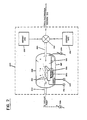
- FIGURE 2 An illustrative arrangement 250 for producing semiconductors with controlled bandgaps is illustrated in FIGURE 2.
- the semiconductanes to be converted including higher order silanes, are prepared in a preliminary section 210 (not shown) and introduced at a mixing valve 251.
- the latter permits the controlled introduction either simultaneously or at desired intervals of time, of dopant gases from source 252 and/or 255.
- the result is a gaseous stream which is applied at an inlet 263 of a reaction chamber 260.
- the incoming gaseous stream, indicated by the arrow G, is drawn over the substrate 262 by the action of a vacuum pump 280.
- the substrate 262 is subjected to controlled heating by a heater 266r in a holder 266.
- a current is applied to the heater 266r from an adjustable source 290.
- the temperature of the substrate is monitored by a gauge 291 which illustratively extends to the substrate 262.
- a further gauge 264 for the vacuum pump 280 gives an indication of the pressure within the reaction chamber 260.
- the incoming gaseous phase mixture G As the incoming gaseous phase mixture G is drawn over the heated substrate 262 it pyrolytically decomposes and forms an amorphous semiconductor on the upper surface of the substrate, as indicated by the dashed line arrows D.
- the portion of the gaseous phase mixture that does not participate in the pyrolytic decomposition is drawn from the chamber into the vacuum pump 280 as exhaust gas E.
- the semiconductor material that becomes pyrolytically deposited on the substrate has a prescribed bandgap.
- the bandgap of the deposited material changes accordingly.
- the control that is achieved in accordance with the invention over the bandgap appears to result from the changes that are controllably made in the amount of hydrogen bonded to the semiconductane atoms of the deposit. While it has been known that many amorphous semiconductors, such as those produced by gaseous discharge, have hydrogen compensated defects because of ion bombardment, it has been believed that amorphous films produced by pyrolytic decomposition contained little hydrogen bonding. It was further believed that at low pressure levels where there was virtually no ion bombardment in the pyrolytic process, there was no hydrogen bonding in the resulting amorphous silicon.
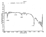
- FIGURE 3 is a computer print in which the computer was programmed to note any significant absorptions.
- FIGURE 3 shows significant absorptions at 2355, 1682 and 1104 wave numbers, in addition to the significant silicon hydride absorption at 1978 wave numbers.
- One measure of the improved performance of materials with controlled bandgaps in accordance with the invention is that as temperature is increased we have been able to measure both a reduction in bandgap and an increase in short- circuit current. We have speculated that this results because an increase in temperature leads to greater coherence and ordering in the semiconductor structure, requiring a reduced amount of hydrogen for defect compensation. This is opposite to what has been observed for amorphous silicon produced in other ways, such as glow discharge, in which the excessive defect condition caused by ion bombardment appears to prevent the material from achieving greater coherence as temperature is increased.
- FIGURE 4 An illustrative reaction chamber 100 for producing semiconductors with controlled bandgaps is illustrated in FIGURE 4.
- the reaction chamber 100 is used in a process that begins with the introduction of a gaseous medium containing at least one higher order semiconductane.
- the gaseous medium is controlled in temperature and/or pressure to being about a pyrolytic deposit of semiconductive material having a specified bandgap.
- the reactor 100 is of the hot-wall epitaxial type, i.e., the decomposition of gases takes place at the wall of the reactor, and a deposit is formed on the substrate 130.
- the wall or closure 110 of the reactor 100 typically of quartz, is surrounded over its principal cylindrical body portion by a heating coil 120. The latter is used to apply heat directly to the wall 110 and maintain it at a prescribed temperature level. This is by contrast with the similar reactor 250 shown in FIGURE 2.
- the heating effect from the coil 120 is radiated from the wall 110 onto the substrate 130.
- the substrate may have an additional heating effect produced by an internal heating coil 132, or a cooling effect by an internal coolant pipe, which is substituted for the coil 132.
- thermocouple 111 The temperature of the wall is monitored by a thermocouple 111, while the temperature of the substrate is monitored by a thermocouple 131.
- Semiconductanes that are to be pyrolytically decomposed in accordance with the invention are introduced into the reactor 100 at an inlet 140 through an appropriate mixing valve 150.
- the gaseous medium is exhausted through a vacuum pump 160 through an outlet valve 170.
- Pressure within the chamber 100 is monitored by a gauge 180.
- the pyrolytic deposit formed on the substrate 130 may be produced by either static or dynamic action of the gaseous medium.
- static deposition the semiconductanes are introduced into the evacuated reactor 100 through the valve 150.
- the exhaust valve 170 and the inlet valve 150 are then shut, causing a specified volume of gaseous medium to be trapped in the chamber 100.
- the trapped gas decomposed on both the wall 110 and the substrate 130.
- the result is a desired amorphous silicon hydride film having a specified bandgap.
- the static system has the advantage of economizing on the volume and pumping of the gaseous medium.
- the gaseous medium flows continuously through the chamber 100 at a desired rate determined by the settings of the inlet valve 150 and the exhaust valve 170.
- a new reaction mixture is continuously introduced into the chamber 100 and all components of the gaseous medium maintain their relative partial pressures.
- the dynamic arrangement however, has the disadvantage of some waste of the gaseous medium since a considerable amount of the gas is exhausted through the vacuum pump 160 without decomposing to form the semiconductor deposit.
- An illustrative gaseous medium has the mass-spectrometer plot of FIGURE 5.
- the medium is a mixture of monosilanes, disilanes and trisilanes.
- the monosilanes are indicated by peaks between mass numbers 28 and 34.
- the disilanes are indicated by peaks between mass numbers 56 and 64, while the trisilanes have peaks between mass numbers 84 and 93.
- the mass-spectrometer plot of FIGURE 5 also indicates the absence of moisture and hydrogen chloride. For example, if moisture were present, it would be indicated by peaks in the vicinity of mass number 18. As is apparent, there is no indication at that particular mass number position. Since disilanes, e.g.
- the mixture of FIGURE 5 results from the preparation of the higher order silanes under conditions which limit the creation of impurities or result from trapping of the impurities in standard cold traps.
- the curve T 1 for a temperature of 375°C., the curve T 2 for a temperature of 425°C., and the curve T 3 for a temperature of 450°C. all have essentially the same slope measured in terms of the ration of the change in the square root of the absorption coefficient times energy to the change in energy. This is significantly different from experience with glow discharge and other materials in which a significant decrease in energy gap is accompanied by a shallower slope and hence a reduced photovoltaic effect.
- the distinct variations in energy gap for the different temperatures of pyrolytic decomposition is attributed to the different concentrations of hydrogen that result in the deposits.
- the test results indicate that the controlling factor in determining the bandgap of the deposited material is that the substrate temperature be the same whether the reaction chamber is of the cold-wall or the hot-wall type.
- the substrate temperature should be maintained within ten degrees above and below the nominal value of the desired bandgap.
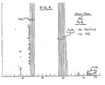
- FIGURE 8 An infra-red spectrum of an amorphous silicon hydride film deposited in the reactor of FIGURE 4 on a crystalline silicon substrate is shown in FIGURE 8.
- the spectrum has a characteristic silicon hydride stretch bond at 1980 wave num- bers/reciprocal centimeters. It is to be noted that other absorption bands centered at 1170 and 750 wave numbers are attributable to suitable oxide bonding in the crystalline silicon substrate and consequently play no role in the silicon hydride that produces bandgap control according to the invention.
- FIGURE 8 also shows a minor absorption peak at 870 wave numbers. This is likely to be substrate absorption. In any event, even if it could be associated with silicon-dihydrogen bonding, its effect would be too insignificant to adversely influence the silicon hydride that is formed.
- a mixture of semiconductanes including monosilanes, disilanes and trisilanes was prepared.
- the body of the reaction chamber was maintained at a fixed temperature above that of the substrate.
- An epitaxial film of amorphous silicon was deposited on the substrate and found to have a bandgap in the range from about 1.58 to about 1.60 electron volts.
- Example I was repeated except that the reaction chamber was maintained at a relatively constant temperature below that of the substrate. The result was substantially the same as the result for Example 1.
- Example I was repeated except that the reaction chamber was unheated, and was of the cold-wall type. The results were the same as for Example I.
- Example I The preceding examples were repeated except that the substrate temperature was permitted to vary in the range from about 2 percent above and 2 percent below the reaction temperature. The result was substantially the same as for Example I.
- the foregoing examples were repeated except that the substrate temperature was increased to about 475°C and held at substantially that level during pyrolytic decomposition.
- the resulting amorphous silicon deposit was found to have a reduced bandgap in the range from about 1.48 to about 1.50 electron volts.
- disilane is known to decompose into silane and silane-dihydride, so that the presence of independent silanes merely supplements the silanes that are produced by the decomposition of higher order silanes, and may slow the reaction down somewhat.
- Example V it has been noted that the addition of inert gases such as argon only affect the growth rate of the pyrolytically produced films. This comes about because there is a reduction in the partial pressure of the higher order silanes for a given total pressure.
- Other inert gases such as helium, nenon, xenon and hydrogen have a similar effect.
- FIGURES 9 and 10 compare the conductivities of n-type doped and undoped films as a function of temperature.
- doped film was prepared using phosphine and the gaseous medium had the approximate composition of FIGURE 5, including monosilanes.
- the conductivity of an undoped film is comparatively low and the activation energy is comparatively high, indicating that the material is intrinsic or undoped. It has a Fermi level of approximately 0.61 electron volts below the conduction band and is in fact the middle of the bandgap.
- Suitable dopants include stibine, arsine and phosphorus trichloride for producing n-type material, and diborane, together with organometallic compounds of aluminum and gallium for producing p-type material.
Landscapes
- Chemical Vapour Deposition (AREA)
- Photovoltaic Devices (AREA)
- Bipolar Transistors (AREA)
- Electroluminescent Light Sources (AREA)
- Liquid Deposition Of Substances Of Which Semiconductor Devices Are Composed (AREA)
- Light Receiving Elements (AREA)
Claims (11)
Priority Applications (1)
| Application Number | Priority Date | Filing Date | Title |
|---|---|---|---|
| AT83900227T ATE28768T1 (de) | 1981-11-20 | 1982-11-19 | Kontrolle des bandabstandes in amorphen halbleitern. |
Applications Claiming Priority (4)
| Application Number | Priority Date | Filing Date | Title |
|---|---|---|---|
| US323585 | 1981-11-20 | ||
| US06/323,585 US4465706A (en) | 1981-11-20 | 1981-11-20 | Bandgap control in amorphous semiconductors |
| US06/337,627 US4485128A (en) | 1981-11-20 | 1982-01-07 | Bandgap control in amorphous semiconductors |
| US337627 | 1982-01-07 |
Publications (3)
| Publication Number | Publication Date |
|---|---|
| EP0094426A1 EP0094426A1 (de) | 1983-11-23 |
| EP0094426A4 EP0094426A4 (de) | 1984-07-18 |
| EP0094426B1 true EP0094426B1 (de) | 1987-08-05 |
Family
ID=26984040
Family Applications (1)
| Application Number | Title | Priority Date | Filing Date |
|---|---|---|---|
| EP83900227A Expired EP0094426B1 (de) | 1981-11-20 | 1982-11-19 | Kontrolle des bandabstandes in amorphen halbleitern |
Country Status (6)
| Country | Link |
|---|---|
| EP (1) | EP0094426B1 (de) |
| JP (1) | JPS58501975A (de) |
| AT (1) | ATE28768T1 (de) |
| AU (1) | AU1100582A (de) |
| DE (1) | DE3276918D1 (de) |
| WO (1) | WO1983001865A1 (de) |
Families Citing this family (3)
| Publication number | Priority date | Publication date | Assignee | Title |
|---|---|---|---|---|
| GB2177119B (en) * | 1985-06-26 | 1989-04-26 | Plessey Co Plc | Organometallic chemical vapour deposition |
| US5155567A (en) * | 1990-01-17 | 1992-10-13 | Ricoh Company, Ltd. | Amorphous photoconductive material and photosensor employing the photoconductive material |
| JP3099957B2 (ja) * | 1990-01-17 | 2000-10-16 | 株式会社リコー | 光導電部材 |
Family Cites Families (6)
| Publication number | Priority date | Publication date | Assignee | Title |
|---|---|---|---|---|
| US4237150A (en) * | 1979-04-18 | 1980-12-02 | The United States Of America As Represented By The United States Department Of Energy | Method of producing hydrogenated amorphous silicon film |
| US4237151A (en) * | 1979-06-26 | 1980-12-02 | The United States Of America As Represented By The United States Department Of Energy | Thermal decomposition of silane to form hydrogenated amorphous Si film |
| US4363828A (en) * | 1979-12-12 | 1982-12-14 | International Business Machines Corp. | Method for depositing silicon films and related materials by a glow discharge in a disiland or higher order silane gas |
| NL8104140A (nl) * | 1980-09-09 | 1982-04-01 | Energy Conversion Devices Inc | Werkwijze voor het vervaardigen van amorfe halfgeleiderinrichtingen met verbeterde fotogevoelige eigenschappen alsmede als zodanig verkregen inrichtingen. |
| US4357179A (en) * | 1980-12-23 | 1982-11-02 | Bell Telephone Laboratories, Incorporated | Method for producing devices comprising high density amorphous silicon or germanium layers by low pressure CVD technique |
| US4339470A (en) * | 1981-02-13 | 1982-07-13 | Rca Corporation | Fabricating amorphous silicon solar cells by varying the temperature _of the substrate during deposition of the amorphous silicon layer |
-
1982
- 1982-11-19 WO PCT/US1982/001640 patent/WO1983001865A1/en not_active Ceased
- 1982-11-19 AU AU1100582A patent/AU1100582A/ active Pending
- 1982-11-19 EP EP83900227A patent/EP0094426B1/de not_active Expired
- 1982-11-19 AT AT83900227T patent/ATE28768T1/de not_active IP Right Cessation
- 1982-11-19 JP JP83500246A patent/JPS58501975A/ja active Pending
- 1982-11-19 DE DE8383900227T patent/DE3276918D1/de not_active Expired
Non-Patent Citations (1)
| Title |
|---|
| Journal De Physique, Colloque Ce, supplement au no. 10, Tome 42, issued October 1981 * |
Also Published As
| Publication number | Publication date |
|---|---|
| EP0094426A4 (de) | 1984-07-18 |
| WO1983001865A1 (en) | 1983-05-26 |
| ATE28768T1 (de) | 1987-08-15 |
| AU1100582A (en) | 1983-06-01 |
| EP0094426A1 (de) | 1983-11-23 |
| JPS58501975A (ja) | 1983-11-17 |
| DE3276918D1 (en) | 1987-09-10 |
Similar Documents
| Publication | Publication Date | Title |
|---|---|---|
| US4485128A (en) | Bandgap control in amorphous semiconductors | |
| US4237150A (en) | Method of producing hydrogenated amorphous silicon film | |
| US4993357A (en) | Apparatus for atomic layer epitaxial growth | |
| US3979271A (en) | Deposition of solid semiconductor compositions and novel semiconductor materials | |
| EP0062079B1 (de) | Dünner silikonfilm und verfahren zu dessen herstellung | |
| CA2095449C (en) | Supersaturated rare earth doped semiconductor layers by chemical vapor deposition | |
| EP0040939B1 (de) | Herstellung von Cadmium-Quecksilber-Telluriden | |
| US4237151A (en) | Thermal decomposition of silane to form hydrogenated amorphous Si film | |
| EP0476676B1 (de) | Verfahren zur Abscheidung eines dünnen Films | |
| DE69702620T2 (de) | Verfahren zur Epitaxiezüchtung | |
| US5397737A (en) | Deposition of device quality low H content, amorphous silicon films | |
| EP0069580B1 (de) | Verfahren zur Herstellung von dünnen Schichten aus Silizium | |
| Houng et al. | Te doping of GaAs and AlxGa1− xAs using diethyltellurium in low pressure OMVPE | |
| US4908074A (en) | Gallium arsenide on sapphire heterostructure | |
| US3208888A (en) | Process of producing an electronic semiconductor device | |
| US5776819A (en) | Deposition of device quality, low hydrogen content, amorphous silicon films by hot filament technique using "safe" silicon source gas | |
| US6334901B1 (en) | Apparatus for forming semiconductor crystal | |
| EP0094426B1 (de) | Kontrolle des bandabstandes in amorphen halbleitern | |
| US3765960A (en) | Method for minimizing autodoping in epitaxial deposition | |
| US4755483A (en) | Method for producing semiconductor device with p-type amorphous silicon carbide semiconductor film formed by photo-chemical vapor deposition | |
| US6124186A (en) | Deposition of device quality, low hydrogen content, hydrogenated amorphous silicon at high deposition rates with increased stability using the hot wire filament technique | |
| Todd et al. | Growth of heteroepitaxial Si1− x− y Ge x C y alloys on silicon using novel deposition chemistry | |
| US4478654A (en) | Amorphous silicon carbide method | |
| JP3214505B2 (ja) | 半導体装置の製造方法 | |
| US4465706A (en) | Bandgap control in amorphous semiconductors |
Legal Events
| Date | Code | Title | Description |
|---|---|---|---|
| PUAI | Public reference made under article 153(3) epc to a published international application that has entered the european phase |
Free format text: ORIGINAL CODE: 0009012 |
|
| AK | Designated contracting states |
Designated state(s): AT BE CH DE FR GB LI LU NL SE |
|
| 17P | Request for examination filed |
Effective date: 19830927 |
|
| GRAA | (expected) grant |
Free format text: ORIGINAL CODE: 0009210 |
|
| AK | Designated contracting states |
Kind code of ref document: B1 Designated state(s): AT BE CH DE FR GB LI LU NL SE |
|
| PG25 | Lapsed in a contracting state [announced via postgrant information from national office to epo] |
Ref country code: NL Effective date: 19870805 Ref country code: AT Effective date: 19870805 |
|
| REF | Corresponds to: |
Ref document number: 28768 Country of ref document: AT Date of ref document: 19870815 Kind code of ref document: T |
|
| PG25 | Lapsed in a contracting state [announced via postgrant information from national office to epo] |
Ref country code: SE Effective date: 19870831 |
|
| REF | Corresponds to: |
Ref document number: 3276918 Country of ref document: DE Date of ref document: 19870910 |
|
| PG25 | Lapsed in a contracting state [announced via postgrant information from national office to epo] |
Ref country code: LU Free format text: LAPSE BECAUSE OF NON-PAYMENT OF DUE FEES Effective date: 19871130 |
|
| ET | Fr: translation filed | ||
| NLV1 | Nl: lapsed or annulled due to failure to fulfill the requirements of art. 29p and 29m of the patents act | ||
| PLBE | No opposition filed within time limit |
Free format text: ORIGINAL CODE: 0009261 |
|
| STAA | Information on the status of an ep patent application or granted ep patent |
Free format text: STATUS: NO OPPOSITION FILED WITHIN TIME LIMIT |
|
| 26N | No opposition filed | ||
| PG25 | Lapsed in a contracting state [announced via postgrant information from national office to epo] |
Ref country code: GB Effective date: 19881119 |
|
| PG25 | Lapsed in a contracting state [announced via postgrant information from national office to epo] |
Ref country code: LI Effective date: 19881130 Ref country code: CH Effective date: 19881130 Ref country code: BE Effective date: 19881130 |
|
| BERE | Be: lapsed |
Owner name: CHRONAR CORP. Effective date: 19881130 |
|
| GBPC | Gb: european patent ceased through non-payment of renewal fee | ||
| PG25 | Lapsed in a contracting state [announced via postgrant information from national office to epo] |
Ref country code: FR Free format text: LAPSE BECAUSE OF NON-PAYMENT OF DUE FEES Effective date: 19890731 |
|
| REG | Reference to a national code |
Ref country code: CH Ref legal event code: PL |
|
| PG25 | Lapsed in a contracting state [announced via postgrant information from national office to epo] |
Ref country code: DE Effective date: 19890801 |
|
| REG | Reference to a national code |
Ref country code: FR Ref legal event code: ST |