EP0094497A1 - Appareil de détection de courants gazeux - Google Patents
Appareil de détection de courants gazeux Download PDFInfo
- Publication number
- EP0094497A1 EP0094497A1 EP83103015A EP83103015A EP0094497A1 EP 0094497 A1 EP0094497 A1 EP 0094497A1 EP 83103015 A EP83103015 A EP 83103015A EP 83103015 A EP83103015 A EP 83103015A EP 0094497 A1 EP0094497 A1 EP 0094497A1
- Authority
- EP
- European Patent Office
- Prior art keywords
- filter
- flow
- cross
- sectional area
- sensing portion
- Prior art date
- Legal status (The legal status is an assumption and is not a legal conclusion. Google has not performed a legal analysis and makes no representation as to the accuracy of the status listed.)
- Withdrawn
Links
- 238000011144 upstream manufacturing Methods 0.000 claims abstract description 7
- 239000004065 semiconductor Substances 0.000 claims description 22
- 238000002955 isolation Methods 0.000 claims description 6
- 230000007704 transition Effects 0.000 claims 1
- 230000002708 enhancing effect Effects 0.000 abstract 1
- 229910000889 permalloy Inorganic materials 0.000 description 15
- 229910052581 Si3N4 Inorganic materials 0.000 description 8
- 238000005259 measurement Methods 0.000 description 8
- HQVNEWCFYHHQES-UHFFFAOYSA-N silicon nitride Chemical compound N12[Si]34N5[Si]62N3[Si]51N64 HQVNEWCFYHHQES-UHFFFAOYSA-N 0.000 description 8
- 230000008901 benefit Effects 0.000 description 7
- 239000002245 particle Substances 0.000 description 6
- XUIMIQQOPSSXEZ-UHFFFAOYSA-N Silicon Chemical compound [Si] XUIMIQQOPSSXEZ-UHFFFAOYSA-N 0.000 description 5
- 229910052710 silicon Inorganic materials 0.000 description 5
- 239000010703 silicon Substances 0.000 description 5
- PXHVJJICTQNCMI-UHFFFAOYSA-N Nickel Chemical compound [Ni] PXHVJJICTQNCMI-UHFFFAOYSA-N 0.000 description 4
- 230000008859 change Effects 0.000 description 4
- KFZMGEQAYNKOFK-UHFFFAOYSA-N Isopropanol Chemical compound CC(C)O KFZMGEQAYNKOFK-UHFFFAOYSA-N 0.000 description 3
- 238000001514 detection method Methods 0.000 description 3
- 230000000694 effects Effects 0.000 description 3
- 230000007613 environmental effect Effects 0.000 description 3
- 238000000034 method Methods 0.000 description 3
- 230000035945 sensitivity Effects 0.000 description 3
- 239000007787 solid Substances 0.000 description 3
- 238000004544 sputter deposition Methods 0.000 description 3
- XEEYBQQBJWHFJM-UHFFFAOYSA-N Iron Chemical compound [Fe] XEEYBQQBJWHFJM-UHFFFAOYSA-N 0.000 description 2
- 230000002457 bidirectional effect Effects 0.000 description 2
- 230000005484 gravity Effects 0.000 description 2
- 229910052759 nickel Inorganic materials 0.000 description 2
- 230000001681 protective effect Effects 0.000 description 2
- 230000009467 reduction Effects 0.000 description 2
- 230000035939 shock Effects 0.000 description 2
- 230000003321 amplification Effects 0.000 description 1
- 239000013078 crystal Substances 0.000 description 1
- 239000003989 dielectric material Substances 0.000 description 1
- 239000000428 dust Substances 0.000 description 1
- 239000003623 enhancer Substances 0.000 description 1
- 238000005530 etching Methods 0.000 description 1
- 230000002349 favourable effect Effects 0.000 description 1
- 238000010438 heat treatment Methods 0.000 description 1
- 230000003116 impacting effect Effects 0.000 description 1
- 230000001771 impaired effect Effects 0.000 description 1
- 229910052742 iron Inorganic materials 0.000 description 1
- 238000004519 manufacturing process Methods 0.000 description 1
- 239000000463 material Substances 0.000 description 1
- 150000004767 nitrides Chemical class 0.000 description 1
- 238000003199 nucleic acid amplification method Methods 0.000 description 1
- 238000007254 oxidation reaction Methods 0.000 description 1
- 238000002161 passivation Methods 0.000 description 1
- 229920002120 photoresistant polymer Polymers 0.000 description 1
- 230000008569 process Effects 0.000 description 1
- 239000000758 substrate Substances 0.000 description 1
Images

Classifications
-
- G—PHYSICS
- G01—MEASURING; TESTING
- G01F—MEASURING VOLUME, VOLUME FLOW, MASS FLOW OR LIQUID LEVEL; METERING BY VOLUME
- G01F15/00—Details of, or accessories for, apparatus of groups G01F1/00 - G01F13/00 insofar as such details or appliances are not adapted to particular types of such apparatus
- G01F15/12—Cleaning arrangements; Filters
-
- G—PHYSICS
- G01—MEASURING; TESTING
- G01F—MEASURING VOLUME, VOLUME FLOW, MASS FLOW OR LIQUID LEVEL; METERING BY VOLUME
- G01F1/00—Measuring the volume flow or mass flow of fluid or fluent solid material wherein the fluid passes through a meter in a continuous flow
- G01F1/68—Measuring the volume flow or mass flow of fluid or fluent solid material wherein the fluid passes through a meter in a continuous flow by using thermal effects
- G01F1/684—Structural arrangements; Mounting of elements, e.g. in relation to fluid flow
- G01F1/6842—Structural arrangements; Mounting of elements, e.g. in relation to fluid flow with means for influencing the fluid flow
-
- G—PHYSICS
- G01—MEASURING; TESTING
- G01F—MEASURING VOLUME, VOLUME FLOW, MASS FLOW OR LIQUID LEVEL; METERING BY VOLUME
- G01F1/00—Measuring the volume flow or mass flow of fluid or fluent solid material wherein the fluid passes through a meter in a continuous flow
- G01F1/68—Measuring the volume flow or mass flow of fluid or fluent solid material wherein the fluid passes through a meter in a continuous flow by using thermal effects
- G01F1/684—Structural arrangements; Mounting of elements, e.g. in relation to fluid flow
- G01F1/6845—Micromachined devices
-
- G—PHYSICS
- G01—MEASURING; TESTING
- G01F—MEASURING VOLUME, VOLUME FLOW, MASS FLOW OR LIQUID LEVEL; METERING BY VOLUME
- G01F1/00—Measuring the volume flow or mass flow of fluid or fluent solid material wherein the fluid passes through a meter in a continuous flow
- G01F1/68—Measuring the volume flow or mass flow of fluid or fluent solid material wherein the fluid passes through a meter in a continuous flow by using thermal effects
- G01F1/696—Circuits therefor, e.g. constant-current flow meters
Definitions
- Prior EP-A 76 935 (application no. 82 108 570.1) describes a highly sensitive air flow sensor. In some applications this type of air flow sensor and similar sensors like hot wire anemometer need a protective filter device to remove particles, lint and the like that could clog the sensing structure. It is the main object of the present invention to improve the operation and stability of gas flow sensors and in particular of low velocity flow sensors. This object is solved by the invention as characterized in claim 1.
- the invention provides a flow channel having a filter section at its inlet and a sensing section downstream of the filter- section whereat the cross-sectional area of the sensing section is smaller than the cross-sectional area of the filter section, so that the flow velocity inside the sensing section is enhanced with respect to the upstream filter section.
- FIGs 2 to 6 of the drawings correspond to figures 1 to 5 of the above mentioned prior EP-A and figure 7 corresponds to its figure 11.
- the present invention provides both a low flow impedance filter and a flow velocity enhancer.
- the structure shown comprises a tube or housing 100 with low flow impedance filters 102 mounted on each end of housing 100.
- the housing shown contains one or more tapered flow sections 104 which lead to tubes or housing portions 106 having a substantially smaller cross-sectional area than the portion of housing 100 occupied by filters 102. Housing portions 106 direct air flow onto air flow sensor 108, schematically represented as a chip mounted on a header 110 which is mounted on a fixture 112 through which electrical leads 114 are passed.
- air flow sensor 108 schematically represented as a chip mounted on a header 110 which is mounted on a fixture 112 through which electrical leads 114 are passed.
- the present invention is shown as a bidirectional device having a filter 102 and tapered housing sections 104 on each side of housing portions 106.
- a device having only a single filter 102 and a single tapered section to receive air flow from a single direction is also within the scope of'the present invention.
- the present invention is shown having sections 104 which taper smoothly from the cross-sectional areas of filter 102 to housing portions 106. Such a smooth taper is not required; virtually any configuration of the volume between filters 102 and housing portions 106 will work.
- flow sections 104 could be configured as right circular cylinders having a filter at one end and a small diameter opening corresponding to portions 106 at the other end.
- the air flow cross-sectional area of filters 102 is very large compared to the air flow cross-sectional area of portions 106. Ihe filter flow impedance can therefore be chosen to be very low compared to the flow impedance of portions 106. Therefore, there is little pressure drop in sections 104, and nearly all the pressure drop will occur in portions 106 which should be made as short as possible to provide as large a pressure gradient as possible and, consequently, as large a flow velocity as possible across sensor 108.
- a filter-to-orifice area ratio of 1000 to 1 is reasonable, and, in that case, if clogging increases the filter impedance by 10 times, only a 1 percent reduction in flow rate through portions 106 occurs. If clogging increases filter impedance by 100 times, only a 9 percent reduction occurs.
- housing portions 106 provide advantages.
- the small area keeps volume flow rate through filters 102 low, thus minimizing filter clogging.
- the major flow projectory is around the filter and housing instead of through it so that small particles flow around the filter and housing rather than into the filter.
- the present invention may be placed in a wall port and sealed in place so that all the pressure differential between rooms occurs across portions 106, thus maximizing air flow detection sensitivity.
- the inertial pressure of air impacting the upstream filter and the aspirating effect of the air flowing past the downstream filter provides the additional pressure gradient across portions 106 to increase the flow velocity through portions 106.
- the same filter structure shown may be used in a wide range of flow velocity applications, and this standardization reduces unit cost significantly.
- the sensing element of the flow sensor may be in a plane of housing portion 106 such that laminar air flow is obtained parallel to the surface; in addition, the air across the sensing element is filtered. Further, the sensing element is entirely contained within a protective structure. Lastly, the structure provides for maximizing the pressure drop, and consequently, the flow rate over the flow sensor.
- a flow sensor is protected from mechanical breakage and is protected from lint and dirt.
- filter clogging effects on air flow velocity across portions 106 are largely removed.
- air flow velocity through portions 106 is greatly enhanced relative to the flow velocity through filter 102.
- the present invention can be of standardized design for a wide range of applications. The expected filter life without excessive clogging can be very great, and easy replacement of the filter renews the life ot the device. Further, air flow velocity enhancement is achieved as a consequence of the solution to the long life filter requirement without requiring an additional major structure for the air flow velocity enhancement.
- Figure 6 illustrates a circuit compatible with the flow sensor illustrated in Figure 4.
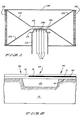
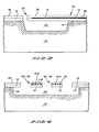
- Figures 2 and 3 are cross-sectional side views of alternate preferred embodiments of the present flow sensor.
- a monocrystalline semiconductor body 10 has a first surface 14 covered with a dielectric layer 12 such as silicon nitride.
- a dielectric layer 12 such as silicon nitride.
- an element 22 ( Figure 5) comprises a permalloy resistive element or grid 16 and leads 24 sputtered onto dielectric layer 12, element 22 being covered with a layer 18 of dielectric such as silicon nitride.
- Dielectric layer 12 provides electrical isolation between element 22 and semiconductor 10 (layers 12 and 18 also provide passivation for element 22). Substantial thermal and physical isolation is provided between resistive element 16 and semiconductor body 10 by forming a depression 20 below element 16. Depression 20 is typically formed using preferential etching techniques such as those discussed elsewhere herein. Without depression 20, it would be difficult to achieve substantial thermal and physical isolation between sensing element 16 and semiconductor 10. For example, if resistive element 16 were separated from semiconductor 10 by only a solid dielectric layer, resistive element 16 would be substantially heat sunk into semiconductor 10, since the thermal conductivity of solid dielectrics are typically greater than the thermal conductivity of air.
- sensing element 16 and semiconductor 10 provides many advantages. For example, by providing a very thin sensing means that is substantially thermally isolated from the semiconductor body, the sensing means is adapted to provide a very sensitive measurement of air flow since the temperature of the thin structure will be readily affected by the air flow. This is in contrast to solid state thermal anemometers that have sensing elements substantially heat sunk into the semiconductor body. The temperature sensitivity of such structures is greatly affected by the thermal mass of the semiconductor itself.
- member or sensing means 34 is bridged across depression 20, member means 34 having first and second ends 38 and 40 connected to semiconductor first surface 14.
- member means 34 is substantially rectangular in shape when viewed from above, member means 34 as disclosed comprising resistive element 16 and a portion of dielectric layers 12 and 18.
- member or sensing means 32 comprising a resistive element 16 and a portion of dielectric layers 12 and 18 is cantilevered over depression 20, only one end 36 of member means 32 being connected to semiconductor first surface 14. Having only one end of member means 32 connected to semiconductor body 10 provides certain advantages, including the advantage of permitting member means 32 to expand and contract in substantially all directions without substantial restraint from semiconductor body 10.
- member means 32 provides an embodiment having substantially increased thermal isolation because heat loss by conduction through member means 32 occurs only through one supporting end.
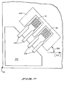
- member means 32 is typically substantially rectangular in shape when viewed from above (for example, see Figure 7).
- Figure 4 illustrates an end cross-sectional view of a preferred embodiment comprising two member means 32 or 34.
- a pair of member means is a preferred embodiment having certain advantages. For example, as is further discussed below, using two substantially identical member means and offsetting a signal from one against a signal from the other can provide automatic temperature compensation for changing environmental temperatures. In addition, such an arrangement can greatly increase measurement accuracy, since background voltage within a single sensor can easily' be substantially eliminated. Further, using two measurement elements in a flow sensor provides an indication of flow direction as well as rate: for example, in a constant current mode of operation of the present sensor, the upstream element cools more than the downstream element, as is further explained below.
- a single sensing means supported over depression 20 is consistent with the present flow sensor; for example, for making a flow/no-flow measurement, an air turbulence signal generated in a single-sensing-element flow sensor would be adequate to establish the presence or the absence of air flow.
- Amplification of only the a.c. (turbulent flow) component of an element resistance change eliminates detection of slow or d.c. changes in element resistance caused, for example, by changing environmental temperature.
- permalloy was selected to form resistive element 16 because permalloy can be precisely deposited by sputtering a layer only hundreds of angstroms thick, and because the characteristics of permalloy provide a highly sensitive predetermined relationship between the resistance of grid or element 16 and the temperature of the element.
- a very thin member or sensing means 32 or 34 may be formed of resistive element 16 and dielectric layers 12 and 18. As such, air flowing over member means 32 or 34 will cause resistive element 16 to cool in predetermined relation to the rate of air flow, thus causing a change in resistance and providing a measurement of the air flow.
- member means 32 and 34 are typically on the order of 0.8 - 1.2 microns thick, this thickness including element 16 (typically on the order of 800 angstroms thick) and dielectric layers 12 and 18, each typically on the order of thousands of angstroms thick.
- This very thin and highly sensitive configuration in combination with the fact that sensing element 16 is substantially isolated from the body of semiconductor 10 by depression 20 (typically in the range of 0.001 to 0.010 inch deep) causes sensing or member means 32 and 34 to be highly sensitive to flow measurements.
- a preferred embodiment of element 16 comprises a permalloy grid as shown in Figure 5.
- Leads 24 may be permalloy since additional processing steps are then avoided (making leads 24 of another material would require additional processing steps; although leads 24 of permalloy become slightly heated, they are relatively wide, as illustrated in Figure 5, and they are substantially heat sunk into semiconductor body 10, making heating of leads 24 relatively minor).
- a flow transducer comprising first and second resistive elements such as illustrated in Figure 4.
- Such an embodiment may be coupled with a circuit such as illustrated in Figure 6, thus providing a flow transducer which is independent of environmental temperatures and which provides further sensitivity by eliminating background signals and directly providing a measurement signal.
- each element 16A and 16E comprising an element 16.
- Element 16A and 16E are typically matched (at least substantially identical) but they do not have to be matched.
- Circuit 60 illustrated in Figure 6 comprises three differential amplifiers, each of which may comprise, for example, a TLC87. As illustrated, each of two amplifiers 50 and 52 have a resistive element 16A or 16E connected across its feedback loop. Thus, resistive element 16A is connected between an output 54 of a negative input 59 of' amplifier 50, the connections being made via leads 24 associated with element 16A. Resistive element 16B is connected across an output 56 and a negative input 58 of amplifier 52, the connections again being made with leads 24 associated with element 16E.
- Negative input 58 to amplifier 52 is connected to a wiper 66 of a potentiometer 62 through a resistor 64.
- Negative input 59 to amplifier 50 is connected to wiper 66 through a resistor 70.
- Positive inputs 72 and 74 of amplifiers 50 and 52, respectively, are connected to ground or reference potential 76.
- Cutput 56 of amplifier 52 is connected to a negative input 58 of amplifier 80 through a resistor 82, output 54 of amplifier 50 being-connected to a positive input 84 to amplifier 80 through a resistor 86.
- Positive input 84 of amplifier 80 is also connected to ground or reference potential 76 through a resistor 88.
- a resistor 90 is connected between an output 92 of amplifier 80 and a negative input 78 of the amplifier.
- a first terminal 94 of potentiometer 62 is provided for connection to a positive power supply such as +15VLC, a second' terminal 96 of potentiometer 62 being provided for connection to a negative power supply such as -15VEC. Potentiometer 62 provides a means for selecting a predetermined voltage anywhere between the plus and minus voltage of the power supply.
- the disclosed circuit In operation, the disclosed circuit generates a voltage between output 92 and ground or reference potential 76 that bears a predetermined relationship to gas flow rate over the two member means 32 or 34 comprising resistive elements 16A and 16B.
- Resistive elements 16A and 16B are configured into the feedback loops of amplifiers 50 and 52, respectively.
- Each operational amplifier 50 and 52 maintains constant current through its feedback loop. Therefore, the electrical current flowing through each resistive element 16A and 16E is independent of the element resistance.
- each operational amplifier in effect changes its output voltage in proportion to the change in resistance of resistive element 16A or 16B.
- each permalloy element 16A or 16E changes in a predetermined manner with the temperature of the resistive element. Therefore, the voltage output of each operational amplifier 50 and 52 bears a predetermined relationship to the associated resistive element temperature. (As discussed further below, modes of operation other than constant current are also possible).
- Operational amplifier 80 amplifies the difference between the voltage outputs of operational amplifiers 50 and 52, the voltage at output 92 being proportional to the difference in voltage between the output voltages of operational amplifiers 50 and 52. Accordingly., the voltage at output 92 bears a predetermined relationship to the temperature difference between resistive elements 16A and 16B. The temperature difference between resistive elements 16A and 16B bears a predetermined relationship to the gas flow rate over the elements. Therefore, the voltage at output 92 of amplifier 80 bears a predetermined relationship to the rate of flow across elements 16A and 16E.
- the present two element sensor can be used to determine direction of flow as well as flow rate, since the upstream element will cool more than the downstream element, as explained above.
- circuit illustrated in Figure 6 operates sensing elements 16A and 16B in a constant current mode.
- Other circuits are also possible, including circuits which operate the sensing element or elements of the present flow sensor in a constant voltage mode, a constant temperature (constant resistance) mode, or a constant power mode.
- Circuits such as 60 illustrated in Figure 6 may be integrated directly onto semiconductor body 10 as schematically illustrated in Figure 7.
- the present flow sensor can be fabricated through batch processing as further described below.
- a preferred implementation of fabricating the present sensor comprises providing a (100) silicon wafer surface 14 which receives a layer of silicon nitride 12 typically 3000 angstroms thick that is deposited by standard sputtering techniques in a low pressure gas discharge. Next, a uniform layer of permalloy, typically 80 percent nickel or and 20 percent iroh and 800 angstroms thick, is deposited on the silicon nitride by sputtering.
- the permalloy element 22 comprising grid 16 and leads 24 are delineated.
- a second layer 18 of silicon nitride is then sputtered-deposited to provide complete step coverage of the permalloy configuration and thus protect the resistive element and its connections from oxidization.
- a second layer 18 of silicon nitride is then sputtered-deposited to provide complete step coverage of the permalloy configuration and thus protect the resistive element and its connections from oxidization.
- Cne or more openings 152 are then etched through the nitride to the (100) silicon surface in order to delineate each member means.
- the member means 32 or 34 typically have straight edges, such configurations could be varied by, for example, having curved edges.
- anisotropic etchant that does not attack the silicon nitride is used to etch out the silicon in a controlled manner from beneath the member means 32 or 34 (KCH plus isopropyl alcohol is a suitable etchant).
- KCH plus isopropyl alcohol is a suitable etchant.
- the sloping sides of the etched depression are bounded by (111) and other crystal surfaces that are resistive to the etchant, and the bottom of the depression, a (100) surface which is much less resistant to the etchant, is located a specified distance, e.g., 0.004 inch, from the member means, typically by adjusting the duration of the etch.
- a doped silicon etch stop e.g., a boron-doped layer, may also be used to control the depth of the depression, although such stops are typically not necessary when using the present process.
- the predetermined configuration of the member means e.g., typically straight edge or an axis of the member means, is oriented at a non-zero angle 154 ( Figure 7) to the [110] axis of the silicon.
- a non-zero angle 154 Figure 7
- the member means will be undercut in a minimum amount of time.
- a cantilever beam of the typical dimensions disclosed elsewhere herein can be undercut in about 90 minutes by comparison to an etched time of several hours using a zero degree orientation.
- Etch holes 152 running along the side of member means 32 or 34 have typical widths on the order of 0.002 inch to 0.005 inch. Typical dimensions of widths on the order of 0.002 inch to 0.005 inch. Typical dimensions of member means such as 32 or 34 are 0.005 inch - 0.007 inch wide, 0.010 - 0.020 inch long, and 0.8 - 1.2 microns thick. Typical permalloy elements such as element 16 illustrated in Figure 5 have a thickness of approximately 800 angstroms (typically in the range of approximately 800 angstroms to approximately 1600 angstroms) with a preferred composition of 80 percent nickel and 20 percent iron and a resistance value of about 1000 ohms at room temperature.
- Resistance values for varying applications would typically be within the range of approximately 500 ohms to approximately 2000 ohms at room temperature, e.g., approximately 25°C (at permalloy element temperatures up to approximately 400°C, resistance values increased by a factor of up to approximately 3.0).
- Line widths within permalloy grid 16 may be approximately 6 microns having a 4 micron spacing.
- Depressions such as 20 typically have a 0.004 inch spacing between member means 32 or 34 and semiconductor body 10, but such spacing could easily vary in the range of approximately 0.001 inch to approximately 0.010 inch.
- a typical thickness of semiconductor body or substrate 10 is 0.008 inch. (The dimensions provided are illustrative only and are not to be taken as limitations).
- the strength-to-weight ratio for a flow sensor as described is very favorable, and a two-ended bridge of the above typical dimensions can withstand mechanical shock forces well in excess of 10,000 gravities. Even a single-ended ' structure of these dimensions when treated as a cantilever beam can be shown to withstand 10,000 gravities of shock.
- housing portions 104 need not be a smooth taper; virtually any configuration of the volume between filters 102 and housing portions 106 will work.
- portions 104 could be right circular cylinders having a filter 102 enclosing one end and being enclosed at the other end except for a small hole corresponding in area to the cross-sectional area of orifice 106.
Landscapes
- Physics & Mathematics (AREA)
- Fluid Mechanics (AREA)
- General Physics & Mathematics (AREA)
- Measuring Volume Flow (AREA)
- Filtering Of Dispersed Particles In Gases (AREA)
Applications Claiming Priority (2)
| Application Number | Priority Date | Filing Date | Title |
|---|---|---|---|
| US36412782A | 1982-03-31 | 1982-03-31 | |
| US364127 | 1982-03-31 |
Publications (1)
| Publication Number | Publication Date |
|---|---|
| EP0094497A1 true EP0094497A1 (fr) | 1983-11-23 |
Family
ID=23433131
Family Applications (1)
| Application Number | Title | Priority Date | Filing Date |
|---|---|---|---|
| EP83103015A Withdrawn EP0094497A1 (fr) | 1982-03-31 | 1983-03-26 | Appareil de détection de courants gazeux |
Country Status (2)
| Country | Link |
|---|---|
| EP (1) | EP0094497A1 (fr) |
| JP (1) | JPS58183920A (fr) |
Cited By (15)
| Publication number | Priority date | Publication date | Assignee | Title |
|---|---|---|---|---|
| US4785662A (en) * | 1984-04-26 | 1988-11-22 | Nippon Soken, Inc. | Direct-heated gas-flow measuring apparatus |
| US4833912A (en) * | 1987-01-19 | 1989-05-30 | Nippon Soken, Inc. | Flow measuring apparatus |
| DE4219454A1 (de) * | 1992-06-13 | 1993-12-16 | Bosch Gmbh Robert | Massenflußsensor |
| WO1995017651A1 (fr) * | 1993-12-23 | 1995-06-29 | Honeywell Inc. | Ensemble capteur de debit muni de deux limiteurs integres |
| DE10327934B3 (de) * | 2003-06-20 | 2005-02-24 | Dräger Medical AG & Co. KGaA | Messvorrichtung zur Messung des Durchflusses und/oder von Stoffeigenschaften eines Gasstroms |
| CN101061288B (zh) * | 2004-04-06 | 2011-04-13 | 福罗西内空间体系有限公司 | 筒套 |
| GB2479040A (en) * | 2010-03-22 | 2011-09-28 | Honeywell Int Inc | Sensor assembly with hydrophobic filter |
| US8397586B2 (en) | 2010-03-22 | 2013-03-19 | Honeywell International Inc. | Flow sensor assembly with porous insert |
| US8656772B2 (en) | 2010-03-22 | 2014-02-25 | Honeywell International Inc. | Flow sensor with pressure output signal |
| US8695417B2 (en) | 2011-01-31 | 2014-04-15 | Honeywell International Inc. | Flow sensor with enhanced flow range capability |
| US8756990B2 (en) | 2010-04-09 | 2014-06-24 | Honeywell International Inc. | Molded flow restrictor |
| US9003877B2 (en) | 2010-06-15 | 2015-04-14 | Honeywell International Inc. | Flow sensor assembly |
| US9052217B2 (en) | 2012-11-09 | 2015-06-09 | Honeywell International Inc. | Variable scale sensor |
| US9091577B2 (en) | 2011-01-31 | 2015-07-28 | Honeywell International Inc. | Flow sensor assembly with integral bypass channel |
| US9952079B2 (en) | 2015-07-15 | 2018-04-24 | Honeywell International Inc. | Flow sensor |
Citations (3)
| Publication number | Priority date | Publication date | Assignee | Title |
|---|---|---|---|---|
| US3433069A (en) * | 1965-10-01 | 1969-03-18 | Technology Inc | Mass flowmeter structure |
| US3881181A (en) * | 1973-02-22 | 1975-04-29 | Rca Corp | Semiconductor temperature sensor |
| US3962917A (en) * | 1974-07-03 | 1976-06-15 | Minato Medical Science Co., Ltd. | Respirometer having thermosensitive elements on both sides of a hot wire |
Family Cites Families (4)
| Publication number | Priority date | Publication date | Assignee | Title |
|---|---|---|---|---|
| JPS5122745A (ja) * | 1974-08-16 | 1976-02-23 | Sumitomo Chemical Co | Horiorefuinkeijushisoseibutsu |
| JPS5953489B2 (ja) * | 1977-05-30 | 1984-12-25 | 横河電機株式会社 | 流速流量測定装置 |
| JPS5469473A (en) * | 1977-11-14 | 1979-06-04 | Yokogawa Hokushin Electric Corp | Measuring apparatus of velocity and rate of flow |
| JPS55112521A (en) * | 1979-01-23 | 1980-08-30 | Osaka Gas Co Ltd | Flow speed measuring method |
-
1983
- 1983-03-26 EP EP83103015A patent/EP0094497A1/fr not_active Withdrawn
- 1983-03-31 JP JP5676283A patent/JPS58183920A/ja active Pending
Patent Citations (3)
| Publication number | Priority date | Publication date | Assignee | Title |
|---|---|---|---|---|
| US3433069A (en) * | 1965-10-01 | 1969-03-18 | Technology Inc | Mass flowmeter structure |
| US3881181A (en) * | 1973-02-22 | 1975-04-29 | Rca Corp | Semiconductor temperature sensor |
| US3962917A (en) * | 1974-07-03 | 1976-06-15 | Minato Medical Science Co., Ltd. | Respirometer having thermosensitive elements on both sides of a hot wire |
Cited By (22)
| Publication number | Priority date | Publication date | Assignee | Title |
|---|---|---|---|---|
| US4785662A (en) * | 1984-04-26 | 1988-11-22 | Nippon Soken, Inc. | Direct-heated gas-flow measuring apparatus |
| US4833912A (en) * | 1987-01-19 | 1989-05-30 | Nippon Soken, Inc. | Flow measuring apparatus |
| DE4219454A1 (de) * | 1992-06-13 | 1993-12-16 | Bosch Gmbh Robert | Massenflußsensor |
| US5404753A (en) * | 1992-06-13 | 1995-04-11 | Robert Bosch Gmbh | Mass flow sensor |
| WO1995017651A1 (fr) * | 1993-12-23 | 1995-06-29 | Honeywell Inc. | Ensemble capteur de debit muni de deux limiteurs integres |
| US5581027A (en) * | 1993-12-23 | 1996-12-03 | Honeywell Inc. | Dual integral ballast flow sensor |
| DE10327934B3 (de) * | 2003-06-20 | 2005-02-24 | Dräger Medical AG & Co. KGaA | Messvorrichtung zur Messung des Durchflusses und/oder von Stoffeigenschaften eines Gasstroms |
| CN101061288B (zh) * | 2004-04-06 | 2011-04-13 | 福罗西内空间体系有限公司 | 筒套 |
| GB2479040B (en) * | 2010-03-22 | 2012-06-20 | Honeywell Int Inc | Sensor assembly with hydrophobic filter |
| US8656772B2 (en) | 2010-03-22 | 2014-02-25 | Honeywell International Inc. | Flow sensor with pressure output signal |
| GB2479040A (en) * | 2010-03-22 | 2011-09-28 | Honeywell Int Inc | Sensor assembly with hydrophobic filter |
| GB2487497A (en) * | 2010-03-22 | 2012-07-25 | Honeywell Int Inc | Sensor assembly with filter |
| US8397586B2 (en) | 2010-03-22 | 2013-03-19 | Honeywell International Inc. | Flow sensor assembly with porous insert |
| GB2487497B (en) * | 2010-03-22 | 2013-07-10 | Honeywell Int Inc | Sensor assembly with filter |
| US8485031B2 (en) | 2010-03-22 | 2013-07-16 | Honeywell International Inc. | Sensor assembly with hydrophobic filter |
| US8113046B2 (en) | 2010-03-22 | 2012-02-14 | Honeywell International Inc. | Sensor assembly with hydrophobic filter |
| US8756990B2 (en) | 2010-04-09 | 2014-06-24 | Honeywell International Inc. | Molded flow restrictor |
| US9003877B2 (en) | 2010-06-15 | 2015-04-14 | Honeywell International Inc. | Flow sensor assembly |
| US8695417B2 (en) | 2011-01-31 | 2014-04-15 | Honeywell International Inc. | Flow sensor with enhanced flow range capability |
| US9091577B2 (en) | 2011-01-31 | 2015-07-28 | Honeywell International Inc. | Flow sensor assembly with integral bypass channel |
| US9052217B2 (en) | 2012-11-09 | 2015-06-09 | Honeywell International Inc. | Variable scale sensor |
| US9952079B2 (en) | 2015-07-15 | 2018-04-24 | Honeywell International Inc. | Flow sensor |
Also Published As
| Publication number | Publication date |
|---|---|
| JPS58183920A (ja) | 1983-10-27 |
Similar Documents
| Publication | Publication Date | Title |
|---|---|---|
| US4472239A (en) | Method of making semiconductor device | |
| EP0094497A1 (fr) | Appareil de détection de courants gazeux | |
| US4624137A (en) | Semiconductor device | |
| KR960015067B1 (ko) | 실리콘 베이스 질량 기류 센서 및 그 조립방법 | |
| US4548078A (en) | Integral flow sensor and channel assembly | |
| US4581928A (en) | Slotted diaphragm semiconductor device | |
| US5291781A (en) | Diaphragm-type sensor | |
| EP1992917B1 (fr) | Débitmètre thermique | |
| EP0395721B1 (fr) | Circuits de commande et de detection pour capteurs d'ecoulement massique d'air | |
| US4683159A (en) | Semiconductor device structure and processing | |
| JP3302444B2 (ja) | 質量流量センサ | |
| EP2600121B1 (fr) | Débitmètre thermique | |
| EP0076935B1 (fr) | Dispositif semiconducteur intégré et son procédé de fabrication | |
| US4867842A (en) | Method of making slotted diaphragm semiconductor devices | |
| US4825693A (en) | Slotted diaphragm semiconductor device | |
| US20020020689A1 (en) | Accelerometer without proof mass | |
| KR20010014671A (ko) | 감열식 유량센서 | |
| US6725716B1 (en) | Thermo-sensitive flow rate sensor and method of manufacturing the same | |
| US5201221A (en) | Flow sensor and method of manufacture | |
| EP0176996B1 (fr) | Dispositif semi-conducteur, en particulier capteur à semi-conducteur et son procédé de fabrication | |
| JPH0352028B2 (fr) | ||
| EP0452134B1 (fr) | Capteur du type à diaphragme | |
| EP0169519B1 (fr) | Dispositif semi-conducteur et son procédé de fabrication | |
| EP0134859A1 (fr) | Capteur de débit de liquide | |
| CA1273227A (fr) | Dispositif semiconducteur a diaphragme a fentes |
Legal Events
| Date | Code | Title | Description |
|---|---|---|---|
| PUAI | Public reference made under article 153(3) epc to a published international application that has entered the european phase |
Free format text: ORIGINAL CODE: 0009012 |
|
| AK | Designated contracting states |
Designated state(s): DE FR GB NL |
|
| STAA | Information on the status of an ep patent application or granted ep patent |
Free format text: STATUS: THE APPLICATION IS DEEMED TO BE WITHDRAWN |
|
| 18D | Application deemed to be withdrawn |
Effective date: 19840724 |
|
| RIN1 | Information on inventor provided before grant (corrected) |
Inventor name: JOHNSON, ROBERT G. Inventor name: BOHRER, PHILIP J. |