EP0094545A1 - Verfahren und Vorrichtung zur Überwachung der Ablagerungsgeschwindigkeit - Google Patents
Verfahren und Vorrichtung zur Überwachung der Ablagerungsgeschwindigkeit Download PDFInfo
- Publication number
- EP0094545A1 EP0094545A1 EP83104282A EP83104282A EP0094545A1 EP 0094545 A1 EP0094545 A1 EP 0094545A1 EP 83104282 A EP83104282 A EP 83104282A EP 83104282 A EP83104282 A EP 83104282A EP 0094545 A1 EP0094545 A1 EP 0094545A1
- Authority
- EP
- European Patent Office
- Prior art keywords
- output
- detector
- rate
- deposition
- sensor
- Prior art date
- Legal status (The legal status is an assumption and is not a legal conclusion. Google has not performed a legal analysis and makes no representation as to the accuracy of the status listed.)
- Granted
Links
- 230000008021 deposition Effects 0.000 title claims abstract description 28
- 238000000034 method Methods 0.000 title claims abstract description 17
- 238000012544 monitoring process Methods 0.000 title claims abstract description 12
- 238000012360 testing method Methods 0.000 claims abstract description 6
- 238000005137 deposition process Methods 0.000 claims abstract description 4
- 238000005259 measurement Methods 0.000 claims description 5
- 230000011664 signaling Effects 0.000 claims 1
- 238000007747 plating Methods 0.000 abstract description 24
- 238000007772 electroless plating Methods 0.000 abstract description 7
- 238000000151 deposition Methods 0.000 description 17
- 238000010899 nucleation Methods 0.000 description 5
- 230000000977 initiatory effect Effects 0.000 description 3
- 239000000523 sample Substances 0.000 description 3
- 230000000694 effects Effects 0.000 description 2
- 238000007654 immersion Methods 0.000 description 2
- 239000007788 liquid Substances 0.000 description 2
- 239000002184 metal Substances 0.000 description 2
- 239000012811 non-conductive material Substances 0.000 description 2
- 239000000725 suspension Substances 0.000 description 2
- 238000001771 vacuum deposition Methods 0.000 description 2
- 238000012512 characterization method Methods 0.000 description 1
- 238000000576 coating method Methods 0.000 description 1
- 230000001419 dependent effect Effects 0.000 description 1
- 238000006073 displacement reaction Methods 0.000 description 1
- 239000002245 particle Substances 0.000 description 1
- 239000000126 substance Substances 0.000 description 1
- 230000000007 visual effect Effects 0.000 description 1
Images
Classifications
-
- G—PHYSICS
- G01—MEASURING; TESTING
- G01B—MEASURING LENGTH, THICKNESS OR SIMILAR LINEAR DIMENSIONS; MEASURING ANGLES; MEASURING AREAS; MEASURING IRREGULARITIES OF SURFACES OR CONTOURS
- G01B7/00—Measuring arrangements characterised by the use of electric or magnetic techniques
- G01B7/02—Measuring arrangements characterised by the use of electric or magnetic techniques for measuring length, width or thickness
- G01B7/06—Measuring arrangements characterised by the use of electric or magnetic techniques for measuring length, width or thickness for measuring thickness
- G01B7/10—Measuring arrangements characterised by the use of electric or magnetic techniques for measuring length, width or thickness for measuring thickness using magnetic means, e.g. by measuring change of reluctance
- G01B7/105—Measuring arrangements characterised by the use of electric or magnetic techniques for measuring length, width or thickness for measuring thickness using magnetic means, e.g. by measuring change of reluctance for measuring thickness of coating
Definitions
- This invention relates generally to conductive film deposition rate monitors and more particularly to a method and apparatus for monitoring the deposition rate and thickness of deposition in a metallic deposition environment, particularly in an electroless (non-electrolytic) plating bath.
- Plating thickness measuring devices are known in the art. Such devices are usually employed to determine the thickness of a plating after it has been deposited; i.e., as a post-plating measurement. Also the use of eddy current devices to measure metallic deposition thickness is well known. In electroless plating, there are many varying factors which determine the degree of success to be achieved in the plating operation. One important factor is the rate of plating.
- the present invention provides a deposition rate monitoring method and apparatus which measure the real time deposition rate of a metallic deposition process, particularly an electroless plating bath, including the step of positioning an eddy current proximity detector within a predetermined distance of a test surface where the deposition is to be deposited and the step of monitoring the output of the detector.
- the apparatus comprises an eddy current proximity sensor and a non-metallic housing or cap for the sensor, having a non-conductive wall of predetermined thickness between the sensor and the surface of the wall distant from the sensor, the distant wall being immersed in the deposition environment, such as a plating bath, so that a deposit takes place on the distant surface, and measuring means connected to the output of the sensor for measuring the amplitude and rate of change of the output of the sensor.
- this invention will provide a method and means to test seeding processes and plating initiation.
- Another object of the invention is to provide an improved plating rate monitor which operates in real time and in the bath itself.
- a further object of the invention is to provide an improved plating rate monitor which operates in real time on a continuing basis.
- Another object of the invention is to provide an improved method and means for testing seeding processes and plating initiation.
- an eddy current proximity detector is positioned at a predetermined distance from a surface on which metallic deposition can take place.
- the assembly is placed in the deposition environment and the output of the proximity detector is monitored with respect to the amplitude and the rate of change of the output, thereby indicating the thickness of the deposition and the rate at which it is being deposited.
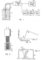
- a plating bath 3 comprises a plating liquid body 5 enclosed in a suitable container, a portion of which container wall is shown at 7.
- a bracket 9 or other suspension device an eddy current sensing probe 11 is suspended at a suitable distance beneath the surface of the plating bath, for example, of the order of 15 cm (6 inches).
- a liquid-proof housing is provided for the sensing element including a cap 13, the details of which will be subsequently explained, and a liquid-proof connecting cable 15 is provided, which also acts as a suspension for the sensor.
- the output leads from the sensor are supplied to the input of a detector driver unit 17, which will produce an output signal which will have an amplitude and rate of change that is dependent upon the thickness and rate at which a metallic deposit is deposited onto the cap 13.
- eddy current sensor unit 11 The details of the eddy current sensor unit 11 and the associated detector driver unit 17 are not shown, since they may take any number of forms well known in the art.
- One such type of eddy current sensor device is manufactured by the Bently-Nevada Corporation, and is a regular commercially available item.
- the output of the detector driver unit 17 is supplied, for example, to the input of a conventional strip chart recorder 19 and may also be supplied, via an analog to digital converter 21, to the input of a microcomputer 23, the output of which is in turn connected to an output device 25, which may be, for example, a visual display, a recording device, or an output printer.
- the eddy current probe or sensor 11 comprises a body element of non-conductive material enclosing a coil which when energized will produce eddy currents in any metallic surface nearby, the effect of the eddy currents being determined by the detector driver unit 17 of Fig. 1.
- the sensor 11 is threaded for all or a greater portion of its length and is provided with a cap 13 of non-magnetic, non-conductive material having an internal thread which corresponds to the threads on the sensor 11.
- the lower wall of the cap 13 has a predetermined thickness designated by d of known and accurately measured amount.
- the cap 13 is screwed onto to the sensor 11, and the assembly is rendered liquid-proof by any suitable means, such as a rubber enclosure or other arrangement to protect the assembly from liquid except for the lower wall.
- Fig. 3 is a dimensionless graph showing the relationship between time, starting with the immersion of the sensor, and the eddy current loss as measured by the sensing device.
- the initial portion of the curve designated as "seeding effectiveness", indicates the time from the immersion of the probe to the time, at 35, when plating commences. This time appears to be an indicator of (1) seeding effectiveness (using different methods), and (2) plating bath solution activity (varying chemical parameters). Suitable characterization or standardization of either of these factors will enable study of the variation of the other factor.
- the portion of the curve which rises from 35 to a peak value at 37, is the segment used for measurement of initiation of the plating operation. It can be seen that a high resolution is obtained with this curve and the rate, of course, is proportional to the slope of the curve.
- the central portion of the curve is the section which is used for thickness measurement of coatings after a plating operation has taken place, while the very right hand portion with, in the present instance, substantially zero slope is commonly used for displacement measurements with eddy current sensors by using thick conductive targets and a varying airgap.
- FIG. 4 shows the use of the invention with a conventional vacuum deposition system.
- a vacuum chamber 19 contains a source 21 of metallic vapor or particles, which are directed to an object 23 on which a metal layer is to be deposited.
- the sensor 11, 13 is inserted in the chamber as shown, and metal is also deposited on the sensor.
- the remainder of the apparatus, its operation and characteristics are similar to those decribed above.
- the present invention provides an improved method and apparatus for determining the thickness of plating being provided in an electroless plating bath or other deposition environment as well as the rate of deposition.
Landscapes
- Physics & Mathematics (AREA)
- General Physics & Mathematics (AREA)
- Measurement Of Length, Angles, Or The Like Using Electric Or Magnetic Means (AREA)
- Chemically Coating (AREA)
- Investigating Or Analyzing Materials By The Use Of Magnetic Means (AREA)
Applications Claiming Priority (2)
| Application Number | Priority Date | Filing Date | Title |
|---|---|---|---|
| US378697 | 1982-05-17 | ||
| US06/378,697 US4556845A (en) | 1982-05-17 | 1982-05-17 | Method for monitoring deposition rate using an eddy current detector |
Publications (2)
| Publication Number | Publication Date |
|---|---|
| EP0094545A1 true EP0094545A1 (de) | 1983-11-23 |
| EP0094545B1 EP0094545B1 (de) | 1987-01-07 |
Family
ID=23494185
Family Applications (1)
| Application Number | Title | Priority Date | Filing Date |
|---|---|---|---|
| EP83104282A Expired EP0094545B1 (de) | 1982-05-17 | 1983-05-02 | Verfahren und Vorrichtung zur Überwachung der Ablagerungsgeschwindigkeit |
Country Status (4)
| Country | Link |
|---|---|
| US (1) | US4556845A (de) |
| EP (1) | EP0094545B1 (de) |
| JP (1) | JPS58201003A (de) |
| DE (1) | DE3368981D1 (de) |
Cited By (1)
| Publication number | Priority date | Publication date | Assignee | Title |
|---|---|---|---|---|
| EP2495357A2 (de) | 2010-11-25 | 2012-09-05 | Technische Universität Dresden | Einrichtung und Verfahren zur Messung der Geschwindigkeit oder der Stromausbeute bei der Abscheidung oder beim Abtrag von Oberflächen und zur darauf basierenden Prozesssteuerung |
Families Citing this family (44)
| Publication number | Priority date | Publication date | Assignee | Title |
|---|---|---|---|---|
| US5200047A (en) * | 1985-02-28 | 1993-04-06 | C. Uyemura & Co., Ltd. | Plating solution automatic control |
| JPS61199069A (ja) * | 1985-02-28 | 1986-09-03 | C Uyemura & Co Ltd | めっき液濃度自動連続管理装置 |
| CA2043347A1 (en) * | 1990-05-30 | 1991-12-01 | Yukio Kohmura | Method and system for inspection of electroconductive film using eddy current and process and system for production of optical fibres using method and system |
| JP2638283B2 (ja) * | 1990-10-17 | 1997-08-06 | 日立化成工業株式会社 | 無電解めっき析出速度測定装置 |
| US5559428A (en) * | 1995-04-10 | 1996-09-24 | International Business Machines Corporation | In-situ monitoring of the change in thickness of films |
| US5660672A (en) * | 1995-04-10 | 1997-08-26 | International Business Machines Corporation | In-situ monitoring of conductive films on semiconductor wafers |
| US6924641B1 (en) * | 2000-05-19 | 2005-08-02 | Applied Materials, Inc. | Method and apparatus for monitoring a metal layer during chemical mechanical polishing |
| US6878038B2 (en) * | 2000-07-10 | 2005-04-12 | Applied Materials Inc. | Combined eddy current sensing and optical monitoring for chemical mechanical polishing |
| US6602724B2 (en) * | 2000-07-27 | 2003-08-05 | Applied Materials, Inc. | Chemical mechanical polishing of a metal layer with polishing rate monitoring |
| US6608495B2 (en) | 2001-03-19 | 2003-08-19 | Applied Materials, Inc. | Eddy-optic sensor for object inspection |
| US6966816B2 (en) | 2001-05-02 | 2005-11-22 | Applied Materials, Inc. | Integrated endpoint detection system with optical and eddy current monitoring |
| US6811466B1 (en) * | 2001-12-28 | 2004-11-02 | Applied Materials, Inc. | System and method for in-line metal profile measurement |
| US7001242B2 (en) | 2002-02-06 | 2006-02-21 | Applied Materials, Inc. | Method and apparatus of eddy current monitoring for chemical mechanical polishing |
| US6937915B1 (en) * | 2002-03-28 | 2005-08-30 | Lam Research Corporation | Apparatus and methods for detecting transitions of wafer surface properties in chemical mechanical polishing for process status and control |
| DE10222049A1 (de) * | 2002-05-17 | 2003-12-18 | Zeiss Carl Laser Optics Gmbh | Verfahren und Vorrichtung zum variablen Abschwächen der Intensität eines Lichtstrahls |
| US20040011462A1 (en) * | 2002-06-28 | 2004-01-22 | Lam Research Corporation | Method and apparatus for applying differential removal rates to a surface of a substrate |
| US7205166B2 (en) * | 2002-06-28 | 2007-04-17 | Lam Research Corporation | Method and apparatus of arrayed, clustered or coupled eddy current sensor configuration for measuring conductive film properties |
| US7128803B2 (en) * | 2002-06-28 | 2006-10-31 | Lam Research Corporation | Integration of sensor based metrology into semiconductor processing tools |
| US6808590B1 (en) | 2002-06-28 | 2004-10-26 | Lam Research Corporation | Method and apparatus of arrayed sensors for metrological control |
| US6929531B2 (en) | 2002-09-19 | 2005-08-16 | Lam Research Corporation | System and method for metal residue detection and mapping within a multi-step sequence |
| US7084621B2 (en) * | 2002-09-25 | 2006-08-01 | Lam Research Corporation | Enhancement of eddy current based measurement capabilities |
| US6788050B2 (en) | 2002-12-23 | 2004-09-07 | Lam Research Corp. | System, method and apparatus for thin-film substrate signal separation using eddy current |
| US7016795B2 (en) * | 2003-02-04 | 2006-03-21 | Applied Materials Inc. | Signal improvement in eddy current sensing |
| US6945845B2 (en) * | 2003-03-04 | 2005-09-20 | Applied Materials, Inc. | Chemical mechanical polishing apparatus with non-conductive elements |
| US7112960B2 (en) | 2003-07-31 | 2006-09-26 | Applied Materials, Inc. | Eddy current system for in-situ profile measurement |
| US7025658B2 (en) * | 2003-08-18 | 2006-04-11 | Applied Materials, Inc. | Platen and head rotation rates for monitoring chemical mechanical polishing |
| US20050050970A1 (en) * | 2003-09-08 | 2005-03-10 | Delphi Technologies, Inc. | Cap assembly for sealing system and method of assembling same |
| CN100564592C (zh) * | 2003-09-19 | 2009-12-02 | 应用材料公司 | 对无电沉积的终点进行检测的装置和方法 |
| US20050066739A1 (en) * | 2003-09-26 | 2005-03-31 | Lam Research Corporation | Method and apparatus for wafer mechanical stress monitoring and wafer thermal stress monitoring |
| US20050083048A1 (en) * | 2003-10-21 | 2005-04-21 | Applied Materials, Inc. | Plating system with integrated substrate inspection |
| US6955588B1 (en) | 2004-03-31 | 2005-10-18 | Lam Research Corporation | Method of and platen for controlling removal rate characteristics in chemical mechanical planarization |
| US20060062897A1 (en) * | 2004-09-17 | 2006-03-23 | Applied Materials, Inc | Patterned wafer thickness detection system |
| US8337278B2 (en) | 2007-09-24 | 2012-12-25 | Applied Materials, Inc. | Wafer edge characterization by successive radius measurements |
| JP5611214B2 (ja) | 2008-10-16 | 2014-10-22 | アプライド マテリアルズ インコーポレイテッドApplied Materials,Incorporated | 渦電流利得の補償 |
| JP5615831B2 (ja) * | 2008-11-14 | 2014-10-29 | アプライド マテリアルズ インコーポレイテッドApplied Materials,Incorporated | 縁部分解能強化渦電流センサ |
| JP5759231B2 (ja) * | 2011-04-04 | 2015-08-05 | 日東電工株式会社 | めっき装置、めっき方法および配線回路基板の製造方法 |
| DE102011084903A1 (de) * | 2011-10-20 | 2013-04-25 | TAKATA Aktiengesellschaft | Sensorsysteme für ein Kraftfahrzeug |
| CN106414215B (zh) | 2014-05-22 | 2020-03-17 | Tk控股公司 | 用于屏蔽方向盘中的手传感器系统的系统和方法 |
| CN111422238B (zh) | 2014-06-02 | 2022-10-25 | Tk控股公司 | 用于在方向盘的传感器垫上印刷传感器电路的系统和方法 |
| US10336361B2 (en) | 2016-04-04 | 2019-07-02 | Joyson Safety Systems Acquisition Llc | Vehicle accessory control circuit |
| WO2018080764A1 (en) | 2016-10-28 | 2018-05-03 | Applied Materials, Inc. | Core configuration with alternating posts for in-situ electromagnetic induction monitoring system |
| US12098918B2 (en) | 2020-08-25 | 2024-09-24 | Corning Incorporated | In-situ deposition thickness monitoring |
| CN120020280A (zh) * | 2023-11-20 | 2025-05-20 | 盛美半导体设备(上海)股份有限公司 | 电镀方法及电镀装置 |
| DE102024119448A1 (de) * | 2024-07-09 | 2026-01-15 | SURAGUS GmbH | Messvorrichtung zur Charakterisierung eines Messobjektes im Vakuum mittels induktivem Sensor in elektromagnetischer Transmission |
Citations (4)
| Publication number | Priority date | Publication date | Assignee | Title |
|---|---|---|---|---|
| US2916694A (en) * | 1956-03-02 | 1959-12-08 | Gen Motors Corp | Coating thickness gage |
| US3358225A (en) * | 1964-03-27 | 1967-12-12 | Richard S Peugeot | Lift-off compensation for eddy current testers |
| FR1565789A (de) * | 1967-04-12 | 1969-05-02 | ||
| DE2219622A1 (de) * | 1971-05-11 | 1972-11-16 | N.V. Philips Gloeilampenfabrieken, Eindhoven (Niederlande) | Verfahren und Anordnung zum Bestimmen der Dicke einer Schicht dielektrischen Materials während ihres Anwuchses |
Family Cites Families (3)
| Publication number | Priority date | Publication date | Assignee | Title |
|---|---|---|---|---|
| US3230447A (en) * | 1961-11-01 | 1966-01-18 | Bunker Ramo | Magnetic plating monitoring device |
| US3773548A (en) * | 1972-01-27 | 1973-11-20 | Optical Coating Laboratory Inc | Method of monitoring the rate of depositing a coating solely by its optical properties |
| JPS56117103A (en) * | 1980-02-21 | 1981-09-14 | Toshiba Corp | Measuring device for vapor-deposition quantity of liquid metal |
-
1982
- 1982-05-17 US US06/378,697 patent/US4556845A/en not_active Expired - Lifetime
-
1983
- 1983-03-16 JP JP58042511A patent/JPS58201003A/ja active Granted
- 1983-05-02 EP EP83104282A patent/EP0094545B1/de not_active Expired
- 1983-05-02 DE DE8383104282T patent/DE3368981D1/de not_active Expired
Patent Citations (4)
| Publication number | Priority date | Publication date | Assignee | Title |
|---|---|---|---|---|
| US2916694A (en) * | 1956-03-02 | 1959-12-08 | Gen Motors Corp | Coating thickness gage |
| US3358225A (en) * | 1964-03-27 | 1967-12-12 | Richard S Peugeot | Lift-off compensation for eddy current testers |
| FR1565789A (de) * | 1967-04-12 | 1969-05-02 | ||
| DE2219622A1 (de) * | 1971-05-11 | 1972-11-16 | N.V. Philips Gloeilampenfabrieken, Eindhoven (Niederlande) | Verfahren und Anordnung zum Bestimmen der Dicke einer Schicht dielektrischen Materials während ihres Anwuchses |
Cited By (1)
| Publication number | Priority date | Publication date | Assignee | Title |
|---|---|---|---|---|
| EP2495357A2 (de) | 2010-11-25 | 2012-09-05 | Technische Universität Dresden | Einrichtung und Verfahren zur Messung der Geschwindigkeit oder der Stromausbeute bei der Abscheidung oder beim Abtrag von Oberflächen und zur darauf basierenden Prozesssteuerung |
Also Published As
| Publication number | Publication date |
|---|---|
| JPS58201003A (ja) | 1983-11-22 |
| US4556845A (en) | 1985-12-03 |
| EP0094545B1 (de) | 1987-01-07 |
| JPH0242401B2 (de) | 1990-09-21 |
| DE3368981D1 (en) | 1987-02-12 |
Similar Documents
| Publication | Publication Date | Title |
|---|---|---|
| EP0094545A1 (de) | Verfahren und Vorrichtung zur Überwachung der Ablagerungsgeschwindigkeit | |
| US5051921A (en) | Method and apparatus for detecting liquid composition and actual liquid level | |
| US4051431A (en) | Apparatus for measuring rates of urine flow electrically | |
| US4470300A (en) | Apparatus for and method of determining a capacitance | |
| US4675662A (en) | Machine oil deterioration detection | |
| US12098995B2 (en) | Method and measuring arrangement for determining the internal corrosion rate of steel structures | |
| EP0417936B1 (de) | Vorrichtung und Verfahren zum Steuern des Wasserprozentsatzes | |
| CA2080067C (en) | Device and method for identifying and quantifying layered substances | |
| US3104355A (en) | Corrosion measuring probe with a temperature compensating element in a wheatstone bridge and method of using same | |
| US20040194545A1 (en) | Gauge for measuring fuel level in a tank, and a system for measuring the weight of fuel in the tank | |
| GB2077924A (en) | Measuring fuel in tank | |
| CA1155197A (en) | Ultra sensitive liquid level detector and method | |
| EP0129120A1 (de) | Flüssigkeitsstandsensor | |
| US6539806B2 (en) | Fluid-load measurement by magnetic excitation and vibration sensing of a fluid-load-sensitive diaphragm | |
| GB2079949A (en) | Improvements in or relating to the monitoring of corrosion | |
| US4864850A (en) | Method and apparatus for continuously monitoring the moisture content of a material | |
| US4893507A (en) | Device to measure the level of liquid metal in a crystallizer of a continuous casting ingot mould | |
| US3757210A (en) | Us system apparatus and method for testing the amount of deposition in an aqueo | |
| US2559849A (en) | Electronic speed indicator | |
| US3722281A (en) | Liquid height gauge | |
| US4842886A (en) | Method for electroless plating | |
| RU2652649C1 (ru) | Погружной датчик локальной скорости | |
| CN2030723U (zh) | 盐雾沉降量传感器 | |
| SU1562680A1 (ru) | Вихретоковый способ определени толщины покрытий | |
| EP0852720A1 (de) | Verfahren zur messung des flüssigkeitsvolumen und/oder des feststoffanteils in einer suspension |
Legal Events
| Date | Code | Title | Description |
|---|---|---|---|
| PUAI | Public reference made under article 153(3) epc to a published international application that has entered the european phase |
Free format text: ORIGINAL CODE: 0009012 |
|
| AK | Designated contracting states |
Designated state(s): DE FR GB |
|
| 17P | Request for examination filed |
Effective date: 19840320 |
|
| GRAA | (expected) grant |
Free format text: ORIGINAL CODE: 0009210 |
|
| AK | Designated contracting states |
Kind code of ref document: B1 Designated state(s): DE FR GB |
|
| REF | Corresponds to: |
Ref document number: 3368981 Country of ref document: DE Date of ref document: 19870212 |
|
| ET | Fr: translation filed | ||
| PLBE | No opposition filed within time limit |
Free format text: ORIGINAL CODE: 0009261 |
|
| STAA | Information on the status of an ep patent application or granted ep patent |
Free format text: STATUS: NO OPPOSITION FILED WITHIN TIME LIMIT |
|
| 26N | No opposition filed | ||
| PGFP | Annual fee paid to national office [announced via postgrant information from national office to epo] |
Ref country code: GB Payment date: 19930427 Year of fee payment: 11 |
|
| PGFP | Annual fee paid to national office [announced via postgrant information from national office to epo] |
Ref country code: DE Payment date: 19930525 Year of fee payment: 11 |
|
| PGFP | Annual fee paid to national office [announced via postgrant information from national office to epo] |
Ref country code: FR Payment date: 19940427 Year of fee payment: 12 |
|
| PG25 | Lapsed in a contracting state [announced via postgrant information from national office to epo] |
Ref country code: GB Effective date: 19940502 |
|
| GBPC | Gb: european patent ceased through non-payment of renewal fee |
Effective date: 19940502 |
|
| PG25 | Lapsed in a contracting state [announced via postgrant information from national office to epo] |
Ref country code: DE Effective date: 19950201 |
|
| PG25 | Lapsed in a contracting state [announced via postgrant information from national office to epo] |
Ref country code: FR Effective date: 19960229 |
|
| REG | Reference to a national code |
Ref country code: FR Ref legal event code: ST |
|
| REG | Reference to a national code |
Ref country code: FR Ref legal event code: ST |