EP0095212A2 - Procédé pour l'obention d'un masque résistant à l'attaque par plasma - Google Patents
Procédé pour l'obention d'un masque résistant à l'attaque par plasma Download PDFInfo
- Publication number
- EP0095212A2 EP0095212A2 EP83200698A EP83200698A EP0095212A2 EP 0095212 A2 EP0095212 A2 EP 0095212A2 EP 83200698 A EP83200698 A EP 83200698A EP 83200698 A EP83200698 A EP 83200698A EP 0095212 A2 EP0095212 A2 EP 0095212A2
- Authority
- EP
- European Patent Office
- Prior art keywords
- resist
- plasma etching
- mask
- plasma
- radiation sensitive
- Prior art date
- Legal status (The legal status is an assumption and is not a legal conclusion. Google has not performed a legal analysis and makes no representation as to the accuracy of the status listed.)
- Granted
Links
Images
Classifications
-
- G—PHYSICS
- G03—PHOTOGRAPHY; CINEMATOGRAPHY; ANALOGOUS TECHNIQUES USING WAVES OTHER THAN OPTICAL WAVES; ELECTROGRAPHY; HOLOGRAPHY
- G03F—PHOTOMECHANICAL PRODUCTION OF TEXTURED OR PATTERNED SURFACES, e.g. FOR PRINTING, FOR PROCESSING OF SEMICONDUCTOR DEVICES; MATERIALS THEREFOR; ORIGINALS THEREFOR; APPARATUS SPECIALLY ADAPTED THEREFOR
- G03F7/00—Photomechanical, e.g. photolithographic, production of textured or patterned surfaces, e.g. printing surfaces; Materials therefor, e.g. comprising photoresists; Apparatus specially adapted therefor
- G03F7/26—Processing photosensitive materials; Apparatus therefor
- G03F7/40—Treatment after imagewise removal, e.g. baking
Definitions
- This invention relates to a method of forming on a substrate a mask resistant to plasma etching, the mask comprising a lithographically patterned film of radiation sensitive resist.
- plasma etching is well known and commonly used in the manufacture of semiconductor devices.
- reference is invited, for example, to the article entitled “Plasma Etching in IC technology” by Kalter and van de Ven, which appeared at pages 200 to 210 of Philips Technical Review, Vol. 38, 1978/79, No.7/8.
- plasma etching is used in the present specification in its broad sense to include so-called reactive ion etching.
- Radiation sensitive resists commonly used in the semiconductor industry are sensitive to different forms of radiation. For example, some resists are sensitive to visible light and some to X-rays, while others are sensitive to radiation in the form of beams of charged particles such as electrons.
- lithographic technique involving exposure to appropriate radiation followed by developing in a suitable solvent, a film of resist present on a substrate can be patterned to form a mask which is resistant to a subsequent plasma etching treatment.
- Radiation sensitive resists are classified as positive or negative acting. When a positive acting resist is exposed to radiation the exposed parts can be removed selectively because they become soluble in a developing solution, the unexposed parts remaining insoluble.
- a method of forming on a substrate a mask resistant to plasma etching, the mask comprising a lithographically patterned film of radiation sensitive resist is characterized by the step of exposing the patterned film to a carbon monoxide plasma to form at the surface of the patterned film a region having an enhanced resistance to plasma etching.
- the enhanced etch resistance of the surface region formed in this method significantly reduces the plasma etch rate of the resist-based mask so that thinner resist films, for example thinner than 0.4 micrometre, can be used for increased resolution.
- the method of the present invention does not require new materials or new etching systems. On the contrary, it merely employs materials and processing steps which, in their own right are well-known in the semiconductor industry.
- the advantage of a reduced plasma etch rate is particularly important when the resist is positive acting, but the method of the invention may also be used with negative acting resists.
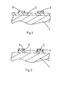
- Figures 1 and 2 are cross-sectional views showing subsequent stages in the formation of a plasma etch resistant mask on a substrate using a method in accordance with the invention.
- the following description relates to the manufacture of a photomask suitable for use in conventional photolithographic techniques employed in semiconductor wafer processing.
- a layer 2 of chromium is deposited, for example using conventional sputtering techniques onto an alumino-silicate or synthetic quartz substrate 1.
- a film of a cross-linked positive acting resist as described in United Kingdom Patent Specifications GB 1,445,345 and GB 1,500,541 is then provided on the chromium layer 2.
- the resist which may, for example, comprise a mixture of poly-(methyl methacrylate-co-methacrylic acid) and poly-(methyl methacrylate-co-methacryloyl chloride) is sensitive to electron radiation so that the resist film can be patterned using electron beam lithography techniques well-known to those skilled in the art.
- the resist film is developed to leave the patterned resist film 3.
- the resist film 3 is exposed to a carbon monoxide plasma at 0.4 Torr, 100W for 5 minutes, in a conventional plasma etching apparatus.
- this treatment forms at the surface of the patterned resist film 3 a region 4 having an enhanced resistance to a subsequent plasma etching step.
- this result is particularly surprising in view of the fact that a similar treatment carried out by the Applicants with other plasmas has not enhanced the etch resistance of the mask and in some cases the etch resistance has even been impaired by such a treatment.
- the next step involves patterning the chromium layer 2 by plasma etching.
- the patterned resist film 3 with the surface region 4 acts to mask the underlying parts of the chromium layer 2. It has been found in practice that the resistance of the plasma etch resistant region 4 can increase the etch resistance of the mask by a factor of two.
- the chromium may be etched in a plasma containing 1 part carbontetrachloride to 1 part oxygen in 3 parts of a carrier gas such as argon or carbon monoxide at 0.5 Torr., 400 watts for 10 minutes.
- the patterned resist film 3 together with region 4 are then removed using fuming nitric acid to leave the photomask comprising the patterned opaque chromium layer 2 on the glass substrate 1.
- a similar method to that described above may also be used to manufacture a photocathode mask for use in the known technique of electron beam image projection.
- the substrate 1 would be made of quartz, but the surface layer 2 would again comprise chromium.
- the patterned chromium layer and the exposed surface parts of the substrate would be coated with a photocathode material, such as caesium iodide, which can act as an electron source when the mask is flooded from behind with ultraviolet radiation.
- a method in accordance with the invention may also be used directly to process a semiconductor wafer.
- the substrate I would itself be the semiconductor wafer and the s rface layer 2 would be a layer of material, for example an oxide, which is capable of masking the semiconductor surface against a subsequent processing step.
Landscapes
- Physics & Mathematics (AREA)
- General Physics & Mathematics (AREA)
- Photosensitive Polymer And Photoresist Processing (AREA)
- Preparing Plates And Mask In Photomechanical Process (AREA)
- ing And Chemical Polishing (AREA)
- Exposure Of Semiconductors, Excluding Electron Or Ion Beam Exposure (AREA)
- Drying Of Semiconductors (AREA)
- Exposure And Positioning Against Photoresist Photosensitive Materials (AREA)
Applications Claiming Priority (2)
| Application Number | Priority Date | Filing Date | Title |
|---|---|---|---|
| GB08215432A GB2121198A (en) | 1982-05-26 | 1982-05-26 | Plasma-etch resistant mask formation |
| GB8215432 | 1982-05-26 |
Publications (3)
| Publication Number | Publication Date |
|---|---|
| EP0095212A2 true EP0095212A2 (fr) | 1983-11-30 |
| EP0095212A3 EP0095212A3 (en) | 1985-01-16 |
| EP0095212B1 EP0095212B1 (fr) | 1988-03-02 |
Family
ID=10530658
Family Applications (1)
| Application Number | Title | Priority Date | Filing Date |
|---|---|---|---|
| EP83200698A Expired EP0095212B1 (fr) | 1982-05-26 | 1983-05-17 | Procédé pour l'obention d'un masque résistant à l'attaque par plasma |
Country Status (5)
| Country | Link |
|---|---|
| US (1) | US4504574A (fr) |
| EP (1) | EP0095212B1 (fr) |
| JP (1) | JPS59154A (fr) |
| DE (1) | DE3375839D1 (fr) |
| GB (1) | GB2121198A (fr) |
Families Citing this family (23)
| Publication number | Priority date | Publication date | Assignee | Title |
|---|---|---|---|---|
| GB2121197A (en) * | 1982-05-26 | 1983-12-14 | Philips Electronic Associated | Plasma-etch resistant mask formation |
| US4601778A (en) * | 1985-02-25 | 1986-07-22 | Motorola, Inc. | Maskless etching of polysilicon |
| EP0238690B1 (fr) * | 1986-03-27 | 1991-11-06 | International Business Machines Corporation | Procédé pour la formation de flancs latéraux |
| JP2550982B2 (ja) * | 1987-04-06 | 1996-11-06 | 富士通株式会社 | レジストマスクの形成方法 |
| US5545290A (en) * | 1987-07-09 | 1996-08-13 | Texas Instruments Incorporated | Etching method |
| US4873176A (en) * | 1987-08-28 | 1989-10-10 | Shipley Company Inc. | Reticulation resistant photoresist coating |
| US5912187A (en) * | 1993-12-30 | 1999-06-15 | Lucent Technologies Inc. | Method of fabricating circuits |
| WO2001018859A1 (fr) | 1999-09-10 | 2001-03-15 | Unaxis Usa Inc. | Dispositif et procede de fabrication d'un pole magnetique |
| US6547975B1 (en) | 1999-10-29 | 2003-04-15 | Unaxis Usa Inc. | Magnetic pole fabrication process and device |
| US20030003374A1 (en) * | 2001-06-15 | 2003-01-02 | Applied Materials, Inc. | Etch process for photolithographic reticle manufacturing with improved etch bias |
| US7183201B2 (en) | 2001-07-23 | 2007-02-27 | Applied Materials, Inc. | Selective etching of organosilicate films over silicon oxide stop etch layers |
| WO2003021659A1 (fr) | 2001-09-04 | 2003-03-13 | Applied Materials, Inc. | Procedes et appareils pour la gravure de couches metalliques sur des substrats |
| WO2003089990A2 (fr) * | 2002-04-19 | 2003-10-30 | Applied Materials, Inc. | Procede de gravure d'une chambre |
| WO2004086143A2 (fr) * | 2003-03-21 | 2004-10-07 | Applied Materials, Inc. | Procede a plusieurs etapes permettant d'attaquer chimiquement des photomasques |
| US20040192058A1 (en) * | 2003-03-28 | 2004-09-30 | Taiwan Semiconductor Manufacturing Co., Ltd. | Pre-etching plasma treatment to form dual damascene with improved profile |
| US7077973B2 (en) * | 2003-04-18 | 2006-07-18 | Applied Materials, Inc. | Methods for substrate orientation |
| KR100630677B1 (ko) * | 2003-07-02 | 2006-10-02 | 삼성전자주식회사 | 포토레지스트 패턴에의 불소를 포함하지 않는 탄소 함유폴리머 생성을 위한 플라즈마 전처리를 포함하는 식각 방법 |
| US7521000B2 (en) * | 2003-08-28 | 2009-04-21 | Applied Materials, Inc. | Process for etching photomasks |
| US8293430B2 (en) * | 2005-01-27 | 2012-10-23 | Applied Materials, Inc. | Method for etching a molybdenum layer suitable for photomask fabrication |
| US7829243B2 (en) * | 2005-01-27 | 2010-11-09 | Applied Materials, Inc. | Method for plasma etching a chromium layer suitable for photomask fabrication |
| CN101046626B (zh) * | 2006-03-30 | 2012-03-14 | 应用材料公司 | 适于制造光掩模的蚀刻钼层方法 |
| KR100944846B1 (ko) * | 2006-10-30 | 2010-03-04 | 어플라이드 머티어리얼스, 인코포레이티드 | 마스크 에칭 프로세스 |
| US8507191B2 (en) | 2011-01-07 | 2013-08-13 | Micron Technology, Inc. | Methods of forming a patterned, silicon-enriched developable antireflective material and semiconductor device structures including the same |
Family Cites Families (6)
| Publication number | Priority date | Publication date | Assignee | Title |
|---|---|---|---|---|
| US4253888A (en) * | 1978-06-16 | 1981-03-03 | Matsushita Electric Industrial Co., Ltd. | Pretreatment of photoresist masking layers resulting in higher temperature device processing |
| US4187331A (en) * | 1978-08-24 | 1980-02-05 | International Business Machines Corp. | Fluorine plasma resist image hardening |
| NL8004007A (nl) * | 1980-07-11 | 1982-02-01 | Philips Nv | Werkwijze voor het vervaardigen van een halfgeleider- inrichting. |
| US4382985A (en) * | 1980-10-11 | 1983-05-10 | Daikin Kogyo Co., Ltd. | Process for forming film of fluoroalkyl acrylate polymer on substrate and process for preparing patterned resist from the film |
| US4370405A (en) * | 1981-03-30 | 1983-01-25 | Hewlett-Packard Company | Multilayer photoresist process utilizing an absorbant dye |
| US4373018A (en) * | 1981-06-05 | 1983-02-08 | Bell Telephone Laboratories, Incorporated | Multiple exposure microlithography patterning method |
-
1982
- 1982-05-26 GB GB08215432A patent/GB2121198A/en not_active Withdrawn
-
1983
- 1983-05-17 EP EP83200698A patent/EP0095212B1/fr not_active Expired
- 1983-05-17 DE DE8383200698T patent/DE3375839D1/de not_active Expired
- 1983-05-20 US US06/496,702 patent/US4504574A/en not_active Expired - Fee Related
- 1983-05-23 JP JP58089308A patent/JPS59154A/ja active Granted
Also Published As
| Publication number | Publication date |
|---|---|
| EP0095212B1 (fr) | 1988-03-02 |
| GB2121198A (en) | 1983-12-14 |
| JPH0261736B2 (fr) | 1990-12-20 |
| DE3375839D1 (en) | 1988-04-07 |
| EP0095212A3 (en) | 1985-01-16 |
| JPS59154A (ja) | 1984-01-05 |
| US4504574A (en) | 1985-03-12 |
Similar Documents
| Publication | Publication Date | Title |
|---|---|---|
| US4504574A (en) | Method of forming a resist mask resistant to plasma etching | |
| US4600686A (en) | Method of forming a resist mask resistant to plasma etching | |
| US5948570A (en) | Process for dry lithographic etching | |
| US4717625A (en) | Photomask material | |
| EP0195291B1 (fr) | Procédé pour obtenir des surfaces texturées dans des films multicouches et emploi dans la fabrication de circuits et systèmes semi-conducteurs | |
| JPS5949536A (ja) | 微細パタ−ン形成方法 | |
| EP0021719B1 (fr) | Procédé pour la fabrication d'images résistantes négatives et images résistantes | |
| US4101782A (en) | Process for making patterns in resist and for making ion absorption masks useful therewith | |
| JP2867479B2 (ja) | レジストパターンの形成方法 | |
| US4268607A (en) | Method of patterning a resist layer for manufacture of a semiconductor element | |
| EP0104235A4 (fr) | Procede de formation d'un materiau de protection lithographique hybride a rayon electronique/optique. | |
| JPH0290170A (ja) | パターン形成方法 | |
| EP0077057B2 (fr) | Réserve de type négatif sensible aux rayons ionisants | |
| JPH0381143B2 (fr) | ||
| JPS5836494B2 (ja) | シヤシンシヨツコクヨウホト マスクノセイゾウホウホウ | |
| US4954424A (en) | Pattern fabrication by radiation-induced graft copolymerization | |
| JPS58105142A (ja) | 遠紫外線感応性レジスト材料及びその使用方法 | |
| KR100442968B1 (ko) | 반도체소자의감광막형성방법 | |
| JPS61173245A (ja) | ホトレジストパタ−ンの形成方法 | |
| CA1075523A (fr) | Methode de conversion d'une couche photoresistante positive en image photoresistante negative | |
| JPS58153334A (ja) | クロム系膜のドライエツチング法 | |
| JPH03269533A (ja) | フォトマスクの製造方法およびそれに使用する基板 | |
| JPH05281702A (ja) | 位相シフトマスクの製造方法 | |
| JPS6160574B2 (fr) | ||
| JPS61248048A (ja) | パタ−ン転写用マスク |
Legal Events
| Date | Code | Title | Description |
|---|---|---|---|
| PUAI | Public reference made under article 153(3) epc to a published international application that has entered the european phase |
Free format text: ORIGINAL CODE: 0009012 |
|
| AK | Designated contracting states |
Designated state(s): DE FR GB NL |
|
| PUAL | Search report despatched |
Free format text: ORIGINAL CODE: 0009013 |
|
| AK | Designated contracting states |
Designated state(s): DE FR GB NL |
|
| 17P | Request for examination filed |
Effective date: 19850312 |
|
| 17Q | First examination report despatched |
Effective date: 19860820 |
|
| GRAA | (expected) grant |
Free format text: ORIGINAL CODE: 0009210 |
|
| AK | Designated contracting states |
Kind code of ref document: B1 Designated state(s): DE FR GB NL |
|
| REF | Corresponds to: |
Ref document number: 3375839 Country of ref document: DE Date of ref document: 19880407 |
|
| ET | Fr: translation filed | ||
| RAP4 | Party data changed (patent owner data changed or rights of a patent transferred) |
Owner name: N.V. PHILIPS' GLOEILAMPENFABRIEKEN Owner name: PHILIPS ELECTRONIC AND ASSOCIATED INDUSTRIES LIMIT |
|
| PLBE | No opposition filed within time limit |
Free format text: ORIGINAL CODE: 0009261 |
|
| STAA | Information on the status of an ep patent application or granted ep patent |
Free format text: STATUS: NO OPPOSITION FILED WITHIN TIME LIMIT |
|
| 26N | No opposition filed | ||
| PGFP | Annual fee paid to national office [announced via postgrant information from national office to epo] |
Ref country code: NL Payment date: 19900531 Year of fee payment: 8 |
|
| PGFP | Annual fee paid to national office [announced via postgrant information from national office to epo] |
Ref country code: GB Payment date: 19910501 Year of fee payment: 9 |
|
| PGFP | Annual fee paid to national office [announced via postgrant information from national office to epo] |
Ref country code: FR Payment date: 19910522 Year of fee payment: 9 |
|
| PGFP | Annual fee paid to national office [announced via postgrant information from national office to epo] |
Ref country code: DE Payment date: 19910726 Year of fee payment: 9 |
|
| PG25 | Lapsed in a contracting state [announced via postgrant information from national office to epo] |
Ref country code: NL Effective date: 19911201 |
|
| NLV4 | Nl: lapsed or anulled due to non-payment of the annual fee | ||
| PG25 | Lapsed in a contracting state [announced via postgrant information from national office to epo] |
Ref country code: GB Effective date: 19920517 |
|
| GBPC | Gb: european patent ceased through non-payment of renewal fee |
Effective date: 19920517 |
|
| PG25 | Lapsed in a contracting state [announced via postgrant information from national office to epo] |
Ref country code: FR Effective date: 19930129 |
|
| PG25 | Lapsed in a contracting state [announced via postgrant information from national office to epo] |
Ref country code: DE Effective date: 19930202 |
|
| REG | Reference to a national code |
Ref country code: FR Ref legal event code: ST |