EP0095389B1 - Datenübertragungssystem - Google Patents
Datenübertragungssystem Download PDFInfo
- Publication number
- EP0095389B1 EP0095389B1 EP83303030A EP83303030A EP0095389B1 EP 0095389 B1 EP0095389 B1 EP 0095389B1 EP 83303030 A EP83303030 A EP 83303030A EP 83303030 A EP83303030 A EP 83303030A EP 0095389 B1 EP0095389 B1 EP 0095389B1
- Authority
- EP
- European Patent Office
- Prior art keywords
- signal
- data
- transmission system
- data transmission
- monitoring
- Prior art date
- Legal status (The legal status is an assumption and is not a legal conclusion. Google has not performed a legal analysis and makes no representation as to the accuracy of the status listed.)
- Expired
Links
Images


Classifications
-
- H—ELECTRICITY
- H04—ELECTRIC COMMUNICATION TECHNIQUE
- H04L—TRANSMISSION OF DIGITAL INFORMATION, e.g. TELEGRAPHIC COMMUNICATION
- H04L12/00—Data switching networks
- H04L12/28—Data switching networks characterised by path configuration, e.g. LAN [Local Area Networks] or WAN [Wide Area Networks]
- H04L12/40—Bus networks
- H04L12/407—Bus networks with decentralised control
- H04L12/413—Bus networks with decentralised control with random access, e.g. carrier-sense multiple-access with collision detection [CSMA-CD]
-
- H—ELECTRICITY
- H04—ELECTRIC COMMUNICATION TECHNIQUE
- H04L—TRANSMISSION OF DIGITAL INFORMATION, e.g. TELEGRAPHIC COMMUNICATION
- H04L1/00—Arrangements for detecting or preventing errors in the information received
- H04L1/20—Arrangements for detecting or preventing errors in the information received using signal quality detector
-
- H—ELECTRICITY
- H04—ELECTRIC COMMUNICATION TECHNIQUE
- H04L—TRANSMISSION OF DIGITAL INFORMATION, e.g. TELEGRAPHIC COMMUNICATION
- H04L12/00—Data switching networks
- H04L12/28—Data switching networks characterised by path configuration, e.g. LAN [Local Area Networks] or WAN [Wide Area Networks]
- H04L12/40—Bus networks
Definitions
- This invention relates to a data transmission system wherein a plurality of transmitters are connected to a common communication channel in a multidrop manner.
- Fig. 1 A typical example of a multidrop connection scheme is illustrated in Fig. 1, which includes a power distribution cable 1 and a plurality of transmission modules 2 for transmission and reception of data.
- Fig. 1 A typical example of a multidrop connection scheme is illustrated in Fig. 1, which includes a power distribution cable 1 and a plurality of transmission modules 2 for transmission and reception of data.
- the most serious problem in this kind of system is that in the event that any one of the transmission modules 2 is faulty in a hardware aspect but signals representative of transmission data are supplied continuously to the cable 1 the system becomes disabled as a whole and fails to send signals. If a large number of modules are installed, it is very difficult to determine which module is faulty.
- US-A-4063220 discloses a data communication system in which a number of transceivers, each forming part of a respective communication station are interconnected via a communication network, e.g. a coaxial cable.
- Each transceiver also includes a collision detector to determine whether or not, when signals are transmitted onto the network from that station, the network is already busy.
- the transmitter stage of the transceiver is disconnected from the communication network in the event that either one of two transistors through which data signals are coupled to the cable is ON for an excessive period.
- the data coupled on to the line may be in Manchester code format.
- This known system does not include complete protection from a faulty station. Only when one of the transistors is ON for too long will disconnection take place, and there is no recognition of the possibility of failure being indicated by an excessively long transistor OFF period.
- a data transmission system comprising a plurality of data transmitters (2) having a common communication channel (1), each transmitter being arranged to transmit data in a coded format such that transitions between a plurality of signal levels occur at least once in every predetermined interval, each transmitter having means (22, 27, 28) for monitoring its transmission and for inhibiting such a transmission if, while the transmitter is transmitting the data signal remains at a said signal level for longer than a predetermined time, characterised in that said monitoring means (22, 27, 28) is arranged to monitor the periods that the data signal remains at each of said signal levels and to inhibit the transmission if any of said periods exceeds said predetermined time.
- the coded format is the Manchester code, and data to be transmitted is converted into said Manchester code from a NRZ (Non Return to Zero) code. Also, the predetermined time is longer than the predetermined interval, which is the bit interval.
- the simplest data format is a so-called NRZ (Non Return to Zero) in which the signal level corresponds to the data on a one-to-one basis.
- NRZ Non Return to Zero
- a voltage corresponding to the data is applied to a signal line at each predetermined time interval T as seen in Fig. 2.
- a data "1" is defined by a voltage Vp and a data "0" by a voltage V M , but if the same data is transmitted continuously in the NRZ notation, the level remains constant and unchanged. This makes it very difficult to distinguish between correct data transmission and hardware failure in the system.
- the above problem can be overcome, provided that data are not represented by voltage levels on the one-to-one basis but by voltage level transitions.
- each bit time T is divided into two half slots and a data "0" is defined by a combination of levels “1” and “0” in time sequence and a data "1” by a combination of levels “0” and “1” in time sequence (or vice versa).
- a data "0" is defined by a combination of levels “1” and “0” in time sequence
- a data "1” by a combination of levels "0” and “1” in time sequence (or vice versa).
- Fig. 4 In normal operation there is never a signal portion lasting at the same level for more than T seconds for possible four combinations of data, as will be understood from Fig. 4.
- any signal lasts at the same level for more than T seconds in the above code system, it can be assumed that a hardware fault has occurred somewhere in the system, as long as such erroneous signal is distinguished from a silence.
- a reference time is selected to be longer than T and preferably selected to be more than 2 ⁇ . If there is no variation in the level of the signal being transmitted for more than such reference time, then the remedy taken thereafter is to treat the subject transmission module as having a hardware problem, disconnect its level supplying section and indicate that the subject module is out of condition.
- a cable 1 for module- to-module signal transmission (also for power distribution), a disconnecting switch, 21 for disconnecting the transmission module or modules from the transmission cable during a silence interval and for forced interruption of transmission upon fault detection and an AND gate 24 for controlling the switch 21.
- a transmission output section is denoted by 22 and whether the output section 22 is in the transmission state is determined by a signal TXSENSE.
- a transmission level setting section 23 outputs levels corresponding to outputs from the preceding code converter 25.
- the code converter 25 is adapted to convert NRZ data into a suitable code notation (the Manchester code or the like as described above).
- a data generation and control section 26 on one hand feeds the NRZ data to the code converter 25 and on the other hand feeds a transmission/disconnection signal TXENABLE to the AND gate 24.
- Another AND gate 27 is to permit monitoring of the transmission level by the signal TXSENSE only while the switch 21 is ON.
- a timer 28 is adapted for measuring the time for which the signal remains at the same level, and more particularly is cleared at every level transition and continuous time counting while the transmission level remains unchanged.
- the data generation and control section 26 When the reference time is reached by the timer, its output TIMEOUT becomes true so that the output of the AND gate 24 is false and the switch 21 is turned OFF to force transmission to stop.
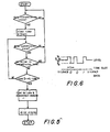
- the data generation and control section 26 Since the data generation and control section 26 is usually implemented with a microcomputer or complicated hardware logic connection, this section more often causes a hardware trouble than the other sections in Fig. 7. In particular, when this is implemented with the microcomputer, it demands a special means to recover after a program sequence therein falls into disorder and the section gets out of control. To this end the signal TIMEOUT is applied as a RESET signal to the data generation and control section 26, with concurrent inhibition of level supply. Should the data control section return to its normal state with the signal RESET, the system is ready to re-start transmission. Unless the data control section recovers its normal state, the subject module is disabled to supply the level and the system is disabled to transmit data to and from that module. However, there is never complete breakdown of the system.
- the signal TXSENSE is derived from an OR gate 34 responsive to the outputs of the two detector circuits 32 and 33.
- the detection levels may be optionally selected through the use of R S1 and R S2 with the resistances determined by the following definition.
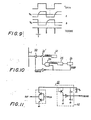
- FIG. 9 Various signals occurring in the circuit of Fig. 8 in operation are depicted in Fig. 9.
- the output of the circuit 32 is A and the output of the circuit 33 is B.
- Charging of a capacitor C via a resistor R starts when a transistor T 3 orT 4 in the detector circuits is turned ON and the output appears with a time delay T determined as a function of the CR time constant and the threshold voltage Vth of the OR gate 34 as follows:
- the timer 28 of Fig. 7 is made up by a CR integration circuit. Whenever the level of the signal under transmission changes, the signal TXSENSE never fail to fall to zero for the time T. This results in initializing the timer to zero and re-starting time measurement. As already described, if the signal TXSENSE lasts for more than the reference time, the signal TIMEOUT is developed to force the transmission state to a halt.
- FIG. 10 Another embodiment of the present invention using AM modulation is shown in Fig. 10, with simpler circuit than the previous embodiment of Fig. 7.
- the components 1, 22, 24-26 are similar to those in Fig. 7.
- a transmission/disconnection switch 21 also serves to determine whether to apply the carrier.
- a carrier oscillator is denoted by 41.
- Fig. 11 shows a circuit corresponding to that in Fig. 8, wherein a CR integration circuit 42 is equivalent to the timer 28 of Fig. 7.
- the CR time constant of the integration circuit 42 is selected within a range from T to 2 T .
- the circuit 33 in Fig. 8 is not necessary because of the need for only decision as to whether to apply the carrier.
Landscapes
- Engineering & Computer Science (AREA)
- Computer Networks & Wireless Communication (AREA)
- Signal Processing (AREA)
- Quality & Reliability (AREA)
- Dc Digital Transmission (AREA)
- Small-Scale Networks (AREA)
Claims (10)
Applications Claiming Priority (2)
| Application Number | Priority Date | Filing Date | Title |
|---|---|---|---|
| JP57089251A JPS58205353A (ja) | 1982-05-25 | 1982-05-25 | デ−タ伝送システム |
| JP89251/82 | 1982-05-25 |
Publications (3)
| Publication Number | Publication Date |
|---|---|
| EP0095389A2 EP0095389A2 (de) | 1983-11-30 |
| EP0095389A3 EP0095389A3 (en) | 1985-05-15 |
| EP0095389B1 true EP0095389B1 (de) | 1988-05-11 |
Family
ID=13965535
Family Applications (1)
| Application Number | Title | Priority Date | Filing Date |
|---|---|---|---|
| EP83303030A Expired EP0095389B1 (de) | 1982-05-25 | 1983-05-25 | Datenübertragungssystem |
Country Status (5)
| Country | Link |
|---|---|
| US (1) | US4888586A (de) |
| EP (1) | EP0095389B1 (de) |
| JP (1) | JPS58205353A (de) |
| CA (1) | CA1194954A (de) |
| DE (1) | DE3376611D1 (de) |
Families Citing this family (11)
| Publication number | Priority date | Publication date | Assignee | Title |
|---|---|---|---|---|
| US5266943A (en) * | 1982-05-25 | 1993-11-30 | Sharp Kabushiki Kaisha | Data transmission system |
| US5142530A (en) * | 1989-10-16 | 1992-08-25 | International Business Machines Corporation | Multi-frame stripping protocol for token ring networks |
| DE4034916A1 (de) * | 1990-11-01 | 1992-05-07 | Siemens Ag | Aktiver stern fuer ein optisches uebertragungssystem |
| DE69132259T2 (de) * | 1990-12-04 | 2000-10-26 | The Furukawa Electric Co., Ltd. | Vorrichtung zur spannungseinstellung in einem multiplexübertragungssystem |
| JP2639373B2 (ja) * | 1995-01-17 | 1997-08-13 | 株式会社ニコン | カメラシステム、カメラ及びそのアクセサリー |
| FR2769780B1 (fr) * | 1997-10-10 | 2000-01-28 | Peugeot | Systeme de transmission d'informations entre stations raccordees par un reseau multiplexe, notamment pour vehicule automobile |
| US6865181B1 (en) | 1999-03-22 | 2005-03-08 | Cisco Technology, Inc. | Method and apparatus for routing telecommunications signals |
| US7924706B1 (en) | 1999-03-22 | 2011-04-12 | Cisco Technology, Inc. | Method and apparatus for controlling the operation of a flexible cross-connect system |
| US7035204B1 (en) | 2000-07-26 | 2006-04-25 | Cicso Technology, Inc. | Method and apparatus for rerouting telecommunications signals |
| US7929448B2 (en) * | 2006-10-17 | 2011-04-19 | Verizon Patent And Licensing Inc. | Monitoring link aggregation links |
| US7835291B2 (en) * | 2006-10-17 | 2010-11-16 | Verizon Patent And Licensing Inc. | Disabled state and state signaling for link aggregation |
Family Cites Families (6)
| Publication number | Priority date | Publication date | Assignee | Title |
|---|---|---|---|---|
| JPS5432283B2 (de) * | 1973-08-27 | 1979-10-13 | ||
| US4063220A (en) * | 1975-03-31 | 1977-12-13 | Xerox Corporation | Multipoint data communication system with collision detection |
| JPS55117362A (en) * | 1979-03-02 | 1980-09-09 | Nec Corp | Input break detection circuit for cmi code |
| JPS5811784B2 (ja) * | 1979-10-03 | 1983-03-04 | 株式会社日立製作所 | デイジタル信号伝送装置の異常検出方式 |
| GB2094110A (en) * | 1981-01-30 | 1982-09-08 | Eltra Corp | A method and apparatus for locating a discontinuity in a data transmission |
| US4561091A (en) * | 1983-09-23 | 1985-12-24 | Codenoll Technology Corporation | Data receiver |
-
1982
- 1982-05-25 JP JP57089251A patent/JPS58205353A/ja active Pending
-
1983
- 1983-05-25 CA CA000428881A patent/CA1194954A/en not_active Expired
- 1983-05-25 DE DE8383303030T patent/DE3376611D1/de not_active Expired
- 1983-05-25 US US06/498,052 patent/US4888586A/en not_active Expired - Fee Related
- 1983-05-25 EP EP83303030A patent/EP0095389B1/de not_active Expired
Also Published As
| Publication number | Publication date |
|---|---|
| CA1194954A (en) | 1985-10-08 |
| DE3376611D1 (en) | 1988-06-16 |
| US4888586A (en) | 1989-12-19 |
| EP0095389A3 (en) | 1985-05-15 |
| JPS58205353A (ja) | 1983-11-30 |
| EP0095389A2 (de) | 1983-11-30 |
Similar Documents
| Publication | Publication Date | Title |
|---|---|---|
| US6011821A (en) | Process for synchronization of matching circuits of a communication system with several modules | |
| EP0095389B1 (de) | Datenübertragungssystem | |
| US6396282B1 (en) | Process for testing the ground contact of parts of a networked system | |
| KR0138266B1 (ko) | 전력제어시스템의 장치간에 절연을 제공하고 그 절연수단을 통해 전력 및 데이타를 전송하기 위한 회로 | |
| US4580295A (en) | System for monitoring optical data bus transmissions | |
| US5161151A (en) | System and method for controlling multiplex communications between master station and slave stations | |
| US4257033A (en) | Fault locating system in optical fiber transmission system | |
| CA1155194A (en) | Optically coupled serial communication bus | |
| US4187415A (en) | Remote locating system for transmission faults in data transmission line having regenerative repeaters | |
| US5483639A (en) | Device for detecting transmission errors in balanced two-wire bus lines and two-bus interfaces | |
| EP0033932B1 (de) | Kombinierte Überwachung und Fehlerortung in Übertragungsstrecken für digitale Signale | |
| GB2058418A (en) | A multiplex information handling system | |
| US6453432B1 (en) | Method and system for communicating the status of a digital transmission line element during loopback | |
| US5266943A (en) | Data transmission system | |
| US4680431A (en) | Data network interface module with circuitry for disconnecting a module that has lost supply voltage | |
| US4355215A (en) | Remote control systems for telecommunications links | |
| US4446550A (en) | Reliable signal system having at least one transmitter feeding plural series-connected receiver inputs | |
| US5473308A (en) | Remote supervisory system for network elements | |
| WO2003032531A2 (en) | Fiber optic conversion system and method | |
| GB2051438A (en) | Security alarm systems | |
| US7421366B2 (en) | Bus station connection to a bus system for restraining means and/or sensors | |
| JPH069071B2 (ja) | 火報システムの中継器 | |
| WO2025134225A1 (ja) | 制御・監視信号伝送システム | |
| JP3014602B2 (ja) | 光伝送システムの伝送路監視方法 | |
| JPS60106233A (ja) | 伝送路切替装置 |
Legal Events
| Date | Code | Title | Description |
|---|---|---|---|
| PUAI | Public reference made under article 153(3) epc to a published international application that has entered the european phase |
Free format text: ORIGINAL CODE: 0009012 |
|
| AK | Designated contracting states |
Designated state(s): DE FR GB IT |
|
| PUAL | Search report despatched |
Free format text: ORIGINAL CODE: 0009013 |
|
| AK | Designated contracting states |
Designated state(s): DE FR GB IT |
|
| 17P | Request for examination filed |
Effective date: 19851021 |
|
| 17Q | First examination report despatched |
Effective date: 19861003 |
|
| ITF | It: translation for a ep patent filed | ||
| GRAA | (expected) grant |
Free format text: ORIGINAL CODE: 0009210 |
|
| AK | Designated contracting states |
Kind code of ref document: B1 Designated state(s): DE FR GB IT |
|
| REF | Corresponds to: |
Ref document number: 3376611 Country of ref document: DE Date of ref document: 19880616 |
|
| ET | Fr: translation filed | ||
| PLBE | No opposition filed within time limit |
Free format text: ORIGINAL CODE: 0009261 |
|
| STAA | Information on the status of an ep patent application or granted ep patent |
Free format text: STATUS: NO OPPOSITION FILED WITHIN TIME LIMIT |
|
| 26N | No opposition filed | ||
| ITTA | It: last paid annual fee | ||
| PGFP | Annual fee paid to national office [announced via postgrant information from national office to epo] |
Ref country code: FR Payment date: 19960510 Year of fee payment: 14 |
|
| PGFP | Annual fee paid to national office [announced via postgrant information from national office to epo] |
Ref country code: GB Payment date: 19960516 Year of fee payment: 14 |
|
| PGFP | Annual fee paid to national office [announced via postgrant information from national office to epo] |
Ref country code: DE Payment date: 19960528 Year of fee payment: 14 |
|
| PG25 | Lapsed in a contracting state [announced via postgrant information from national office to epo] |
Ref country code: GB Effective date: 19970525 |
|
| GBPC | Gb: european patent ceased through non-payment of renewal fee |
Effective date: 19970525 |
|
| PG25 | Lapsed in a contracting state [announced via postgrant information from national office to epo] |
Ref country code: FR Free format text: LAPSE BECAUSE OF NON-PAYMENT OF DUE FEES Effective date: 19980130 |
|
| PG25 | Lapsed in a contracting state [announced via postgrant information from national office to epo] |
Ref country code: DE Free format text: LAPSE BECAUSE OF NON-PAYMENT OF DUE FEES Effective date: 19980203 |
|
| REG | Reference to a national code |
Ref country code: FR Ref legal event code: ST |