EP0096163A2 - Appareil pour diviser les éléments d'un champ de Galois - Google Patents
Appareil pour diviser les éléments d'un champ de Galois Download PDFInfo
- Publication number
- EP0096163A2 EP0096163A2 EP83102173A EP83102173A EP0096163A2 EP 0096163 A2 EP0096163 A2 EP 0096163A2 EP 83102173 A EP83102173 A EP 83102173A EP 83102173 A EP83102173 A EP 83102173A EP 0096163 A2 EP0096163 A2 EP 0096163A2
- Authority
- EP
- European Patent Office
- Prior art keywords
- linear shift
- shift registers
- circuit
- circuits
- gate
- Prior art date
- Legal status (The legal status is an assumption and is not a legal conclusion. Google has not performed a legal analysis and makes no representation as to the accuracy of the status listed.)
- Granted
Links
Images


Classifications
-
- G—PHYSICS
- G06—COMPUTING OR CALCULATING; COUNTING
- G06F—ELECTRIC DIGITAL DATA PROCESSING
- G06F7/00—Methods or arrangements for processing data by operating upon the order or content of the data handled
- G06F7/38—Methods or arrangements for performing computations using exclusively denominational number representation, e.g. using binary, ternary, decimal representation
- G06F7/48—Methods or arrangements for performing computations using exclusively denominational number representation, e.g. using binary, ternary, decimal representation using non-contact-making devices, e.g. tube, solid state device; using unspecified devices
- G06F7/52—Multiplying; Dividing
-
- H—ELECTRICITY
- H03—ELECTRONIC CIRCUITRY
- H03M—CODING; DECODING; CODE CONVERSION IN GENERAL
- H03M13/00—Coding, decoding or code conversion, for error detection or error correction; Coding theory basic assumptions; Coding bounds; Error probability evaluation methods; Channel models; Simulation or testing of codes
- H03M13/03—Error detection or forward error correction by redundancy in data representation, i.e. code words containing more digits than the source words
- H03M13/05—Error detection or forward error correction by redundancy in data representation, i.e. code words containing more digits than the source words using block codes, i.e. a predetermined number of check bits joined to a predetermined number of information bits
- H03M13/13—Linear codes
- H03M13/15—Cyclic codes, i.e. cyclic shifts of codewords produce other codewords, e.g. codes defined by a generator polynomial, Bose-Chaudhuri-Hocquenghem [BCH] codes
-
- G—PHYSICS
- G06—COMPUTING OR CALCULATING; COUNTING
- G06F—ELECTRIC DIGITAL DATA PROCESSING
- G06F11/00—Error detection; Error correction; Monitoring
- G06F11/07—Responding to the occurrence of a fault, e.g. fault tolerance
- G06F11/08—Error detection or correction by redundancy in data representation, e.g. by using checking codes
- G06F11/10—Adding special bits or symbols to the coded information, e.g. parity check, casting out 9's or 11's
-
- G—PHYSICS
- G06—COMPUTING OR CALCULATING; COUNTING
- G06F—ELECTRIC DIGITAL DATA PROCESSING
- G06F7/00—Methods or arrangements for processing data by operating upon the order or content of the data handled
- G06F7/60—Methods or arrangements for performing computations using a digital non-denominational number representation, i.e. number representation without radix; Computing devices using combinations of denominational and non-denominational quantity representations, e.g. using difunction pulse trains, STEELE computers, phase computers
- G06F7/72—Methods or arrangements for performing computations using a digital non-denominational number representation, i.e. number representation without radix; Computing devices using combinations of denominational and non-denominational quantity representations, e.g. using difunction pulse trains, STEELE computers, phase computers using residue arithmetic
- G06F7/724—Finite field arithmetic
- G06F7/726—Inversion; Reciprocal calculation; Division of elements of a finite field
-
- G—PHYSICS
- G11—INFORMATION STORAGE
- G11B—INFORMATION STORAGE BASED ON RELATIVE MOVEMENT BETWEEN RECORD CARRIER AND TRANSDUCER
- G11B20/00—Signal processing not specific to the method of recording or reproducing; Circuits therefor
- G11B20/10—Digital recording or reproducing
- G11B20/18—Error detection or correction; Testing, e.g. of drop-outs
- G11B20/1806—Pulse code modulation systems for audio signals
- G11B20/1809—Pulse code modulation systems for audio signals by interleaving
Definitions
- the present invention relates to an apparatus for dividing the elements of a Galois field, which can effectively serve to decode an error correction code used in an optical DAD (digital audio disk) device using, for example, a CD (compact disk).
- an optical DAD digital audio disk
- CD compact disk
- cross-interleaved Reed Solomon codes are used as error correction codes.
- a cross-interleaved Reed Solomon code is obtained by submitting a Reed Solomon code, which is a BCH code and which is generally regarded as the most effective random error correction code hitherto known, to a signal process called "cross-interleaving".
- the cross-interleaved Reed Solomon code thus obtained can correct even a burst error.
- a Reed Solomon code can be decoded in the same way as is a BCH code, thereby performing an error correction.
- a Reed Solomon code consisting of k data symbols and (n-k) inspection symbols i.e., a code consisting of n symbols
- n symbols are the 2 m elements of a finite field called "Galois field GF(2 m )" which represents m binary bits.
- the generator polynomial g( x ) representing a Reed Solomon code used to correct an error t times is given by the following equation (1) or (2), where a is the origin element of the Galois field GF (2m):
- the coefficients contained in polynomial E(x) are also contained in Galois field GF (2 m ).
- the error polynomial E(x) contains only terms which correspond to an error location and the value (i.e., size) of an error.
- Error location polynomial ⁇ (x) is given by: where e is the number of errors.
- ⁇ 1 to ⁇ e in equation (7) are related to syndrome Si as shown below:
- the Reed Solomon code may decoded in the following method A or the following method B. [Method A]
- Fig. 1 is a block diagram of a known data correcting system which is designed to decode Reed Solomon codes in the manner described above.
- Data to be corrected are supplied through an input terminal IN and will be corrected by a Reed Solomon code.
- the data are stored in a data buffer 11 and kept stored there until a code decoding (later described) is completed.
- the data are supplied also to a syndrome calculator 12.
- the calculator 12 calculates a syndrome based on the input data and the syndrome is then stored in a syndrome buffer 13.
- An OR gate is coupled to the output of the syndrome buffer 13. It generates an output signal which indicates whether or not an error exists in the syndrome supplied from the syndrome buffer 13.
- An output signal from the OR gate is supplied to an error location polynomial calculator 15.
- the calculator 15 finds the coefficients included in an error location polynomial ⁇ ( x ⁇ . Data representing the coefficients are fed to an error location calculator 16.
- the error location calculator 16 finds the root or roots of the error location polynomial. Data representing the root or roots are supplied from the calculator 16 to an error value calculator 17. From the input data the calculator 17 calculates an error value. The data representing the root or roots and the data representing the error value are used to correct the data from the data buffer 11.
- the calculators 12, 15, 16 and 17 of the data correcting system can detect elements which are "0" and can therefore perform algebraic operations such as addition, multiplication or division.
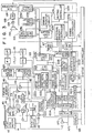
- the error location polynomial calculator 16 may have such a structure as shown in Fig. 2 and disclosed in U.S. Patent No. 4,142,174.
- the error location polynomial calculator 16 comprises a syndrome buffer 21, a working buffer 22, a sequence controller 23, a logarithm buffer 24 and an antilogarithm buffer 25.
- the syndrome buffer 21 is a random-access memory (RAM) for storing a syndrome Si which is m-bit data and which represents each element of a Galois field GF(2 m ).
- the working buffer 22 is a RAM for storing an interim result of an algebraic operation performed in finding the coefficients of the error location polynomial and for storing the final result of the algebraic operation.
- the working buffer 22 may store partial results that will be used in algebraic operations which follow the operations for calculating the coefficients of the error location polynomial.
- the sequence controller 23 defines the order in which algebraic operations will be performed. It supplies address signals to the syndrome buffer 21 and the working buffer 22, to thereby designate desired memory locations of these buffers 21 and 22 and to check and branch the results of algebraic operations so that the results may be used in the next algebraic operations.
- the logarithm buffer 24 is a ROM (read-only memory) storing a table of the logarithms of the elements of a Galois field GF(2 m ).
- the antilogarithm buffer 25 is also a ROM storing a table of the antilogarithms of the elements of a Galois field G F ( 2 m).
- the address of the logarithm buffer 24 is a binary code of element a i . Its entry is the logarithm of a to the base _ that is, i. The entry at address i of the antilogarithm buffer 25 is a binary code of a i .
- eight coefficients a 0 to a 7 may be taken and can be represented as binary vectors. For example, they can be given by:
- the elements of the Galois field GF(2 8 ) other than these can be represented as binary vectors.
- the addresses 1 - 255 of the logarithm table are 8-bit binary vectors of elements a i . Entries corresponding to the addresses are binary notation of exponent i. In the antilogarithm table, exponent i is used as an address, and entries are binary vectors of a i .
- the former is supplied from A register 20 to an exclusive OR gate 27 and the latter is supplied from B register 26 to the exclusive OR gate 27.
- An exclusive logical sum of each bit of element a i and the corresponding bit of element aj is thus produced.
- the logical sum of elements a i and aj obtained by the exclusive OR gate 27 is transferred through C register 19 to the working buffer 22.
- the error location polynomial calculator of the known error correcting system must be provided with a logarithm buffer and an antilogarithm buffer. Without these buffers, the error location polynomial calculator could not perform multiplication or division. Both buffers, which are ROMs, need to have an enormously large memory capacity. This makes it difficult to manufacture the error location polynomial calculator in the form of an LSI. In order to make the calculator in the form of an LSI, the logarithm buffer and the antilogarithm buffer must be excluded from the calculator. In this case, the buffers having a large memory capacity have to be connected to the calculator.
- the known error location polynomial calculator is provided with two ROMs the total memory capacity of which amounts to 4080 bits.
- One of the ROMs stores a table of logarithms and the other ROM stores a table of antilogarithms. Since its error location polynomial calculator has two ROMs both with a large memory capacity, the error correcting system is inevitably complicated, and thus expensive.
- An object of the present invention is to provide an apparatus for dividing the elements of a Galois field, which has neither a logarithm buffer nor an antilogarithm buffer, both of which require a large memory capacity, and which therefore has a simple structure and can be manufactured at low cost.
- An apparatus divides one element a i of the Galois field GF(2 m ) by another element aj of the Galois field GF(2 m ), where a is a root of modulus polynomial F (x) .
- Data representing element aj are supplied to one of the first linear shift registers through a data line and to the other first linear shift registers through data lines and then through a Nl , a N2 ... multiplier circuits (1 ⁇ N1 ⁇ N2, .
- Data representing a i are supplied to one of the first linear shift registers through a data line and to the other first linear shift registers through data lines and then through other a N l, a N2, ... multiplier circuits (1 ⁇ N1 ⁇ N2, ).
- a plurality of "1" detector circuits are connected to the outputs of the first linear shift registers, respectively, to detect whether or not the outputs from the first linear shift registers represent "1". Until any one of the "1" detector circuits detects "1", the first linear shift registers and the second linear shift registers are shifted several times by shift means.
- a plurality of 2-input gate circuits are connected at one input to the outputs of the "1" detector circuits, respectively, and at the other input to the outputs of the second linear shift registers, respectively.
- the output data from the second linear shift register which corresponds to the first linear shift register connected to the "1" detector circuit which detects.”l" are delivered through output means as data representing the quotient of the division.
- the elements of the Galois field GF(2 m ) are divided by using linear shift registers. More precisely, the linear shift registers are used to multiply the elements of the Galois field GF(2 m ) and ulimately, to divide the elements of the Galois field GF(2 m ). Both dividend a i and divider aj are multiplied by a a proper number of times before the data representing them are supplied to the linear shift registers, and so the linear shift registers need to be shifted fewer times than otherwise, thus performing multiplication (and ultimately, division) in a shorter time.
- the optical DAD device comprises a motor 111 for rotating a turntable 112.
- an optical disk 113 is mounted on the turntable 112 on the turntable 112 .
- the disk 113 has pits which correspond to digital audio signals (i.e. PCM codes) which have been EFM-modulated and interleaved.
- An optical pickup 114 emits a laser beam from a semiconductor laser 114a.
- the laser beam passes through a beam splitter 114b and is focused by an objective lens 114c.
- the beam illuminates the track of the optical disk 113, i.e., a train of pits which cause an interference between an incident laser beam and a reflected laser beam in various ways.
- the beam reflected from the pits passes through the objective lens 114c and the beam splitter 114b.
- the photodetector 114d converts the laser beam into four signals.
- the pickup 114 is moved by a pickup feed motor 115 in the radial direction of the optical disk 113.
- the four signals from the photodetector 114d are supplied to a matrix circuit 116 and undergo a specific matrix operation.
- the matrix circuit l16 generates a focus error signal F, a tracking error signal T and a high-frequency signal RF.
- the focus error signal F and a focus search signal from a focus search circuit 110 drive a focus servo system of the optical pickup 114.
- the tracking error signal T and search control signal from a system controller 117 drive a tracking servo system of the pickup l14 and control the pickup feed motor 115.
- the high-frequency signal RF is supplied to a reproduced signal processing system 118 as a major reproduced signal component.
- the signal RF is supplied to a waveform shaping circuit 120 which is controlled by a slice level (eye pattern) detector 119.
- the waveform shaping circuit 120 divides the input signal into an unnecessary analog component and a necessary data component.
- the necessary data component is supplied to a sync clock reproducing circuit 121 of PLL type and also to an edge detector 112a of a first signal processing system 122.
- a sync clock from the sync clock reproducing circuit 212 is supplied to a clock pulse generating circuit 122.
- the clock pulse generating circuit 122b In response to the sync clock, the clock pulse generating circuit 122b generates a clock pulse for dividing a sync signal into components.
- the necessary data component from the edge detector 122a is supplied to a sync signal detector 122c.
- the sync signal detector 122c divides the data components in response to a sync signal dividing clock pulse from the clock pulse generating circuit 122b.
- the necessary data component from the edge detector 122a is also supplied to a demodulating circuit 122d and then EFM-demodulated.
- a sync signal from the sync signal detector 122c is supplied to a sync signal protecting circuit 122e and then to a timing signal generating circuit 122f.
- a clock pulse signal from the clock pulse generating circuit 122b is also supplied to the timing signal generating circuit 122f.
- the timing signal generating circuit 122f generates a timing signal for processing input data.
- An output signal from the demodulating circuit 122d is supplied through a data bus input/output control circuit 122g to an input/output control circuit 123a of a second signal processing system 123.
- the output signal from the demodulating circuit 122d contains a sub-code (i.e., a control signal) and a display signal component.
- the display signal component is supplied to a sub-code processing circuit 122i.
- the sub-code processing circuit 122i detects an error, if any, from the sub-code and corrects the error and then generates sub-code data.
- the sub-code data is supplied to the system controller 117 through an interface circuit 122q which is connected to the system controller 117.
- the system controller 117 includes a microcomputer, an interface circuit and a driver integrated circuit. In response to an instruction from a control switch 124 the system controller 117 controls the DAD device in a desired manner and causes a display device 125 to display the sub-code, e.g., index data about a piece of music to be reproduced.
- a control switch 124 the system controller 117 controls the DAD device in a desired manner and causes a display device 125 to display the sub-code, e.g., index data about a piece of music to be reproduced.
- a timing signal from the timing signal generating circuit 122f is supplied through a data selecting circuit 122j to the data bus input/output control circuit 122g and controls the data bus input/output control circuit 122g.
- the timing signal is supplied also to a frequency detector 122k and a phase detector 1221 and farther to a PWM modulator 122m.
- the timing signal from the PWM modulator 122m then undergoes automatic frequency control (AFC) and automatic phase control (APC) so as to rotate the motor 111 at a constant linear velocity (CLV).
- AFC automatic frequency control
- API automatic phase control
- the phase detector 1121 is connected to receive a system clock pulse from a system clock pulse generating circuit 122p, which operates under the control of an output signal from a quartz crystal oscillator 122n.
- the demodulated data from the input/output control circuit 123a of the second signal processing system 123 is supplied through a data output circuit 123e to a D/A (digital-to-analog) converter 126 after it has undergone necessary error correction, de-interleaving and data supplementation at a syndrome detector 123b, and an error pointer control circuit 123c and error correction circuit 123d.
- the second signal processing system 123 includes an external memory control circuit 123f.
- the control circuit 123f cooperates with the data selecting circuit 122j of the first signal processing system 122 to control a memory circuit 127 which is provided outside the system 123 and which stores data necessary for correcting errors. Under the control of the circuits 123f and 122j the data are read from the external memory 127 and supplied to the input/output control circuit 123a.
- the second signal processing system 123 further comprises a timing control circuit 123g and a muting control circuit 123h.
- the timing control circuit 123g is so designed as to supply, in response to a system clock pulse from the system clock pulse generating circuit 122p, a timing control signal which is necessary for correcting errors, supplementing data and converting digital data into analog data.
- the muting control circuit 123h is designed to operate in response to a control signal from the error pointer control circuit 123c or from the system controller 117, thus performing a specific muting control which is necessary in supplementing data and in starting and ending DAD reproduction.
- An audio signal, or an analog output signal from the D/A converter 126 is supplied through a low-pass filter 128 and an amplifier 129 to a loudspeaker 130.
- Fig. 4 shows an error location polynomial calculator provided in the error correcting circuit 123d of the second signal processing system 123.
- the calculator is identical to the conventional calculator shown in Fig. 2, except that it is provided with a multiplier 41 and a divider 42 which multiply and divide the elements of a Galois field.
- the apparatus of the invention can therefore divide the elements of a Galois field, although it has neither a logarithm buffer nor an antilogarithm buffer.
- the function of the error location polynomial calculator is to perform various algebraic operations and thereby to decode an error correction code, i.e., a Reed Solomon code which is a BCH code.
- the calculator performs addition and detection of element "0" in the same way as the calculator shown in Fig. 2. It performs multiplication and division in different ways, however. How the calculator achieves multiplication and division will be described below in detail.
- Element a i of Galois field GF(2 8 ), for example, is multiplied by element aj of the Galois field GF(2 8 ), where a is the root of a modulus polynomial F (x) X 8 + X6 + X 5 + X 4 + 1.
- a i and aj be given as follows: where c 0 - c 7 and d 0 - d 7 are each either 1 or 0. Then:
- the multiplier shown in Fig. 5 comprises AND gates AND 0 to AND 7 .
- the coefficients d 0 to d 7 of the multiplier D(a) are supplied to the multiplier one after another. More specifically, the least significant bit d 7 is first supplied to one input of the AND gate AND O , the second least significant bit a 6 is then supplied to one input of the AND gate AND O while the bit d 7 is supplied to one input of the AND gate AND 1 , the third least significant bit a 5 is supplied to the AND gate AND O while the bits a 7 and a 6 are supplied to the AND 2 and AND l , and so forth.
- the coefficients c 0 to c 7 of the multiplicand C(a) are simultaneously supplied to the other inputs of the AND gates AND O to AND 7 , respectively.
- the multiplier further comprises flip-flop circuits FF 0 to FF 7 and exclusive OR gates EX-OR 0 to EX-OR 7 .
- the flip-flop circuits FF 0 to FF 7 are connected by the exclusive OR gates EX-OR O to EX-OR 7 which are connected at one input to the outputs of the AND gates AND O to AND 7 , respectively.
- the output of the flip-flop FF 7 is coupled by a feedback line to the other input of the flip-flop circuit FF O .
- the flip-flop circuits FF 0 to FF 7 therefore form a linear shift register SR O .
- An exclusive OR gate EX-OR 4 ' is connected at one input to the output of the exclusive EX-OR 4 and at the other input to the feedback line.
- an exclusive OR gate EX-OR 5 ' is connected at one input to the output of the exclusive OR gate EX-OR 5 and at the other input to the feedback line.
- an exclusive OR gate EX-OR 6 ' is connected between the sixth flip-flop circuit FF 5 and the seventh flip-flop circuit FF 6 .
- the clock terminals CK of the flip-flop circuits FF 0 to FF 7 are connected by a clock supply line to a clock pulse generator (not shown) so that a clock pulse may be supplied to the flip-flop circuits FF 0 to FF 7 at the same time.
- the coefficients do to d 7 of the multiplier D(a) are supplied one after another to the AND gates AND O and AND7 , respectively. Then, XO , X1 , X2 , ... X 7 are calculated one after another, whereby the linear shift register SR 0 calculates C( ⁇ ) ⁇ D( ⁇ ).
- the output signals x 0 , x 1 , ... x 7 from the flip-flop circuits FF 0 to FF 7 therefore represent the product of the multiplicand C(a) and the multiplier D(a).
- x 0 to x 7 are given as follows:
- the multiplier comprises a linear shift register instead of ROMs with large memory capacities which must store a logarithm table and an antilogarithm table of the elements of the Galois field GF(2 8 ).
- the multiplier is simple in structure, inexpensive, and can still multiply the elements of a Galois field GF(2 m ).
- Element ⁇ i of the Galois field GF(2 8 ), for example, is divided by element aj of the Galois field GF(2 8 ), where a is the root of modulus polynomial F(x) x 8 + x 6 + x5 + x 4 + 1.
- the division, a i ⁇ ⁇ j is expressed as follows: where M is an integer. then:
- both dividend ⁇ i and divider ⁇ j are multiplied by a a proper number of times (N) before they are supplied to the linear shift registers, where N ⁇ M. It therefore suffices to shift the linear shift registers fewer times than otherwise until dividend a i and divider ⁇ j become "1". This shortens the time necessary for multiplication and, thus, the time necessary for the division a i + ⁇ j .
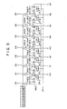
- Fig. 6 shows a divider for dividing the element of the Galois field GF(2 m ) in such a manner as described above.
- dividend ⁇ i and divider ⁇ j are multiplied by a 64, ⁇ 128 or a 192 before they are supplied to the linear shift registers.
- divider data ⁇ j are supplied to a linear shift register A 1 , to a linear shift register A 2 through an a 64 multiplier circuit 51, to a linear shift register A3 through an a 128 multiplier circuit 52 and to a linear shift register A4 through an ⁇ 192 multiplier circuit 53.
- These linear shift registers A 1 , A 2 , A3 and A4 are identical to the linear shift register SR 0 shown in Fig. 5. They are shifted by a clock pulse Cp supplied through an AND gate AND 11 . Every time they are shifted, the data stored in them are multiplied by a.
- the outputs of the linear shift registers A 1 , A 2 , A3 and A4 are supplied to "1" detector circuits 54, 55, 56 and 57, respectively.
- the outputs of the "1" detector circuits 54, 55, 56 and 57 are coupled to a 4-input NOR gate NOR 10 .
- the output of the NOR gate NOR 10 is coupled to one input of the AND gate AND 11 , the other input of which is connected to receive a clock pulse Cp.
- Dividend data ⁇ i are supplied to a linear shift register B 1 , a linear shift register B 2 through an a 64 multiplier circuit 58, a linear shift register B 3 through an a 128 multiplier circuit 59 and a linear shift register B 4 through an a 192 multiplier circuit 60. They are shifted by a clock pulse Cp supplied through the AND gate AND 11 . Every time they are shifted, the data stored in them are multiplied by a.
- the outputs of the linear shift registers B l , B 2 , B 3 and B 4 are supplied to AND circuits 61, 62, 63 and 64, respectively.
- the AND circuits 61, 62, 63 and 64 are connected to the outputs of the "1" detector circuits 54, 55, 56 and 57, respectively.
- the AND circuit 61 supplies the logical product of the outputs from the "1" detector circuit 54 and shift register B l .
- the AND circuit 62 produces the logical product of the outputs from the "1" detector circuit 55 and shift register B 2 .
- the AND circuits 63 and 64 generate the logical product of the outputs from the "1" detector circuit 56 and shift register B 3 and the logical product of the outputs from the "1" detector circuit 57 and shift register B 4 , respectively.
- the outputs from the AND circuits 61 to 64 are supplied to a 4-input OR circuit 65, whereby element a i is divided by element ⁇ j .
- each linear shift register is an 8-bit register.
- the "1" detector circuits 54 to 57 have the same structure.
- each "1" detector circuit is a NOR gate NOR 11 having eight input terminals. Only the bit of the shift register which corresponds to a l is coupled to the first input terminal of the NOR gate NOR 11 through an inverter I 10 . The second to eighth bits of the register are directly connected to the second to eighth input terminals of the NOR gate NOR 11 , respectively.
- each AND circuit consists of eight AND gates AND 20 to AND 27 each with two input terminals.
- the AND gates AND 20 to AND 27 are connected at one input terminal to the corresponding linear shift register B l , B 2 , B 3 or B 4 which are 8-bit registers. More precisely, the AND gates AND 20 to AND 27 are connected at one input terminal to the first to eighth bits of the linear shift register, respectively.
- the AND gates AND 20 to AND 27 are coupled at the other input terminal to the corresponding "1" detector circuit 54, 55, 56 or 57.
- Fig. 9 shows the OR circuit 65 used in the divider shown in Fig. 6.
- the OR circuit 65 consists of eight 4-input OR gates OR 20 to OR 27 .
- the OR gates OR 20 to OR 27 are connected at the first input terminal to the outputs of the eight AND gates of the AND circuit 61, respectively. They are coupled at the second input terminal to the outputs of the eight AND gates of the AND circuit 62. They are coupled at the third input terminal to the outputs of the eight AND gates of the AND circuit 63. And they are connected to the 4-input terminal to the outputs of the eight AND gates of the AND circuit 64, respectively.
- Fig. 10 shows the a 64 multiplier circuit 58 used in the divider shown in Fig. 6.
- the circuit 58 is designed upon the assumption that divider ⁇ j is given as follows: where b 1 to b 7 are 0 or 1. Since
- the a 128 multiplier circuit 59 and the ⁇ 192 multiplier circuit 60 have structures which are similar to that of the a 64 multiplier circuit 58.
- the divider shown in Fig. 6 divides ⁇ 200 by a 1 8 0 in the following manner, thus providing data representing a 20.
- divider data a 180 are stored in the linear shift registers A l to A4 and dividend data a 200 are stored in the linear shift registers B l to B 4 , as shown below:
- clock pulses Cp are supplied from the AND gate AND 11 to the linear shift registers A 1 to A4 and the linear shift registers B l to B 4 .
- the "1" detector circuit 55 detects this, and the NOR gate NOR 10 supplies an output of logical "0" to the AND gate AND 11 .
- the AND gate AND 11 stops supplying clock pulses Cp to the registers A 1 to A4 and B 1 to B 4 .
- the data stored in the register B 2 represent a 20 .
- the data representing a 20 i.e., the quotient of the division a 200 ⁇ a 1 80, are supplied through the AND circuit 62 and the OR circuit 65.
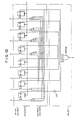
- Fig. 11 shows another divider according to the present invention, which can divide the elements of the Galois field GF(2 8 ) by performing multiplications of the elements.
- dividend ⁇ i and divider ⁇ j are multiplied by ⁇ 1 , ⁇ 2 and a3 before they are supplied to the linear shift registers.
- Both dividend ⁇ i and divider ⁇ j are then multiplied by a4 in the linear shift registers.
- divider data ⁇ j are supplied to a linear shift register A 1 , to a linear shift register A 2 through an a l multiplier circuit 51, to a linear shift register A3 through an a 2 multiplier circuit 52, and to a linear shift register A4 through an a3 multiplier circuit 53.
- the linear shift registers A 1 , A 2 , A3 and A4 are identical and have a structure as shown in Fig. 12.
- Each of the linear shift registers A 1 to A4 is an 8-bit register. It comprises flip-flop circuits FF 10 to FF 17 and exclusive-OR gates EX-OR 10 to EX-OR 31 .
- the flip-flop circuits FF 10 to FF 17 are cascade-connected and feedback-connected by the exclusive-OR gates EX-OR 10 to EX-OR 31 . Every time a clock pulse Cp is supplied to the linear shift registers A l to A4 from an AND gate AND 10 shown in Fig. 11, the registers A l to A4 are shifted to multiply the data stored in them by a4.
- the outputs of the linear shift registers Al, A2, A3 and A4 are connected to "1" detector circuits 54, 55, 56 and 57, respectively.
- Each of the "1" detector circuits 54 to 57 consists of one inverter I 10 and an 8-input NOR gate NOR 10 as shown in Fig. 12. It generates an output signal of logical "1" when the contents of the linear shift register connected to it are "10000000".
- the outputs of the "1" detector circuit 54, 55, 56 and 57 are coupled to the input terminals of a 4-input NOR gate NOR 11 (Fig. 11), respectively.
- the NOR gate NOR 11 generates an output signal of logical "0" when any one of the "1" detector circuits 54 to 57 generates an output of logical "1".
- the output of the NOR gate NOR 11 is connected to the AND gate AND 10 . Hence, when an output of logical "0" is supplied from the NOR gate NOR 11 to the AND gate AND 10 , the AND gate AND 10 stops supplying clock pulses Cp.
- Dividend data a i are supplied to a linear shift register B 1 , to a linear shift register B 2 through an a l multiplier circuit 58, to a linear shift register B 3 through an a 2 multiplier circuit 59 and to a linear shift register B 4 through an a3 multiplier circuit 60.
- the linear shift registers B l to B 4 are shifted every time they receive a clock pulse Cp from the AND gate AND 10 , thereby multiplying the data stored in them by a4.
- the outputs of the linear shift registers B l , B 2 , B 3 and B 4 are connected to AND circuits 61, 62, 63 and 64, respectively.
- the outputs of the "1" detector circuits 54, 55, 56 and 57 are connected to the AND circuits 61, 62, 63 and 64, respectively.
- the AND circuit 61 generates the logical product of the outputs from the "1" detector circuit 54 and shift register B 1 .
- the AND circuit 62 produces the logical product of the outputs from the "1" detector circuit 55 and shift register B 2 .
- the AND circuit 63 supplies the logical product of the outputs from the "1" detector circuit 56 and shift register B 3 .
- the AND circuit 64 generates the logical product of the outputs from the "1" detector circuit 57 and shift register B 4 .
- the outputs from the AND circuits 61 to 64 are supplied to a 4-input OR circuit 65, whereby element a i is divided by element aj.
- each of the AND circuits 61 to 64 consists of eight AND gates AND 20 to AND 27 each with two input terminals.
- the AND gates AND 20 to AND 27 are connected at one input terminal to the corresponding linear shift registers B l , B 2 , B 3 and B 4 which are 8-bit registers. More precisely, the AND gates AND 20 to AND 27 are coupled at one input terminal to the first to eighth bits of the linear shift register, respectively.
- the AND gates AND 20 to AND 27 are coupled at the other input terminal to the corresponding "1" detector circuit 54, 55, 56 or 57.
- the OR circuit 65 is identical with the circuit shown in Fig. 9. It consists of eight 4-input OR gates OR 20 to OR 27 .
- the OR gates OR 20 to OR 27 are connected at the first input terminal to the outputs of the eight AND gates of the AND circuit 61, respectively. They are coupled at the second input terminal to the outputs of the eight AND gates of the AND circuit 62. They are coupled at the third input terminal to the outputs of the eight AND gates of the AND circuit 63. And they are connected at the fourth input terminal to the outputs of the eight AND gates of the AND circuit 64, respectively.
- Fig. 13 shows the a l multiplier circuit 58 used in the divider shown in Fig. 11.
- the a l multiplier circuit 58 is designed upon the assumption that divider ⁇ j is given as follows:
- ⁇ ⁇ B(a) is expressed as follows:
- the ⁇ l multiplier circuit 58 is comprised of exclusive-OR gates EX-OR 32 to EX-OR 34 which are connected as shown in Fig. 13.
- the circuit 58 receives input data representing B(a), it generates output data representing ⁇ ⁇ B(a), i.e. the product of B(a) and a.
- the a 2 multiplier circuit 59 and the a3 mutliplier circuit 60 have structures which are similar to that of the a l multiplier circuit 68.
- the divider shown in Fig. 11 divides element ⁇ i of the Galois field GF(2 8 ) by element ⁇ j of the Galois field GF (2 8 ) in the following manner.
- divider data aj are supplied to the linear shift register A 1 , to the linear shift register A 2 through the a l multiplier circuit 51, to the linear shift register A3 through the a 2 multiplier 52 and to the linear shift register A4 through the a3 multiplier circuit 53.
- dividend data a l are supplied to the linear shift register B 1 , to the linear shift register B 2 through the a l multiplier circuit 58, to the linear shift register B 3 through the a 2 multiplier circuit 59 and to the linear shift register B 4 through the a3 multiplier circuit 60.
- the data stored in the shift registers A 1 to A4 and the shift registers B 1 to B 4 are as listed below:
- clock pulses Cp are supplied from the AND gate AND 10 to the linear shift registers A 1 to A4 and the linear shift registers B l to B 4 .
- the shift registers A 1 to A4 and B l to B 4 receive a clock pulse C p , they are shifted, thereby multiplying the data stored in them by a4.
- the "1" detector circuit connected to the shift register generates an output signal of logical "1".
- the AND gate AND 10 stops supplying clock pulses Cp to the shift registers A 1 to A4 and B 1 to B 4 .
- the contents of the linear shift register B 1 , B 2 , B 3 or B 4 which represent the quotient of division ⁇ i ⁇ ⁇ j , are delivered from the OR circuit 65.
- divider data a 240 are supplied to the linear shift register A 1 .
- the data are supplied also to the linear shift registers A 2 , A 3 and A4 through the a l multiplier circuit 51, a 2 multiplier circuit 52 and a3 multiplier circuit 53, respectively.
- dividend data ⁇ 10 are supplied to the linear shift register B l .
- the data ⁇ 10 are also supplied to the linear shift register B 2 , B 3 and B 4 through the a l multiplier circuit 58, a 2 multiplier circuit 59 and a3 multiplier circuit 60, respectively.
- the shift registers A 1 to A4 and the shift registers B 1 to B 4 then store the data listed below:
- Clock pulses Cp are then supplied one after another from the AND gate 10 to the shift registers A 1 to A4 and B 1 to B 4 .
- the shift registers A 1 to A4 and B 1 to B 4 store the following data:
- the data a 25 stored in the shift register B 4 which corresponds to the register A4 are therefore supplied as the quotient from the OR circuit 65.
- the linear shift registers A 1 to A4 and B l to B 4 multiply the data stored in them by a4 every time they are shifted.
- Two linear shift registers A 5 and B 5 may be used in addition to the shift registers A 1 to A4 and B 1 to B 4 and two a 5 multiplier circuits may be connected to the inputs of the registers A 5 and B 5 , respectively.
- the division a i - ⁇ j can be performed by multiplying both dividend a i and divider ⁇ j by a, 50 times at least.
- the apparatus of the invention may be used in combination with a system for recording, reproducing and transmitting digital data such as PCM data, a system for processing such data or any other system in which one of the elements of the Galois field needs to be divided by another element of the Galois field.
- the present invention can provide an apparatus for dividing the elements of a Galois field, which has neither a logarithm buffer nor an antilogarithm buffer, both of which need to have a large memory capacity, and which therefore has a simple structure and can be manufactured inexpensively, and which can still operate at a high speed.
Landscapes
- Engineering & Computer Science (AREA)
- Physics & Mathematics (AREA)
- General Physics & Mathematics (AREA)
- Theoretical Computer Science (AREA)
- Pure & Applied Mathematics (AREA)
- Computational Mathematics (AREA)
- Mathematical Analysis (AREA)
- Mathematical Optimization (AREA)
- Mathematical Physics (AREA)
- General Engineering & Computer Science (AREA)
- Computing Systems (AREA)
- Algebra (AREA)
- Probability & Statistics with Applications (AREA)
- Multimedia (AREA)
- Signal Processing (AREA)
- Quality & Reliability (AREA)
- Error Detection And Correction (AREA)
Applications Claiming Priority (4)
| Application Number | Priority Date | Filing Date | Title |
|---|---|---|---|
| JP102805/82 | 1982-06-15 | ||
| JP102803/82 | 1982-06-15 | ||
| JP57102803A JPS58219647A (ja) | 1982-06-15 | 1982-06-15 | ガロア体における除算装置 |
| JP57102805A JPS58219649A (ja) | 1982-06-15 | 1982-06-15 | ガロア体における除算装置 |
Publications (3)
| Publication Number | Publication Date |
|---|---|
| EP0096163A2 true EP0096163A2 (fr) | 1983-12-21 |
| EP0096163A3 EP0096163A3 (en) | 1984-10-17 |
| EP0096163B1 EP0096163B1 (fr) | 1988-06-01 |
Family
ID=26443482
Family Applications (1)
| Application Number | Title | Priority Date | Filing Date |
|---|---|---|---|
| EP83102173A Expired EP0096163B1 (fr) | 1982-06-15 | 1983-03-05 | Appareil pour diviser les éléments d'un champ de Galois |
Country Status (4)
| Country | Link |
|---|---|
| US (1) | US4574361A (fr) |
| EP (1) | EP0096163B1 (fr) |
| KR (1) | KR860000902B1 (fr) |
| DE (1) | DE3376907D1 (fr) |
Cited By (6)
| Publication number | Priority date | Publication date | Assignee | Title |
|---|---|---|---|---|
| EP0152702A3 (en) * | 1983-12-30 | 1986-10-01 | Sony Corporation | Arithmetic circuit of finite field |
| EP0158510A3 (en) * | 1984-04-06 | 1988-08-31 | Ampex Corporation | Error detection and correction in digital communication systems |
| US5068857A (en) * | 1988-09-02 | 1991-11-26 | Mitsubishi Denki Kabushiki Kaisha | Error correction circuit |
| GB2253975A (en) * | 1991-03-20 | 1992-09-23 | Samsung Electronics Co Ltd | Processing images, sound or data encoded in error correcting code using Galois Field arithmetic |
| EP0262944B1 (fr) * | 1986-09-30 | 1994-03-09 | Canon Kabushiki Kaisha | Appareil de correction d'erreurs |
| FR2698703A1 (fr) * | 1992-11-30 | 1994-06-03 | Samsung Electronics Co Ltd | Procédé et dispositif de production de l'inverse d'un élément arbitraire dans un champ fini. |
Families Citing this family (21)
| Publication number | Priority date | Publication date | Assignee | Title |
|---|---|---|---|---|
| WO1985003371A1 (fr) * | 1984-01-21 | 1985-08-01 | Sony Corporation | Circuit de calcul de champs finis |
| US4723243A (en) * | 1985-12-02 | 1988-02-02 | Advanced Micro Devices, Inc. | CRC calculation machine with variable bit boundary |
| US4720831A (en) * | 1985-12-02 | 1988-01-19 | Advanced Micro Devices, Inc. | CRC calculation machine with concurrent preset and CRC calculation function |
| US4891781A (en) * | 1987-03-04 | 1990-01-02 | Cylink Corporation | Modulo arithmetic processor chip |
| AU613701B2 (en) * | 1987-06-26 | 1991-08-08 | Digital Equipment Corporation | Apparatus for computing multiplicative inverses in data encoding decoding devices |
| US4975867A (en) * | 1987-06-26 | 1990-12-04 | Digital Equipment Corporation | Apparatus for dividing elements of a Galois Field GF (2QM) |
| EP0431629A3 (en) * | 1989-12-08 | 1993-07-21 | Sony Corporation | Mutual division circuit |
| US4994995A (en) * | 1990-03-14 | 1991-02-19 | International Business Machines Corporation | Bit-serial division method and apparatus |
| US5210710A (en) * | 1990-10-17 | 1993-05-11 | Cylink Corporation | Modulo arithmetic processor chip |
| JP3232602B2 (ja) * | 1991-09-06 | 2001-11-26 | ソニー株式会社 | ユークリッドの互除回路 |
| US5442578A (en) * | 1991-12-12 | 1995-08-15 | Sony Corporation | Calculating circuit for error correction |
| ES2099789T3 (es) * | 1992-07-14 | 1997-06-01 | Alcatel Bell Nv | Dispositivo divisor para dividir un primer polinomio por un segundo polinomio. |
| US5379243A (en) * | 1992-08-31 | 1995-01-03 | Comstream Corporation | Method and apparatus for performing finite field division |
| JP2694792B2 (ja) * | 1993-01-27 | 1997-12-24 | 日本電気株式会社 | 誤り位置多項式演算回路 |
| US5493522A (en) * | 1994-09-21 | 1996-02-20 | Northrop Grumman Corporation | Fast arithmetic modulo divider |
| US5939693A (en) * | 1998-02-02 | 1999-08-17 | Motorola Inc. | Polynomial calculator device, and method therefor |
| US6923726B1 (en) | 1999-08-25 | 2005-08-02 | Voith Turbo Gmbh & Co., Kg | Articulated yoke, method for the production of a supporting surface enabling an even distribution and bearing arrangement |
| KR100478974B1 (ko) * | 2002-12-03 | 2005-03-25 | 한국전자통신연구원 | 직렬 유한체 승산기 |
| JP4891704B2 (ja) * | 2006-08-28 | 2012-03-07 | 株式会社東芝 | 半導体記憶装置 |
| JP5267038B2 (ja) * | 2008-10-20 | 2013-08-21 | 富士通株式会社 | 線形帰還シフト演算装置、通信装置、マイクロプロセッサ、及び線形帰還シフト演算装置におけるデータ出力方法 |
| JP5259343B2 (ja) * | 2008-10-31 | 2013-08-07 | 株式会社東芝 | メモリ装置 |
Family Cites Families (6)
| Publication number | Priority date | Publication date | Assignee | Title |
|---|---|---|---|---|
| US3828175A (en) * | 1972-10-30 | 1974-08-06 | Amdahl Corp | Method and apparatus for division employing table-lookup and functional iteration |
| US4099160A (en) * | 1976-07-15 | 1978-07-04 | International Business Machines Corporation | Error location apparatus and methods |
| US4142174A (en) * | 1977-08-15 | 1979-02-27 | International Business Machines Corporation | High speed decoding of Reed-Solomon codes |
| DE2855807A1 (de) * | 1978-12-22 | 1980-06-26 | Siemens Ag | Schaltungsanordnung zur korrektur von bytestrukturierten fehlern |
| CA1170776A (fr) * | 1980-07-18 | 1984-07-10 | Yoichiro Sako | Methode de correction d'erreurs dans des blocs de donnees |
| JPS57155667A (en) * | 1981-03-23 | 1982-09-25 | Sony Corp | Arithmetic circuit of galois matter |
-
1983
- 1983-03-05 EP EP83102173A patent/EP0096163B1/fr not_active Expired
- 1983-03-05 DE DE8383102173T patent/DE3376907D1/de not_active Expired
- 1983-03-10 US US06/473,765 patent/US4574361A/en not_active Expired - Lifetime
- 1983-06-15 KR KR8302663A patent/KR860000902B1/ko not_active Expired
Non-Patent Citations (1)
| Title |
|---|
| "PETERSON: Error-correction codes", 1972, MIT PRESS, pages: 178 - 180 |
Cited By (10)
| Publication number | Priority date | Publication date | Assignee | Title |
|---|---|---|---|---|
| EP0152702A3 (en) * | 1983-12-30 | 1986-10-01 | Sony Corporation | Arithmetic circuit of finite field |
| EP0158510A3 (en) * | 1984-04-06 | 1988-08-31 | Ampex Corporation | Error detection and correction in digital communication systems |
| EP0262944B1 (fr) * | 1986-09-30 | 1994-03-09 | Canon Kabushiki Kaisha | Appareil de correction d'erreurs |
| EP0566215A3 (en) * | 1986-09-30 | 1994-05-18 | Canon Kk | Error correction apparatus |
| US5590138A (en) * | 1986-09-30 | 1996-12-31 | Canon Kabushiki Kaisha | Error correction apparatus |
| US5774389A (en) * | 1986-09-30 | 1998-06-30 | Canon Kabushiki Kaisha | Error correction apparatus |
| US5068857A (en) * | 1988-09-02 | 1991-11-26 | Mitsubishi Denki Kabushiki Kaisha | Error correction circuit |
| GB2253975A (en) * | 1991-03-20 | 1992-09-23 | Samsung Electronics Co Ltd | Processing images, sound or data encoded in error correcting code using Galois Field arithmetic |
| GB2253975B (en) * | 1991-03-20 | 1994-05-25 | Samsung Electronics Co Ltd | An apparatus operating on a galois field over gf (2m) |
| FR2698703A1 (fr) * | 1992-11-30 | 1994-06-03 | Samsung Electronics Co Ltd | Procédé et dispositif de production de l'inverse d'un élément arbitraire dans un champ fini. |
Also Published As
| Publication number | Publication date |
|---|---|
| KR860000902B1 (en) | 1986-07-16 |
| KR840005228A (ko) | 1984-11-05 |
| US4574361A (en) | 1986-03-04 |
| EP0096163B1 (fr) | 1988-06-01 |
| DE3376907D1 (en) | 1988-07-07 |
| EP0096163A3 (en) | 1984-10-17 |
Similar Documents
| Publication | Publication Date | Title |
|---|---|---|
| EP0096163B1 (fr) | Appareil pour diviser les éléments d'un champ de Galois | |
| EP0096165B1 (fr) | Appareil pour diviser les éléments d'un champ de Galois | |
| EP0096109B1 (fr) | Système de correction d'erreurs | |
| EP0329789B1 (fr) | Unite arithmetique a champ de galois | |
| EP0136587B1 (fr) | Circuit de correction d'erreur | |
| EP0787325A1 (fr) | Procede et appareil de correction d'erreurs pour emulateur d'unite de disques | |
| JPH0553087B2 (fr) | ||
| JPH0653842A (ja) | Rsコードデータ信号を復号化する方法および回路 | |
| EP0781471B1 (fr) | Systeme verificateur a code detecteur d'erreur/controle de redondance cyclique | |
| US5541940A (en) | Error correction method and error correction circuit | |
| JPS638648B2 (fr) | ||
| JPS6237415B2 (fr) | ||
| JPH09305572A (ja) | ガロア体の除算方法および除算装置 | |
| JPS638650B2 (fr) | ||
| EP1037148B1 (fr) | Méthode de codage d'erreurs | |
| JPS638649B2 (fr) | ||
| JPS6248254B2 (fr) | ||
| JPS6237414B2 (fr) | ||
| JPS6246018B2 (fr) | ||
| JPH0834439B2 (ja) | ガロア体演算装置 | |
| JPS63131623A (ja) | チエンのアルゴリズム実現装置 | |
| JP2553571B2 (ja) | ガロア体演算装置 | |
| JPH10150367A (ja) | 誤り訂正装置 | |
| JP2002207593A (ja) | ガロア体乗算器およびガロア体除算器 | |
| KR19980031192A (ko) | 확장된 신드롬 다항식 생성 장치 |
Legal Events
| Date | Code | Title | Description |
|---|---|---|---|
| PUAI | Public reference made under article 153(3) epc to a published international application that has entered the european phase |
Free format text: ORIGINAL CODE: 0009012 |
|
| 17P | Request for examination filed |
Effective date: 19830305 |
|
| AK | Designated contracting states |
Designated state(s): DE FR GB NL |
|
| PUAL | Search report despatched |
Free format text: ORIGINAL CODE: 0009013 |
|
| RAP1 | Party data changed (applicant data changed or rights of an application transferred) |
Owner name: KABUSHIKI KAISHA TOSHIBA |
|
| AK | Designated contracting states |
Designated state(s): DE FR GB NL |
|
| 17Q | First examination report despatched |
Effective date: 19860516 |
|
| GRAA | (expected) grant |
Free format text: ORIGINAL CODE: 0009210 |
|
| AK | Designated contracting states |
Kind code of ref document: B1 Designated state(s): DE FR GB NL |
|
| REF | Corresponds to: |
Ref document number: 3376907 Country of ref document: DE Date of ref document: 19880707 |
|
| ET | Fr: translation filed | ||
| PLBE | No opposition filed within time limit |
Free format text: ORIGINAL CODE: 0009261 |
|
| STAA | Information on the status of an ep patent application or granted ep patent |
Free format text: STATUS: NO OPPOSITION FILED WITHIN TIME LIMIT |
|
| 26N | No opposition filed | ||
| REG | Reference to a national code |
Ref country code: GB Ref legal event code: 746 Effective date: 19981126 |
|
| PGFP | Annual fee paid to national office [announced via postgrant information from national office to epo] |
Ref country code: NL Payment date: 20000330 Year of fee payment: 18 |
|
| REG | Reference to a national code |
Ref country code: FR Ref legal event code: D6 |
|
| PG25 | Lapsed in a contracting state [announced via postgrant information from national office to epo] |
Ref country code: NL Free format text: LAPSE BECAUSE OF NON-PAYMENT OF DUE FEES Effective date: 20011001 |
|
| NLV4 | Nl: lapsed or anulled due to non-payment of the annual fee |
Effective date: 20011001 |
|
| REG | Reference to a national code |
Ref country code: GB Ref legal event code: IF02 |
|
| PGFP | Annual fee paid to national office [announced via postgrant information from national office to epo] |
Ref country code: GB Payment date: 20020306 Year of fee payment: 20 |
|
| PGFP | Annual fee paid to national office [announced via postgrant information from national office to epo] |
Ref country code: FR Payment date: 20020312 Year of fee payment: 20 |
|
| PGFP | Annual fee paid to national office [announced via postgrant information from national office to epo] |
Ref country code: DE Payment date: 20020320 Year of fee payment: 20 |
|
| PG25 | Lapsed in a contracting state [announced via postgrant information from national office to epo] |
Ref country code: GB Free format text: LAPSE BECAUSE OF EXPIRATION OF PROTECTION Effective date: 20030304 |
|
| REG | Reference to a national code |
Ref country code: GB Ref legal event code: PE20 Effective date: 20030304 |