EP0096501B1 - Verfahren zur Wahrnehmung eines Feuers - Google Patents
Verfahren zur Wahrnehmung eines Feuers Download PDFInfo
- Publication number
- EP0096501B1 EP0096501B1 EP83302969A EP83302969A EP0096501B1 EP 0096501 B1 EP0096501 B1 EP 0096501B1 EP 83302969 A EP83302969 A EP 83302969A EP 83302969 A EP83302969 A EP 83302969A EP 0096501 B1 EP0096501 B1 EP 0096501B1
- Authority
- EP
- European Patent Office
- Prior art keywords
- layer
- gold
- absorber layer
- absorber
- film
- Prior art date
- Legal status (The legal status is an assumption and is not a legal conclusion. Google has not performed a legal analysis and makes no representation as to the accuracy of the status listed.)
- Expired
Links
- 238000000034 method Methods 0.000 title claims description 45
- 239000006096 absorbing agent Substances 0.000 claims description 120
- 239000010931 gold Substances 0.000 claims description 78
- 229910052737 gold Inorganic materials 0.000 claims description 60
- PCHJSUWPFVWCPO-UHFFFAOYSA-N gold Chemical compound [Au] PCHJSUWPFVWCPO-UHFFFAOYSA-N 0.000 claims description 57
- 239000000758 substrate Substances 0.000 claims description 25
- ATJFFYVFTNAWJD-UHFFFAOYSA-N Tin Chemical compound [Sn] ATJFFYVFTNAWJD-UHFFFAOYSA-N 0.000 claims description 17
- 229920000642 polymer Polymers 0.000 claims description 17
- 229910001020 Au alloy Inorganic materials 0.000 claims description 13
- 239000003353 gold alloy Substances 0.000 claims description 10
- 238000005054 agglomeration Methods 0.000 claims description 8
- 230000002776 aggregation Effects 0.000 claims description 8
- 229910052787 antimony Inorganic materials 0.000 claims description 7
- WATWJIUSRGPENY-UHFFFAOYSA-N antimony atom Chemical compound [Sb] WATWJIUSRGPENY-UHFFFAOYSA-N 0.000 claims description 7
- 238000001514 detection method Methods 0.000 claims description 6
- 238000005275 alloying Methods 0.000 claims 1
- 239000010410 layer Substances 0.000 description 141
- 239000010408 film Substances 0.000 description 94
- 230000003287 optical effect Effects 0.000 description 48
- 125000006850 spacer group Chemical group 0.000 description 31
- VYPSYNLAJGMNEJ-UHFFFAOYSA-N Silicium dioxide Chemical compound O=[Si]=O VYPSYNLAJGMNEJ-UHFFFAOYSA-N 0.000 description 23
- 239000000463 material Substances 0.000 description 22
- 229910052714 tellurium Inorganic materials 0.000 description 22
- PORWMNRCUJJQNO-UHFFFAOYSA-N tellurium atom Chemical compound [Te] PORWMNRCUJJQNO-UHFFFAOYSA-N 0.000 description 22
- 230000035945 sensitivity Effects 0.000 description 21
- 238000000151 deposition Methods 0.000 description 17
- 238000002310 reflectometry Methods 0.000 description 13
- 239000011800 void material Substances 0.000 description 13
- 230000005855 radiation Effects 0.000 description 12
- 230000008021 deposition Effects 0.000 description 10
- 230000008018 melting Effects 0.000 description 10
- 238000002844 melting Methods 0.000 description 10
- 229910052751 metal Inorganic materials 0.000 description 9
- 239000002184 metal Substances 0.000 description 9
- 238000003860 storage Methods 0.000 description 9
- 229910052782 aluminium Inorganic materials 0.000 description 7
- XAGFODPZIPBFFR-UHFFFAOYSA-N aluminium Chemical compound [Al] XAGFODPZIPBFFR-UHFFFAOYSA-N 0.000 description 7
- 229910045601 alloy Inorganic materials 0.000 description 6
- 239000000956 alloy Substances 0.000 description 6
- 238000012544 monitoring process Methods 0.000 description 6
- 239000000377 silicon dioxide Substances 0.000 description 6
- 238000001228 spectrum Methods 0.000 description 6
- 239000011248 coating agent Substances 0.000 description 5
- 238000000576 coating method Methods 0.000 description 5
- 230000000694 effects Effects 0.000 description 5
- 230000003667 anti-reflective effect Effects 0.000 description 4
- 230000008901 benefit Effects 0.000 description 4
- 230000015572 biosynthetic process Effects 0.000 description 4
- 239000011521 glass Substances 0.000 description 4
- 230000006872 improvement Effects 0.000 description 4
- 238000001000 micrograph Methods 0.000 description 4
- 230000006911 nucleation Effects 0.000 description 4
- 238000010899 nucleation Methods 0.000 description 4
- 239000011669 selenium Substances 0.000 description 4
- 230000008859 change Effects 0.000 description 3
- 238000013500 data storage Methods 0.000 description 3
- 230000001747 exhibiting effect Effects 0.000 description 3
- 230000003647 oxidation Effects 0.000 description 3
- 238000007254 oxidation reaction Methods 0.000 description 3
- 238000002360 preparation method Methods 0.000 description 3
- 230000008569 process Effects 0.000 description 3
- 238000012552 review Methods 0.000 description 3
- 229910052711 selenium Inorganic materials 0.000 description 3
- 238000012360 testing method Methods 0.000 description 3
- 239000010409 thin film Substances 0.000 description 3
- VYZAMTAEIAYCRO-UHFFFAOYSA-N Chromium Chemical compound [Cr] VYZAMTAEIAYCRO-UHFFFAOYSA-N 0.000 description 2
- PXHVJJICTQNCMI-UHFFFAOYSA-N Nickel Chemical compound [Ni] PXHVJJICTQNCMI-UHFFFAOYSA-N 0.000 description 2
- KDLHZDBZIXYQEI-UHFFFAOYSA-N Palladium Chemical compound [Pd] KDLHZDBZIXYQEI-UHFFFAOYSA-N 0.000 description 2
- 241000243142 Porifera Species 0.000 description 2
- BUGBHKTXTAQXES-UHFFFAOYSA-N Selenium Chemical compound [Se] BUGBHKTXTAQXES-UHFFFAOYSA-N 0.000 description 2
- 239000004809 Teflon Substances 0.000 description 2
- 229920006362 Teflon® Polymers 0.000 description 2
- 239000004411 aluminium Substances 0.000 description 2
- 230000005540 biological transmission Effects 0.000 description 2
- 229910052797 bismuth Inorganic materials 0.000 description 2
- JCXGWMGPZLAOME-UHFFFAOYSA-N bismuth atom Chemical compound [Bi] JCXGWMGPZLAOME-UHFFFAOYSA-N 0.000 description 2
- 229910052804 chromium Inorganic materials 0.000 description 2
- 239000011651 chromium Substances 0.000 description 2
- 238000010549 co-Evaporation Methods 0.000 description 2
- 238000013461 design Methods 0.000 description 2
- 238000001704 evaporation Methods 0.000 description 2
- 230000006870 function Effects 0.000 description 2
- 239000005350 fused silica glass Substances 0.000 description 2
- 238000010438 heat treatment Methods 0.000 description 2
- 238000002955 isolation Methods 0.000 description 2
- 238000004519 manufacturing process Methods 0.000 description 2
- BASFCYQUMIYNBI-UHFFFAOYSA-N platinum Chemical compound [Pt] BASFCYQUMIYNBI-UHFFFAOYSA-N 0.000 description 2
- 235000012461 sponges Nutrition 0.000 description 2
- 239000011232 storage material Substances 0.000 description 2
- 238000002207 thermal evaporation Methods 0.000 description 2
- 239000010936 titanium Substances 0.000 description 2
- 229910015367 Au—Sb Inorganic materials 0.000 description 1
- GYHNNYVSQQEPJS-UHFFFAOYSA-N Gallium Chemical compound [Ga] GYHNNYVSQQEPJS-UHFFFAOYSA-N 0.000 description 1
- PWHULOQIROXLJO-UHFFFAOYSA-N Manganese Chemical compound [Mn] PWHULOQIROXLJO-UHFFFAOYSA-N 0.000 description 1
- ZOKXTWBITQBERF-UHFFFAOYSA-N Molybdenum Chemical compound [Mo] ZOKXTWBITQBERF-UHFFFAOYSA-N 0.000 description 1
- 229910001245 Sb alloy Inorganic materials 0.000 description 1
- BQCADISMDOOEFD-UHFFFAOYSA-N Silver Chemical compound [Ag] BQCADISMDOOEFD-UHFFFAOYSA-N 0.000 description 1
- 229910001128 Sn alloy Inorganic materials 0.000 description 1
- 229910020935 Sn-Sb Inorganic materials 0.000 description 1
- 229910008757 Sn—Sb Inorganic materials 0.000 description 1
- NINIDFKCEFEMDL-UHFFFAOYSA-N Sulfur Chemical compound [S] NINIDFKCEFEMDL-UHFFFAOYSA-N 0.000 description 1
- 239000005864 Sulphur Substances 0.000 description 1
- 229910001215 Te alloy Inorganic materials 0.000 description 1
- RTAQQCXQSZGOHL-UHFFFAOYSA-N Titanium Chemical compound [Ti] RTAQQCXQSZGOHL-UHFFFAOYSA-N 0.000 description 1
- HCHKCACWOHOZIP-UHFFFAOYSA-N Zinc Chemical compound [Zn] HCHKCACWOHOZIP-UHFFFAOYSA-N 0.000 description 1
- QJVMFBQHKJZFLP-UHFFFAOYSA-N [Au].[Pb].[Au].[Pb].[Au] Chemical compound [Au].[Pb].[Au].[Pb].[Au] QJVMFBQHKJZFLP-UHFFFAOYSA-N 0.000 description 1
- 239000002318 adhesion promoter Substances 0.000 description 1
- 230000032683 aging Effects 0.000 description 1
- 229910021417 amorphous silicon Inorganic materials 0.000 description 1
- 229910052785 arsenic Inorganic materials 0.000 description 1
- RQNWIZPPADIBDY-UHFFFAOYSA-N arsenic atom Chemical compound [As] RQNWIZPPADIBDY-UHFFFAOYSA-N 0.000 description 1
- 229910000416 bismuth oxide Inorganic materials 0.000 description 1
- 229910052793 cadmium Inorganic materials 0.000 description 1
- BDOSMKKIYDKNTQ-UHFFFAOYSA-N cadmium atom Chemical compound [Cd] BDOSMKKIYDKNTQ-UHFFFAOYSA-N 0.000 description 1
- 238000004140 cleaning Methods 0.000 description 1
- 229910017052 cobalt Inorganic materials 0.000 description 1
- 239000010941 cobalt Substances 0.000 description 1
- GUTLYIVDDKVIGB-UHFFFAOYSA-N cobalt atom Chemical compound [Co] GUTLYIVDDKVIGB-UHFFFAOYSA-N 0.000 description 1
- 230000000052 comparative effect Effects 0.000 description 1
- 230000001010 compromised effect Effects 0.000 description 1
- 239000000470 constituent Substances 0.000 description 1
- 239000000356 contaminant Substances 0.000 description 1
- 229910021419 crystalline silicon Inorganic materials 0.000 description 1
- 230000001351 cycling effect Effects 0.000 description 1
- 230000007547 defect Effects 0.000 description 1
- TYIXMATWDRGMPF-UHFFFAOYSA-N dibismuth;oxygen(2-) Chemical compound [O-2].[O-2].[O-2].[Bi+3].[Bi+3] TYIXMATWDRGMPF-UHFFFAOYSA-N 0.000 description 1
- 239000003989 dielectric material Substances 0.000 description 1
- 238000009792 diffusion process Methods 0.000 description 1
- 239000002355 dual-layer Substances 0.000 description 1
- 239000000428 dust Substances 0.000 description 1
- 238000005566 electron beam evaporation Methods 0.000 description 1
- 238000005516 engineering process Methods 0.000 description 1
- 230000008020 evaporation Effects 0.000 description 1
- 229910052733 gallium Inorganic materials 0.000 description 1
- 229910052732 germanium Inorganic materials 0.000 description 1
- UCHOFYCGAZVYGZ-UHFFFAOYSA-N gold lead Chemical compound [Au].[Pb] UCHOFYCGAZVYGZ-UHFFFAOYSA-N 0.000 description 1
- 238000009499 grossing Methods 0.000 description 1
- 238000005286 illumination Methods 0.000 description 1
- 238000003384 imaging method Methods 0.000 description 1
- 229910052738 indium Inorganic materials 0.000 description 1
- APFVFJFRJDLVQX-UHFFFAOYSA-N indium atom Chemical compound [In] APFVFJFRJDLVQX-UHFFFAOYSA-N 0.000 description 1
- 238000002347 injection Methods 0.000 description 1
- 239000007924 injection Substances 0.000 description 1
- 239000012212 insulator Substances 0.000 description 1
- 238000011835 investigation Methods 0.000 description 1
- 229910052748 manganese Inorganic materials 0.000 description 1
- 239000011572 manganese Substances 0.000 description 1
- 230000007246 mechanism Effects 0.000 description 1
- 230000005012 migration Effects 0.000 description 1
- 238000013508 migration Methods 0.000 description 1
- 239000000203 mixture Substances 0.000 description 1
- 229910052750 molybdenum Inorganic materials 0.000 description 1
- 239000011733 molybdenum Substances 0.000 description 1
- 229910052759 nickel Inorganic materials 0.000 description 1
- 229910000510 noble metal Inorganic materials 0.000 description 1
- 150000002894 organic compounds Chemical class 0.000 description 1
- 229910052763 palladium Inorganic materials 0.000 description 1
- 239000002245 particle Substances 0.000 description 1
- 229910052697 platinum Inorganic materials 0.000 description 1
- 238000007639 printing Methods 0.000 description 1
- 230000001681 protective effect Effects 0.000 description 1
- 238000011084 recovery Methods 0.000 description 1
- 239000003870 refractory metal Substances 0.000 description 1
- 238000009877 rendering Methods 0.000 description 1
- 230000010076 replication Effects 0.000 description 1
- 229910052703 rhodium Inorganic materials 0.000 description 1
- 239000010948 rhodium Substances 0.000 description 1
- MHOVAHRLVXNVSD-UHFFFAOYSA-N rhodium atom Chemical compound [Rh] MHOVAHRLVXNVSD-UHFFFAOYSA-N 0.000 description 1
- 235000012239 silicon dioxide Nutrition 0.000 description 1
- 229910052709 silver Inorganic materials 0.000 description 1
- 239000004332 silver Substances 0.000 description 1
- 239000007787 solid Substances 0.000 description 1
- 238000004544 sputter deposition Methods 0.000 description 1
- 230000035882 stress Effects 0.000 description 1
- 229920001169 thermoplastic Polymers 0.000 description 1
- 239000004416 thermosoftening plastic Substances 0.000 description 1
- 229910052719 titanium Inorganic materials 0.000 description 1
- 238000013519 translation Methods 0.000 description 1
- 238000002834 transmittance Methods 0.000 description 1
- 229910052720 vanadium Inorganic materials 0.000 description 1
- LEONUFNNVUYDNQ-UHFFFAOYSA-N vanadium atom Chemical compound [V] LEONUFNNVUYDNQ-UHFFFAOYSA-N 0.000 description 1
- 238000001429 visible spectrum Methods 0.000 description 1
- XLYOFNOQVPJJNP-UHFFFAOYSA-N water Substances O XLYOFNOQVPJJNP-UHFFFAOYSA-N 0.000 description 1
- 239000001993 wax Substances 0.000 description 1
- 229910052725 zinc Inorganic materials 0.000 description 1
- 239000011701 zinc Substances 0.000 description 1
Images

Classifications
-
- G—PHYSICS
- G11—INFORMATION STORAGE
- G11B—INFORMATION STORAGE BASED ON RELATIVE MOVEMENT BETWEEN RECORD CARRIER AND TRANSDUCER
- G11B7/00—Recording or reproducing by optical means, e.g. recording using a thermal beam of optical radiation by modifying optical properties or the physical structure, reproducing using an optical beam at lower power by sensing optical properties; Record carriers therefor
- G11B7/24—Record carriers characterised by shape, structure or physical properties, or by the selection of the material
- G11B7/2407—Tracks or pits; Shape, structure or physical properties thereof
- G11B7/24085—Pits
-
- G—PHYSICS
- G11—INFORMATION STORAGE
- G11B—INFORMATION STORAGE BASED ON RELATIVE MOVEMENT BETWEEN RECORD CARRIER AND TRANSDUCER
- G11B7/00—Recording or reproducing by optical means, e.g. recording using a thermal beam of optical radiation by modifying optical properties or the physical structure, reproducing using an optical beam at lower power by sensing optical properties; Record carriers therefor
- G11B7/24—Record carriers characterised by shape, structure or physical properties, or by the selection of the material
- G11B7/241—Record carriers characterised by shape, structure or physical properties, or by the selection of the material characterised by the selection of the material
- G11B7/242—Record carriers characterised by shape, structure or physical properties, or by the selection of the material characterised by the selection of the material of recording layers
- G11B7/243—Record carriers characterised by shape, structure or physical properties, or by the selection of the material characterised by the selection of the material of recording layers comprising inorganic materials only, e.g. ablative layers
- G11B2007/24302—Metals or metalloids
- G11B2007/24308—Metals or metalloids transition metal elements of group 11 (Cu, Ag, Au)
-
- G—PHYSICS
- G11—INFORMATION STORAGE
- G11B—INFORMATION STORAGE BASED ON RELATIVE MOVEMENT BETWEEN RECORD CARRIER AND TRANSDUCER
- G11B7/00—Recording or reproducing by optical means, e.g. recording using a thermal beam of optical radiation by modifying optical properties or the physical structure, reproducing using an optical beam at lower power by sensing optical properties; Record carriers therefor
- G11B7/24—Record carriers characterised by shape, structure or physical properties, or by the selection of the material
- G11B7/241—Record carriers characterised by shape, structure or physical properties, or by the selection of the material characterised by the selection of the material
- G11B7/242—Record carriers characterised by shape, structure or physical properties, or by the selection of the material characterised by the selection of the material of recording layers
- G11B7/243—Record carriers characterised by shape, structure or physical properties, or by the selection of the material characterised by the selection of the material of recording layers comprising inorganic materials only, e.g. ablative layers
- G11B2007/24302—Metals or metalloids
- G11B2007/24312—Metals or metalloids group 14 elements (e.g. Si, Ge, Sn)
-
- G—PHYSICS
- G11—INFORMATION STORAGE
- G11B—INFORMATION STORAGE BASED ON RELATIVE MOVEMENT BETWEEN RECORD CARRIER AND TRANSDUCER
- G11B7/00—Recording or reproducing by optical means, e.g. recording using a thermal beam of optical radiation by modifying optical properties or the physical structure, reproducing using an optical beam at lower power by sensing optical properties; Record carriers therefor
- G11B7/24—Record carriers characterised by shape, structure or physical properties, or by the selection of the material
- G11B7/241—Record carriers characterised by shape, structure or physical properties, or by the selection of the material characterised by the selection of the material
- G11B7/242—Record carriers characterised by shape, structure or physical properties, or by the selection of the material characterised by the selection of the material of recording layers
- G11B7/243—Record carriers characterised by shape, structure or physical properties, or by the selection of the material characterised by the selection of the material of recording layers comprising inorganic materials only, e.g. ablative layers
- G11B2007/24302—Metals or metalloids
- G11B2007/24314—Metals or metalloids group 15 elements (e.g. Sb, Bi)
-
- G—PHYSICS
- G11—INFORMATION STORAGE
- G11B—INFORMATION STORAGE BASED ON RELATIVE MOVEMENT BETWEEN RECORD CARRIER AND TRANSDUCER
- G11B7/00—Recording or reproducing by optical means, e.g. recording using a thermal beam of optical radiation by modifying optical properties or the physical structure, reproducing using an optical beam at lower power by sensing optical properties; Record carriers therefor
- G11B7/24—Record carriers characterised by shape, structure or physical properties, or by the selection of the material
- G11B7/241—Record carriers characterised by shape, structure or physical properties, or by the selection of the material characterised by the selection of the material
- G11B7/242—Record carriers characterised by shape, structure or physical properties, or by the selection of the material characterised by the selection of the material of recording layers
- G11B7/243—Record carriers characterised by shape, structure or physical properties, or by the selection of the material characterised by the selection of the material of recording layers comprising inorganic materials only, e.g. ablative layers
- G11B2007/24302—Metals or metalloids
- G11B2007/24316—Metals or metalloids group 16 elements (i.e. chalcogenides, Se, Te)
-
- G—PHYSICS
- G11—INFORMATION STORAGE
- G11B—INFORMATION STORAGE BASED ON RELATIVE MOVEMENT BETWEEN RECORD CARRIER AND TRANSDUCER
- G11B7/00—Recording or reproducing by optical means, e.g. recording using a thermal beam of optical radiation by modifying optical properties or the physical structure, reproducing using an optical beam at lower power by sensing optical properties; Record carriers therefor
- G11B7/24—Record carriers characterised by shape, structure or physical properties, or by the selection of the material
- G11B7/241—Record carriers characterised by shape, structure or physical properties, or by the selection of the material characterised by the selection of the material
- G11B7/252—Record carriers characterised by shape, structure or physical properties, or by the selection of the material characterised by the selection of the material of layers other than recording layers
- G11B7/257—Record carriers characterised by shape, structure or physical properties, or by the selection of the material characterised by the selection of the material of layers other than recording layers of layers having properties involved in recording or reproduction, e.g. optical interference layers or sensitising layers or dielectric layers, which are protecting the recording layers
- G11B2007/25705—Record carriers characterised by shape, structure or physical properties, or by the selection of the material characterised by the selection of the material of layers other than recording layers of layers having properties involved in recording or reproduction, e.g. optical interference layers or sensitising layers or dielectric layers, which are protecting the recording layers consisting essentially of inorganic materials
- G11B2007/2571—Record carriers characterised by shape, structure or physical properties, or by the selection of the material characterised by the selection of the material of layers other than recording layers of layers having properties involved in recording or reproduction, e.g. optical interference layers or sensitising layers or dielectric layers, which are protecting the recording layers consisting essentially of inorganic materials containing group 14 elements except carbon (Si, Ge, Sn, Pb)
-
- G—PHYSICS
- G11—INFORMATION STORAGE
- G11B—INFORMATION STORAGE BASED ON RELATIVE MOVEMENT BETWEEN RECORD CARRIER AND TRANSDUCER
- G11B7/00—Recording or reproducing by optical means, e.g. recording using a thermal beam of optical radiation by modifying optical properties or the physical structure, reproducing using an optical beam at lower power by sensing optical properties; Record carriers therefor
- G11B7/24—Record carriers characterised by shape, structure or physical properties, or by the selection of the material
- G11B7/241—Record carriers characterised by shape, structure or physical properties, or by the selection of the material characterised by the selection of the material
- G11B7/252—Record carriers characterised by shape, structure or physical properties, or by the selection of the material characterised by the selection of the material of layers other than recording layers
- G11B7/257—Record carriers characterised by shape, structure or physical properties, or by the selection of the material characterised by the selection of the material of layers other than recording layers of layers having properties involved in recording or reproduction, e.g. optical interference layers or sensitising layers or dielectric layers, which are protecting the recording layers
- G11B2007/25705—Record carriers characterised by shape, structure or physical properties, or by the selection of the material characterised by the selection of the material of layers other than recording layers of layers having properties involved in recording or reproduction, e.g. optical interference layers or sensitising layers or dielectric layers, which are protecting the recording layers consisting essentially of inorganic materials
- G11B2007/25715—Record carriers characterised by shape, structure or physical properties, or by the selection of the material characterised by the selection of the material of layers other than recording layers of layers having properties involved in recording or reproduction, e.g. optical interference layers or sensitising layers or dielectric layers, which are protecting the recording layers consisting essentially of inorganic materials containing oxygen
-
- G—PHYSICS
- G11—INFORMATION STORAGE
- G11B—INFORMATION STORAGE BASED ON RELATIVE MOVEMENT BETWEEN RECORD CARRIER AND TRANSDUCER
- G11B7/00—Recording or reproducing by optical means, e.g. recording using a thermal beam of optical radiation by modifying optical properties or the physical structure, reproducing using an optical beam at lower power by sensing optical properties; Record carriers therefor
- G11B7/24—Record carriers characterised by shape, structure or physical properties, or by the selection of the material
- G11B7/241—Record carriers characterised by shape, structure or physical properties, or by the selection of the material characterised by the selection of the material
- G11B7/252—Record carriers characterised by shape, structure or physical properties, or by the selection of the material characterised by the selection of the material of layers other than recording layers
- G11B7/254—Record carriers characterised by shape, structure or physical properties, or by the selection of the material characterised by the selection of the material of layers other than recording layers of protective topcoat layers
-
- G—PHYSICS
- G11—INFORMATION STORAGE
- G11B—INFORMATION STORAGE BASED ON RELATIVE MOVEMENT BETWEEN RECORD CARRIER AND TRANSDUCER
- G11B7/00—Recording or reproducing by optical means, e.g. recording using a thermal beam of optical radiation by modifying optical properties or the physical structure, reproducing using an optical beam at lower power by sensing optical properties; Record carriers therefor
- G11B7/24—Record carriers characterised by shape, structure or physical properties, or by the selection of the material
- G11B7/241—Record carriers characterised by shape, structure or physical properties, or by the selection of the material characterised by the selection of the material
- G11B7/252—Record carriers characterised by shape, structure or physical properties, or by the selection of the material characterised by the selection of the material of layers other than recording layers
- G11B7/257—Record carriers characterised by shape, structure or physical properties, or by the selection of the material characterised by the selection of the material of layers other than recording layers of layers having properties involved in recording or reproduction, e.g. optical interference layers or sensitising layers or dielectric layers, which are protecting the recording layers
- G11B7/2572—Record carriers characterised by shape, structure or physical properties, or by the selection of the material characterised by the selection of the material of layers other than recording layers of layers having properties involved in recording or reproduction, e.g. optical interference layers or sensitising layers or dielectric layers, which are protecting the recording layers consisting essentially of organic materials
- G11B7/2575—Record carriers characterised by shape, structure or physical properties, or by the selection of the material characterised by the selection of the material of layers other than recording layers of layers having properties involved in recording or reproduction, e.g. optical interference layers or sensitising layers or dielectric layers, which are protecting the recording layers consisting essentially of organic materials resins
-
- G—PHYSICS
- G11—INFORMATION STORAGE
- G11B—INFORMATION STORAGE BASED ON RELATIVE MOVEMENT BETWEEN RECORD CARRIER AND TRANSDUCER
- G11B7/00—Recording or reproducing by optical means, e.g. recording using a thermal beam of optical radiation by modifying optical properties or the physical structure, reproducing using an optical beam at lower power by sensing optical properties; Record carriers therefor
- G11B7/24—Record carriers characterised by shape, structure or physical properties, or by the selection of the material
- G11B7/241—Record carriers characterised by shape, structure or physical properties, or by the selection of the material characterised by the selection of the material
- G11B7/252—Record carriers characterised by shape, structure or physical properties, or by the selection of the material characterised by the selection of the material of layers other than recording layers
- G11B7/258—Record carriers characterised by shape, structure or physical properties, or by the selection of the material characterised by the selection of the material of layers other than recording layers of reflective layers
- G11B7/2585—Record carriers characterised by shape, structure or physical properties, or by the selection of the material characterised by the selection of the material of layers other than recording layers of reflective layers based on aluminium
Definitions
- the present invention relates to a method for detecting presence of fire or flames.
- Optical storage of digital data is a relatively new technology concerened with the storage and retrieval of digital information utilizing optical techniques, using a special related (ODD, "optical digital data") medium, such as an ODD disk.
- ODD optical digital data
- ODD disk optical digital data
- This disclosure relates to a method for detecting fire or flames using a focused beam of prescribed radiation energy, especially low power laser equipment, similar to techniques used in optical data disc (ODD) recordings.
- ODD optical data disc
- a method for detecting fire including; provision on a transparent substrate of an absorber layer initially opaque and operative to become transparent in consequent of incidence of energy thereon from a thermal source; direction of an incident light beam onto said absorber layer; and detection of passage of said incident light beam through said absorber layer and said transparent substrate indicatively of incidence having occurred of said energy on said absorber layer; said method being characterised by, said thermal source being fire or flames; by said absorber layer being a gold alloy layer in the form of a finely divided plurality of islands; by said incident light beam being operative to pre-heat said absorber layer prior to said incidence of said energy; and by said absorber layer being rendered transparent by agglomeration of said island into larger globules having a cross-sectional area less than that possessed, pre-agglomeration, by those islands which have agglomerated.
- United Kingdom Patent Application GB-A-2,052,731 discloses a thermal detection method wherein thermal energy is allowed to fall on an absorber layer on a transparent substrate, the absorber layer becoming less dense (i.e. more transparent) as a result of incidence of the thermal energy to allow passage of a light beam through the substrate onto a detector.
- the present invention seeks to provide improvement thereover by using the light beam to pre-heat the absorber layer prior to incidence thereon of the thermal energy, by providing the absorber layer as a finely divided island layer of gold alloy, and by using fire or flames as the thermal source.
- ODD media are stringent; e.g. involving high bit density and cost- effective information storage at satisfactory read/ write rates; preferably using low-power lasers.
- Low-power lasers e.g. involving high bit density and cost- effective information storage at satisfactory read/ write rates; preferably using low-power lasers.
- Tellurium has an attractively low (bulk-) melting point (about 450°C), conducts heat poorly and appears able to provide good sensitivity and S/N ratio; also, it is relatively convenient to deposit as a thin film. Bismuth is also commonly suggested for similar reasons. (And related alloys (e.g., as Te-Ge, Te-As-Se and Bi-Se) have been suggested as of interest.
- Tellurium has been thought to exhibit a low write-threshold (energy)-e.g., when compared with Aluminum-as well as having a relatively low thermal diffusivity-e.g., see U.S. 4,222,071 to Bell, et al; also see “Review of Optical Storage Media” by Zech, SPIE Vol. 177, Optical Information Storage, 1979, page 56 et sequ.; and also see “Optical Recording Media Review” by Bartolini, page 2 et sequ. of 1977 SPIE Vol. 123, "Optical Storage Materials and Methods".
- energy energy
- this Bartolini article discusses such absorber films ("Ableative Thin Films”) along with ten other optical recording means-including "Photopolymers”, that is organic compounds known to undergo photochemical changers which involve a shift in refractive index.
- the Zech article discusses absorber films arranged and used so that with laser-writing a "pit" is developed in the absorber layer, this information being detected according to differential reflectivity (similarly for Bell patent).
- European Patent Application 0,023,809 discloses an optical data storage medium wherein a continuous film of tellurium is used as an absorber layer in a tri-layer optical disk storage disk.
- the present invention seeks to provide improvement thereover by providing a gold alloy layer in finely divided insular form, the property of the layer being exploited in a method for detecting fire where an optical shutter is rendered transparent (i.e. non reflecting) upon application of heat or radiation from a fire or flames to transmit light from a laser light source through a transparent substrate to a light detector.
- Patent 4,252,890 discloses a photo optic recording medium comprising a thin layer of selenium, selenium tellurium alloys, tellurium, arsenic, zinc, sulphur, gallium, cobalt, silver, cadmium, or even thermoplastics and waxes and paraffins as an agglomerable photo sensitive layer which can be kuused to alter its reflection in a bi-layer or tri-layer structure for recording photographic images when light above a predetermined intensity level is incident thereon.
- This Patent also refers to the possibility of increasing the sensitivity of the imaging system by pre-heating.
- the present invention seeks to provide improvement thereover by providing a method employing a reflective energy-sensitive optical shutter in the form of a gold alloy island film as a means for detecting fire or flames where the shutter is rendered transparent (i.e. non-reflective) by incidence or heat or thermal radiation below the melting temperature of the island absorber layer, to allow passage of the light from a source, through a transparent substrate, to an optical detector.
- the present invention seeks to provide improvement thereover by providing a method wherein the tellurium layer is replaced by a finely divided insular gold alloy layer requiring even less energy to cause agglomeration of the islands and wherein the layer is used on a transparent substrate in a fire or flame detector employing the layer and substrate as an optical shutter rendered transparent (i.e. non-reflective) by application of heat or radiant thermal energy from fire or flames operative to heat the layer to a temperature at least equal to a predetermined temperature below the bulk melting temperature of the absorber layer material to allow through passage of light from a source to an optical detector.
- EP-A-0 083 396 discloses a gold- island absorber layer in an optical tri-layer for use as an optical data storage medium written by a low energy laser beam.
- the present invention seeks to provide novelty thereover by providing a method using a gold alloy island absorber layer on a transparent substrate as a detector for fire or flames where the combination of the layer and the substrate for an energy sensitive optical shutter made transparent by application of heat from the fire or flames to allow through passage of light from a source to an optical detector.
- EP-A-0 079 231 discloses the use of thin gold absorber layers in optical tri-layer structures for use in recording digital data using a low energy laser beam and further discloses the use as the absorber layer of a laminated layer of gold and tin wherein alternate layers of gold and tin are vapour deposited to form the absorber layer.
- the present application seeks to provide novelty thereover by providing a method employing the use of that and other types of gold alloy island deposited absorber layers in an energy sensitive optical shutter for detecting fire orflames rendered transparent (i.e. non-reflective) by application of radiant energy from the fire or flames.
- DE-A-2 943 203 describes a deformation process in connection with inter alia gold alloys and refers to antimony as a sensitivity material.
- Fig. 9 schematically illustrates the preferred embodiment of the invention utilizing "radiation agglomerated" island films.
- an island-film (ab.) is understood as deposited on a suitable substrate (e.g., Au alloy on glass, with clear polymer overcoat, similar to following examples) within a frame memberf.
- a radiant energy source LS e.g., He-Ne laser at 633.8 nm suitable mw
- LS is understood as constantly (or periodically directing an incident light beam b, onto film ab.
- film ab is adapted to reflect most of beam b (e.g., as reflected beam b" towards a first detect unit D l ).
- film abb beam- impacted portion thereof
- LS e.g., to agglomerate-temperature-such as by a fire, flames nearby, etc.
- LS e.g., to agglomerate-temperature-such as by a fire, flames nearby, etc.
- LS e.g., to agglomerate-temperature-such as by a fire, flames nearby, etc.
- Now ab will pass beam b,, as transmitted beam b t apt for detection at an associated second detect unit D 2 .
- light source LS could normally be inactive, but upon first emitting energy, direct a portion (as beam b,) to unit D 2 and thereby melt an aperture in film ab.
- beam b could be scanned once across film ab to "write” a pattern therein-whereupon, with b, inactivated, a source of "backlighting illumination” could be projected at the entire "mask” so-etched (e.g. to generate a display or an optical printing plate). Workers will contemplate other like applications.
- absorber layer (ab) films suitable for use in the invention, together with comparative experimental results indicative of their properties and performances.
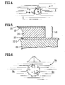
- Fig. 1 is a schematic illustration of an idealized cross-sectional view of an optical recording medium 1, understood as fabricated and operated generally along the lines of what is presently taught in the literature for tellurium (e.g., see Ash article).
- Medium 1 comprises a support 2 on which is provided an "anti-reflective" base AR and, on AR, an information layer ("absorber") 5.
- base AR comprises a "reflector" layer 3, on which a transmissive "spacer” layer 4 is laid.
- Layers 3 and 4 may be characterized as, respectively, primarily reflective and primarily transmissive at the contemplated read/write wavelength
- Layers 3, 4, 5 will be understood as providing a multi-layer, low-reflecting (anti-reflection) design over most the visible spectrum as known in the art (see Ash article).
- Support 2 preferably comprises a polished aluminum disk of the type presently used in digital magnetic recording for computer disk drives, coated with an organic smoothing (subbing) layer 2-S adapted to render a satisfactorily- smooth, flat surface for deposition of reflector layer 3.
- an organic smoothing (subbing) layer 2-S adapted to render a satisfactorily- smooth, flat surface for deposition of reflector layer 3.
- This will be understood as preferably comprising a 14" disk to be operated at about 1800 (to several thousand) rpm with good surface smoothness (e.g., order of less than 0.1 micrometer peak-to-peak).
- a radiation (laser) beam of prescribed energy and wavelength may be understood as applied to medium 1 from a laser source L, so as to establish a "pit” or like "deformation” on layer 5 as “writing” takes place (e.g., at site “v” shown in phantom). More particularly, it will be desired to use a 10 mW gaussian beam with diameter of 0.8 pm (i.e., 800 nm or 1/ ⁇ ) and scanning at 45 m/sec., to form a "pit” with a certain minimum length and width of 0.8 um (though not necessarily circular or other prescribed shape-this requirement is too stringent for conventional means however).
- surface reflectance on absorber 5 can be made “zero” or a selected value by adjusting absorber thickness and spacer thickness.
- a "tri-layer” being here understood as comprising a transparent spacer with absorber on one face and reflector on the other).
- the reflector film may be eliminated (e.g., in favour of a "dielectric mirror") and that spacer 4 may comprise other materials/structures (e.g., several layers of like material that is also more insulative thermally).
- the coating parameters here will be understood as selected to preferably provide an "anti-reflective" condition for the so-coated disk at the contemplated recording frequency when the write beam is focused on this absorber layer.
- Anti-Reflection Structures for Optical Recording by Bell and Spong, Journal of Quantum Electronics, Vol. QE 14, No. 7, July, 1978; and for general prior art, see exemplary articles; “Optical Disk Systems Emerge”, IEEE Spectrum by Bartolini, et al, August 1978, page 20; and “Optical Recording Media Review” by Bartolini, SPIE Proceedings, Vol. 123, 1977, page 2; “Optical Storage Materials and Methods", SPIE Proceedings, Vol. 177, Optical Information Storage, 1979, page 56].
- deposition proceeds by thermal evaporation until the reflectance of layer 5 reaches a predetermined reflectance level.
- this may be done empirically, or by continually monitoring the reflectance of the absorber film (e.g., on a witness-chip) as layer 5 is deposited (see deposition techniques described by Zech in his cited article) or by like suitable optical techniques for deposition-monitoring; or by other known methods, such as monitoring deposited mass or by electrical properties.
- the reflectivity of the record medium 1 will be understood as modified at each bit-site “v” by the radiation beam from write-laser L, so that, upon detection with a suitable means, the "void areas” v (i.e., "pits") may be distinguished as relatively “high reflectance spots” from the low reflectance "non-void” background surrounding them, as known in the art.
- U.S.-4,285,056 to Bell describes a like medium where information is recorded as "openings" in both the absorber and transmissive spacer layers, with the lengths of the openings and of the unexposed intervening areas being varied along a specific information track to convey frequency information.
- This patent also calls-out various materials (e.g., among them titanium, rhodium, platinum, gold, nickel, chromium, manganese and vanadium) to be deposited using standard evaporation or electron beam evaporation techniques.
- U.S. 4,183,094 to Keezer et al. calls for laser recording on Te-Ge-Se-S materials to yield "interference changes" without creating such pits.
- Tellurium is a "low melting point/poor conductivity" metal commonly preferred by workers because it is felt to exhibit superior sensitivity, thus minimizing required (threshold) laser write- power.
- Absorber layer 5 preferably comprises a relatively thin layer of tellurium which is vapour deposited (thermally evaporated) onto spacer layer 4 (on a relatively flat--:51/20 X-record surface thereof.
- the Te is so evaporated in a high vacuum preferably using a large batch coating chamber with corresponding large coating distances and "double-rotation" of substrate, etc. to better ensure uniformity-e.g., using a refractory metal boat for a source [1.2 m box type coating chamber used in Ash article]. All dust and stains on parts should be reduced to a strict minimum, using the most rigorous "Clean Room” techniques.
- Substrate 2 comprises a flat, aluminum plate polished to desirable flatness and coated with "subbing" 2-S to appropriate flatness to accommodate deposition of thin reflector layer 3 (high reflectivity over at least the "working portion" of the contemplated radiation spectrum).
- "subbing" 2-S to appropriate flatness to accommodate deposition of thin reflector layer 3 (high reflectivity over at least the "working portion" of the contemplated radiation spectrum).
- About 60-90 nm of aluminum prefer about 60 nm, vapour-deposited
- aluminum is not a perfect reflector, workers will recognize that in some cases one will substitute a "multi-layer dielectric stack" or the like.
- Spacer 4 is likewise deposited atop reflector 3.
- Spacer 4 is a dielectric material which is relatively transparent to the "working portion" of the laser spectrum.
- the tellurium absorber layer 5 will be understood as highly absorptive of the contemplated recording layer spectrum (e.g., typically 25% absorptive; 30% reflective; with about 45% of the beam energy transmitted (for tri-layer cancellation, must transmit more than reflect.
- absorptive layer 5 depends on that of spacer 4. Where transmitted light should be reduced, one may wish to increase spacer thickness (in N ⁇ /4 periods-also reducing heat- loss possibly).
- the intensity and time exposure of the focused Write-Beam will be understood as sufficient to so elevate the temperature of absorber layer 5 as to cause the indicated change in reflectivity (at v sites) giving the desired read-out quality, etc. (e.g., so that adequate contrast, S/N ratio-may be realized, as understood by workers in the art-cf. an exemplary S/N ratio of 40-50 dB (peak-to-peak signal vs. RMS noise) for a bandwidth of about 15 MHz.
- Such a spot may be read-out with means known in the art; e.g. with a similar laser at low power (e.g., above described laser at 3 mW), the increase in reflected energy received (at a suitable photo-detector) is observed to yield an output signal representing the recorded bits, these being readily distinguishable from background-this read-energy being insufficient to "erase” or disturb the so-recorded bits, of course.
- read-out a frequency f R where "pit-depth" introduces a phase change vs. light reflected at surface of Te such as to maximize contrast therewith].
- Te film of Example I will be found characterized by a rapid increase in overall optical transmission after such "aging”. This is presumably caused by a general oxidation of the metal as well as severe selected site-attack beginning at "defect sites” in the metal film, (cf. analogous test per MIL SPEC #810-B).
- Record 10 will be understood as comprising a support 12 on which an "anti-reflective" base 1-AR is laid (like AR in Fig. 1, preferably comprising a reflective layer 13, with a transmissive spacer layer 14 laid upon 13), with absorber film 15 placed atop substrate 1-AR (spacer 14 thereof).
- absorber 15 comprises a film of "gold material” comprising an “island layer” deposited to function as an absorber film (somewhat like the Te film in the "Te Example", e.g. in a somewhat similar process and by similar means).
- absorber thickness very close attention is paid, during deposition, to controlling absorber thickness so that it yields a prescribed minimal "Dark Mirror” reflectance R m (e.g., here 10% was chosen) as further described below.
- film 15 is formed to be discontinuous, being formed in an island configuration for optimal results, as shown in Fig. 11 (100,000xTe micrograph) and as described below.
- the underlying spacer layer 14, reflector layer 13 and substrate 13 are (at least functionally) overwise the same as in “Te Example”, and thus will be understood as functioning as a “tri-layer”, with absorber 15, as understood in the art (e.g. see cited references).
- gold absorber film 15 is preferably formed by vapour depositing a gold material on the surface of Si0 2 spacer 4 until (monitoring the well known "tri-layer” effects surface-reflectivity of 5 first drops to preselected value R m (10% reflectance here), taking care to render the "insular" configuration.
- Reflectance R m may, conveniently, be set at any desired value consistant with adequate "writing” and read-out. Here, about 10% was arbitrarily selected (minimum for proper focusing, etc.
- Absorber layer 15 thus comprises an extremely thin "island-deposit" of gold which is vapour-deposited (thermally evaporated) onto spacer layer 14 (i.e., on a relatively flat; e.g. 0.5 A record- surface thereof).
- spacer layer 14 i.e., on a relatively flat; e.g. 0.5 A record- surface thereof.
- R m minimum reflectance
- the "islands” are formed such that, when subjected to the described laser write-beam (633.8 nm, 10 mW for 40 n.sec. etc.), reflectance changes significantly: quite enough for adequate read-out (e.g., going from about 10% to about 25-55%-see below for detailed discussion of Results).
- the absorber film 15 is thus preferably vaccum deposited on spacer layer 14 using present preferred techniques (e.g., "pure" gold has been so deposited in large vacuum chamber at ⁇ 10 -6 ⁇ 10 -7 Torr., from a molybdenum boat which was resistance-heated-deposition rate was about .5-.1 nm/sec.).
- present preferred techniques e.g., "pure” gold has been so deposited in large vacuum chamber at ⁇ 10 -6 ⁇ 10 -7 Torr., from a molybdenum boat which was resistance-heated-deposition rate was about .5-.1 nm/sec.
- the silica layer 14 was, itself, likewise vapour-deposited before receiving the gold film 15. All substrates were cleaned according to present good practice for optical thin films.
- this may be done empirically, or by continually monitoring the surface-reflectance of a witness-chip while absorber film 15 is deposited until satisfactory "islands" appear and see deposition techniques described by Zech in his cited article, or by other known methods, such as monitoring deposited mass or electrical properties during deposition).
- Exemplary Gold Island Absorber Layer Record 10 was recorded-upon, read-out and evaluated, with its sensitivity, etc., measured, as in the "Te Example” (e.g., using an He-Ne laser system of the type mentioned).
- the so-written bit sites appear to be "agglomerate-holes" (where absorber has been made to “agglomerate” and where absorber material may also be caused to migrate toward the hole-periphery, or beyond)-this across a hole-diameter comparable to that of the read-beam (e.g., 1/4-3/4 thereof); to exhibit a like increase in reflectance and higher output signal.
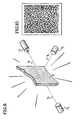
- Fig. 6 is an artistic rendering showing such an "agglomerate-hole” (or “quasi-pit") as seen in photo-micrographs of such records.
- an "agglomerate-hole” 15 P will be understood as a somewhat-circular written-spot, or physical- optical discontinuity in the virgin unwritten absorber film 15 " .
- Spot 15 P will be on the order of laser beam-diameter (e.g., 40-120% thereof) and may include a "rim” or partial-rim about its periphery.
- spots 15 P will be understood as constituting an "optical void” or discontinuity at the selected read-wavelength ( ⁇ w ); whereas the virgin island film 15v appears relatively continuous (partial) reflector.
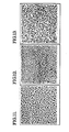
- Fig. 11 is a microscopic plan view (100,OOOxTe micrograph) of the original, virgin (i.e., unrecorded-upon) reflecting surface of an Au absorber film like that above-described. It will be evident this surface appears as a physically discontinuous, or partly discontinuous, "insular" configuration, exhibiting a fairly regular pattern (semi- islands on the Si0 2 spacer). For this Ex. I, the islands will be understood as having diameters on the order of a few tens nm (e.g., 10-30 nm typical), separated by intervals of comparable dimensions (e.g., 5-20 nm apart-vs. laser beam 500-10,000 nm wide; cf 632 nm wavelength). The virgin film 15 will thus exhibit a certain "% void" range (e.g., a few % to 10% voids).
- At least some of the first-order factors controlling such island formation are: absorber material, deposition-rate, adhesion; substrate material and condition (e.g., cleaning, roughness, etc.) and temperature; presence of "nucleation layer", presence of vapour-contaminants (vacuum pressure) and like factors as will be appreciated by workers. For example, too-cool a substrate will render a continuous film, but too-hot will leave no film at all.
- workers may compare Figs. 12 and 13 with referenced Fig. 11.
- Fig. 12 a similar film was prepared (like Ex. I) except that the silica substrate was coated with a bismuth oxide layer for nucleation as known in the art.
- Fig. 13 was similar, with a chromium nucleation layer instead. Compared with Fig. 11, Fig. 12 seemed to exhibit thinner islands farther apart, while Fig. 13 is a continuous gold film (no islands).
- the cited laser apparatus could not "write” at all on the film of Fig. 13 (at cited power level); while the film of Fig. 12 wrote like that of Fig. 11 (Ex. I) except for a bit lower sensitivity.
- the (evaporo-deposited) absorber constitutes gold plus a minor concentration of tin. This is laid-down as a laminate for convenience of deposition: first gold, then tin, then gold (alternatively, one can add other (% void low enough) so that absorber film 15 "appears” like a (relatively continuous) "optical reflector” at selected (R/W lasers).
- the write-bean is assumed, here, to so effect the islands in a bit-site as to cause "agglomeration" and the (usually) attendant increase in average island size and spacing (increased % void area).
- the initial (virgin) % void will be sufficient to accommodate a prescribed minimal heat loss, radially, yet not so large that initial reflectance (R o ) exceeds the desired "near zero" value (required for a "Dark Mirror").
- this writing operation may describe this writing operation as so energizing the absorber film as to, in effect, significantly separate absorber mass at the bit site.
- a "so-written" spot may shift these values to about 30%-10%-60%, respectively, for the subject write wavelength (tri-layer).
- the (evaporo-deposited) absorber constitutes gold plus a minor concentration of tin. This is laid-down as a laminate for convenience of deposition: first gold, then tin, then gold (alternatively, one can add other dual layers of tin and gold too). Upon heating, this "laminate" should inter-diffuse to form (mostly) a Au/Sn alloy (mostly gold, so "gold characteristics" should predominate).
- This Au/Sn film is substituted as the island-film of Ex. I (for 15 in Fig. 2) and is similarly written-upon. Effects: were qualitatively similar to Ex. I, while exhibiting greatly superior archivability and somewhat inferior sensitivity.
- Fig. 5 depicts a replication of Ex. I. (Fig. 2), except that a clear polymer is used as spacer (e.g., Teflon) and a tin-flash ("strike", as adhesion promoter, etc.) is interposed under the pure-gold absorber.
- spacer e.g., Teflon
- tin-flash tin-flash
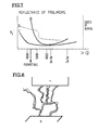
- Fig. 7 a plot of wavelength vs. reflectance (and index of refraction) virginal island filsm.
- a pure gold island absorber like that of Ex. I might exhibit a shift in refractive index as portrayed by curve A and a reflectance/X characteristics as in curve B. This obviously inhibits operating well above or below the He-Ne laser spectrum (633.8 nm-e.g., desired formatting of OD disks is not feasible at 440 nm, etc.; alternate use of Ga-As laser not feasible either).
- adding the Sn (island-) strike served to "flatten" the absorber's reflectivity curve as indicated at curve C. Workers will appreciated how significant such an increased radiation bandwidth can be.
- the polymer is quite heat-degradable; accordingly the deposition steps (for Sn, then Au) will keep within its temperature limits (-100°C) such gold films should be equal to the "archival conditions specified here. It is projected that such "gold records” can maintain adequate read-out (30+dB) for the order of ten (10) years under typical contemplated storage and use conditions.
- Ex. III is replicated, however adding a clear polymer supercoat on the absorber layer 15 as a protective overcoat.
- Ex. III is replicated except that a thin layer of Si0 2 is superposed on the polymer spacer 214 (Fig. 5), with the Sn strike deposited on the Si0 2 then the gold.
- Ex. III is replicated (Sn strike on polymer), except that an antimony "strike” follows the Sn strike, with gold deposited thereafter.
- the absorber film 15 (Fig. 2) comprises successive island-layers of: gold-lead-gold-lead- gold, each in proper island configuration. When heated, these island layers will readily inter-diffuse (distances so short) to form Au/Pb alloy- islands (Au major constituent, so ignore Pb properties as a first approximation, i.e. thus alloy will exhibit "gold characteristics" predominantly).
- film 15 is so deposited as a "laminate" for testing convenience, other methods will occur to workers.
- Sensitivity here was maximal; better than with pure gold (Ex. I) ⁇ e.g., approximately as “sensitive” as a tellurium absorber; often better, (e.g., about the sensitivity of "Te Example” has been measured). That is, information can be satisfactorily “written” on the gold-lead tri-layer here in the power regime of 5-15 mW/10-100 n.sec. (or 100-1000 p.J.). More specifically, about 5 mW for as little as 40 n.sec. is seen to "switch reflectivity". Some samples even "switch" in about 10-15 n.sec.
Landscapes
- Thermal Transfer Or Thermal Recording In General (AREA)
- Optical Record Carriers And Manufacture Thereof (AREA)
Claims (11)
Applications Claiming Priority (2)
| Application Number | Priority Date | Filing Date | Title |
|---|---|---|---|
| US38169482A | 1982-05-25 | 1982-05-25 | |
| US381694 | 1995-01-31 |
Publications (2)
| Publication Number | Publication Date |
|---|---|
| EP0096501A1 EP0096501A1 (de) | 1983-12-21 |
| EP0096501B1 true EP0096501B1 (de) | 1988-11-09 |
Family
ID=23506017
Family Applications (1)
| Application Number | Title | Priority Date | Filing Date |
|---|---|---|---|
| EP83302969A Expired EP0096501B1 (de) | 1982-05-25 | 1983-05-24 | Verfahren zur Wahrnehmung eines Feuers |
Country Status (3)
| Country | Link |
|---|---|
| EP (1) | EP0096501B1 (de) |
| DE (1) | DE3378434D1 (de) |
| WO (1) | WO1983004336A1 (de) |
Families Citing this family (2)
| Publication number | Priority date | Publication date | Assignee | Title |
|---|---|---|---|---|
| EP0139507B1 (de) * | 1983-10-11 | 1989-05-24 | Unisys Corporation | Aufzeichnungsschichten mit Inseln und deren Herstellung |
| WO1985002482A1 (en) * | 1983-12-02 | 1985-06-06 | Burroughs Corporation | Cost-reduced optical disk record |
Citations (7)
| Publication number | Priority date | Publication date | Assignee | Title |
|---|---|---|---|---|
| DE2943203A1 (de) * | 1978-10-25 | 1980-05-08 | Fuji Photo Film Co Ltd | Thermisches aufzeichnungsmaterial |
| GB2052731A (en) * | 1979-06-21 | 1981-01-28 | Spirig Ernst | Temperature responsive device |
| EP0023809A1 (de) * | 1979-07-27 | 1981-02-11 | Xerox Corporation | Optisches Aufzeichnungsmedium |
| US4252890A (en) * | 1968-08-26 | 1981-02-24 | Xerox Corporation | Imaging system which agglomerates particulate material |
| DE3003136A1 (de) * | 1980-01-29 | 1981-07-30 | Siemens AG, 1000 Berlin und 8000 München | Verfahren zum herstellen von thermisch stabilen, metallischen schichten |
| EP0079231A2 (de) * | 1981-11-09 | 1983-05-18 | Unisys Corporation | Optisches Aufzeichnungsverfahren zur digitalen Datenspeicherung für Archivzwecke |
| EP0083396A1 (de) * | 1981-12-31 | 1983-07-13 | International Business Machines Corporation | Optisches Speicherungsmedium |
Family Cites Families (9)
| Publication number | Priority date | Publication date | Assignee | Title |
|---|---|---|---|---|
| DE2522928C2 (de) * | 1974-05-25 | 1984-04-05 | Canon K.K., Tokyo | Aufzeichnungsträger, Verfahren zu dessen Herstellung und Aufzeichnungsverfahren |
| US4038663A (en) * | 1975-09-23 | 1977-07-26 | U.S. Philips Corporation | Method of writing information with a modulated radiation beam onto an information storage medium and information storage medium particularly adapted to the method |
| JPS5814318B2 (ja) * | 1978-06-26 | 1983-03-18 | 富士写真フイルム株式会社 | 熱的記録材料 |
| JPS5522961A (en) * | 1978-08-07 | 1980-02-19 | Fuji Photo Film Co Ltd | Thermal recording material |
| US4222071A (en) * | 1978-12-22 | 1980-09-09 | Rca Corporation | Sensitivity information record |
| FI58578C (fi) * | 1979-02-02 | 1981-03-10 | Vaasan Hoeyrymylly Oy | Foerfarande foer framstaellning av knaeckebroed eller dylikt |
| US4285056A (en) * | 1979-10-17 | 1981-08-18 | Rca Corporation | Replicable optical recording medium |
| GB2063103A (en) * | 1979-11-16 | 1981-06-03 | Gen Electric | Applying fluorocarbon polymer coatings |
| JPS6023037B2 (ja) * | 1980-03-18 | 1985-06-05 | 旭化成株式会社 | 情報記録部材 |
-
1983
- 1983-05-24 DE DE8383302969T patent/DE3378434D1/de not_active Expired
- 1983-05-24 EP EP83302969A patent/EP0096501B1/de not_active Expired
- 1983-05-25 WO PCT/US1983/000809 patent/WO1983004336A1/en not_active Ceased
Patent Citations (7)
| Publication number | Priority date | Publication date | Assignee | Title |
|---|---|---|---|---|
| US4252890A (en) * | 1968-08-26 | 1981-02-24 | Xerox Corporation | Imaging system which agglomerates particulate material |
| DE2943203A1 (de) * | 1978-10-25 | 1980-05-08 | Fuji Photo Film Co Ltd | Thermisches aufzeichnungsmaterial |
| GB2052731A (en) * | 1979-06-21 | 1981-01-28 | Spirig Ernst | Temperature responsive device |
| EP0023809A1 (de) * | 1979-07-27 | 1981-02-11 | Xerox Corporation | Optisches Aufzeichnungsmedium |
| DE3003136A1 (de) * | 1980-01-29 | 1981-07-30 | Siemens AG, 1000 Berlin und 8000 München | Verfahren zum herstellen von thermisch stabilen, metallischen schichten |
| EP0079231A2 (de) * | 1981-11-09 | 1983-05-18 | Unisys Corporation | Optisches Aufzeichnungsverfahren zur digitalen Datenspeicherung für Archivzwecke |
| EP0083396A1 (de) * | 1981-12-31 | 1983-07-13 | International Business Machines Corporation | Optisches Speicherungsmedium |
Non-Patent Citations (1)
| Title |
|---|
| IEEE Journal of Quantum electronics, Vol. QE 17, No. 1, Jan. 1981, pages 69-77 * |
Also Published As
| Publication number | Publication date |
|---|---|
| EP0096501A1 (de) | 1983-12-21 |
| DE3378434D1 (en) | 1988-12-15 |
| WO1983004336A1 (en) | 1983-12-08 |
Similar Documents
| Publication | Publication Date | Title |
|---|---|---|
| US4430659A (en) | Protuberant optical recording medium | |
| EP0092113B1 (de) | Optisches Speicherelement zur Verwendung in einem optischen Speichersystem sowie ein Verfahren zur Herstellung des Speicherelements | |
| US4470053A (en) | Protuberant optical recording medium | |
| EP0079231B1 (de) | Optisches Aufzeichnungsverfahren zur digitalen Datenspeicherung für Archivzwecke | |
| EP0096504B1 (de) | Goldhaltiger Aufzeichnungsfilm zur Speicherung digitaler Daten | |
| EP0096501B1 (de) | Verfahren zur Wahrnehmung eines Feuers | |
| EP0098045B1 (de) | Goldhaltiger Aufzeichnungsfilm zur Speicherung digitaler Daten unter Verwendung eines Schreiblasers mit geringer Leistung | |
| EP0098046B1 (de) | Aufzeichnungsfilm zur Speicherung digitaler Daten unter Verwendung eines Schreiblasers mit geringer Energie | |
| EP0097430B1 (de) | Verfahren zur Wahrnehmung eines Feuers | |
| EP0096503A2 (de) | Wärmeempfindlicher Filmschliesser | |
| EP0362901A2 (de) | Optisches Medium zur Aufzeichnung von digitalen Daten | |
| US5177732A (en) | Optical recording using an agglomerating recording medium which changes reflectivity upon recording | |
| EP0079229B1 (de) | Vorrichtung zur digitalen Datenspeicherung mittels Strahlung niedriger Energie auf für Archivzwecke geeigneten optischen Speichermedien | |
| EP0096502A1 (de) | Aufzeichnungsfilm mit Inseln zur Speicherung digitaler Daten unter Verwendung eines Schreiblasers mit niedriger Leistung | |
| EP0079741B1 (de) | Aufzeichnungsmedien für Archivszwecke mit verbesserter Informationsschicht und damit verbundenem Substrat | |
| EP0139507A1 (de) | Aufzeichnungsschichten mit Inseln und deren Herstellung | |
| EP0079230A2 (de) | Herstellung von Aufzeichnungsmedien zur digitalen Datenspeicherung für Archivzwecke | |
| EP0079233A2 (de) | Verfahren zum Datenaufzeichnen für Archivzwecke und zugehörige Medien | |
| EP0079232A2 (de) | System zum Datenaufzeichnen mittels Strahlung niedriger Energie für Archivzwecke und zugehörige Medien | |
| JPS59500991A (ja) | ディジタル・デ−タ・ストレ−ジに適したアイランド状の記録フィルム | |
| JPS59500438A (ja) | 低出力書込レ−ザを用いるディジタル・デ−タ・ストレ−ジに適した金記録保存フィルム | |
| JPS59500439A (ja) | 低出力書込レ−ザを用いるディジタル・デ−タ・ストレ−ジに適した記録保存フィルム | |
| JPS59500883A (ja) | 低出力書込レ−ザを用いるディジタル・デ−タ・ストレ−ジに適した金合金記録保存フィルム | |
| EP0189462A1 (de) | Optische speicherungsstruktur | |
| JPS59500886A (ja) | ディジタル・デ−タ・ストレ−ジに適した第1金の記録保存フィルム |
Legal Events
| Date | Code | Title | Description |
|---|---|---|---|
| PUAI | Public reference made under article 153(3) epc to a published international application that has entered the european phase |
Free format text: ORIGINAL CODE: 0009012 |
|
| 17P | Request for examination filed |
Effective date: 19830528 |
|
| AK | Designated contracting states |
Designated state(s): BE DE FR GB NL SE |
|
| RAP1 | Party data changed (applicant data changed or rights of an application transferred) |
Owner name: BURROUGHS CORPORATION (A DELAWARE CORPORATION) |
|
| RAP1 | Party data changed (applicant data changed or rights of an application transferred) |
Owner name: UNISYS CORPORATION |
|
| GRAA | (expected) grant |
Free format text: ORIGINAL CODE: 0009210 |
|
| AK | Designated contracting states |
Kind code of ref document: B1 Designated state(s): BE DE FR GB NL SE |
|
| REF | Corresponds to: |
Ref document number: 3378434 Country of ref document: DE Date of ref document: 19881215 |
|
| ET | Fr: translation filed | ||
| PLBE | No opposition filed within time limit |
Free format text: ORIGINAL CODE: 0009261 |
|
| STAA | Information on the status of an ep patent application or granted ep patent |
Free format text: STATUS: NO OPPOSITION FILED WITHIN TIME LIMIT |
|
| 26N | No opposition filed | ||
| PGFP | Annual fee paid to national office [announced via postgrant information from national office to epo] |
Ref country code: GB Payment date: 19900418 Year of fee payment: 8 |
|
| PGFP | Annual fee paid to national office [announced via postgrant information from national office to epo] |
Ref country code: SE Payment date: 19900430 Year of fee payment: 8 |
|
| PGFP | Annual fee paid to national office [announced via postgrant information from national office to epo] |
Ref country code: FR Payment date: 19900521 Year of fee payment: 8 |
|
| PGFP | Annual fee paid to national office [announced via postgrant information from national office to epo] |
Ref country code: DE Payment date: 19900525 Year of fee payment: 8 |
|
| PGFP | Annual fee paid to national office [announced via postgrant information from national office to epo] |
Ref country code: NL Payment date: 19900531 Year of fee payment: 8 |
|
| PGFP | Annual fee paid to national office [announced via postgrant information from national office to epo] |
Ref country code: BE Payment date: 19900718 Year of fee payment: 8 |
|
| PG25 | Lapsed in a contracting state [announced via postgrant information from national office to epo] |
Ref country code: GB Effective date: 19910524 |
|
| PG25 | Lapsed in a contracting state [announced via postgrant information from national office to epo] |
Ref country code: SE Effective date: 19910525 |
|
| PG25 | Lapsed in a contracting state [announced via postgrant information from national office to epo] |
Ref country code: BE Effective date: 19910531 |
|
| BERE | Be: lapsed |
Owner name: UNISYS CORP. Effective date: 19910531 |
|
| PG25 | Lapsed in a contracting state [announced via postgrant information from national office to epo] |
Ref country code: NL Effective date: 19911201 |
|
| NLV4 | Nl: lapsed or anulled due to non-payment of the annual fee | ||
| GBPC | Gb: european patent ceased through non-payment of renewal fee | ||
| PG25 | Lapsed in a contracting state [announced via postgrant information from national office to epo] |
Ref country code: FR Effective date: 19920131 |
|
| PG25 | Lapsed in a contracting state [announced via postgrant information from national office to epo] |
Ref country code: DE Effective date: 19920303 |
|
| REG | Reference to a national code |
Ref country code: FR Ref legal event code: ST |
|
| EUG | Se: european patent has lapsed |
Ref document number: 83302969.7 Effective date: 19911209 |