EP0096510B1 - Système de commande répondant en premier lieu aux signaux de calculateurs numériques - Google Patents
Système de commande répondant en premier lieu aux signaux de calculateurs numériques Download PDFInfo
- Publication number
- EP0096510B1 EP0096510B1 EP83303003A EP83303003A EP0096510B1 EP 0096510 B1 EP0096510 B1 EP 0096510B1 EP 83303003 A EP83303003 A EP 83303003A EP 83303003 A EP83303003 A EP 83303003A EP 0096510 B1 EP0096510 B1 EP 0096510B1
- Authority
- EP
- European Patent Office
- Prior art keywords
- signals
- computer
- responsive
- output signals
- computers
- Prior art date
- Legal status (The legal status is an assumption and is not a legal conclusion. Google has not performed a legal analysis and makes no representation as to the accuracy of the status listed.)
- Expired
Links
Images


Classifications
-
- G—PHYSICS
- G06—COMPUTING OR CALCULATING; COUNTING
- G06F—ELECTRIC DIGITAL DATA PROCESSING
- G06F11/00—Error detection; Error correction; Monitoring
- G06F11/07—Responding to the occurrence of a fault, e.g. fault tolerance
- G06F11/16—Error detection or correction of the data by redundancy in hardware
- G06F11/1629—Error detection by comparing the output of redundant processing systems
- G06F11/1633—Error detection by comparing the output of redundant processing systems using mutual exchange of the output between the redundant processing components
-
- G—PHYSICS
- G05—CONTROLLING; REGULATING
- G05B—CONTROL OR REGULATING SYSTEMS IN GENERAL; FUNCTIONAL ELEMENTS OF SUCH SYSTEMS; MONITORING OR TESTING ARRANGEMENTS FOR SUCH SYSTEMS OR ELEMENTS
- G05B9/00—Safety arrangements
- G05B9/02—Safety arrangements electric
- G05B9/03—Safety arrangements electric with multiple-channel loop, i.e. redundant control systems
-
- G—PHYSICS
- G06—COMPUTING OR CALCULATING; COUNTING
- G06F—ELECTRIC DIGITAL DATA PROCESSING
- G06F11/00—Error detection; Error correction; Monitoring
- G06F11/07—Responding to the occurrence of a fault, e.g. fault tolerance
- G06F11/16—Error detection or correction of the data by redundancy in hardware
- G06F11/18—Error detection or correction of the data by redundancy in hardware using passive fault-masking of the redundant circuits
- G06F11/187—Voting techniques
- G06F11/188—Voting techniques where exact match is not required
-
- G—PHYSICS
- G06—COMPUTING OR CALCULATING; COUNTING
- G06F—ELECTRIC DIGITAL DATA PROCESSING
- G06F11/00—Error detection; Error correction; Monitoring
- G06F11/07—Responding to the occurrence of a fault, e.g. fault tolerance
- G06F11/16—Error detection or correction of the data by redundancy in hardware
- G06F11/20—Error detection or correction of the data by redundancy in hardware using active fault-masking, e.g. by switching out faulty elements or by switching in spare elements
- G06F11/202—Error detection or correction of the data by redundancy in hardware using active fault-masking, e.g. by switching out faulty elements or by switching in spare elements where processing functionality is redundant
- G06F11/2023—Failover techniques
- G06F11/2025—Failover techniques using centralised failover control functionality
Definitions
- This invention relates to control systems in which control is primarily or wholly effected by signals from digital computers. Such systems are commonly referred to as “full authority” digital control systems.
- control activity is commonly regulated by a digital data processor which is itself responsive to sensed and/or desired operating conditions.
- the number of these operating conditions may be large, and each of the individual conditions may fall within substantial ranges of values.
- the combinations and sequences of the operating values will then be very large indeed, so that it will not be possible to test the system over the whole of the combined operating conditions which it may encounter in use.
- the problem is increased by the relative ease with which a digital control system may be reprogrammed, so that extensive tests carried out with the system under control of a superseded program will no longer be valid.
- control being transferred to a separate computing device.
- the separate device is a single additional computer which may be an analog computer.
- the additional device comprises both the aforesaid analog computer and a duplicated computer system, transfer of control to the analog computer or to the duplicate system being dependent on the nature of the fault detected.
- the present invention provides a control system having two digital computers each of which is capable of providing output control signals over a full range of input parameters, and in which the control signals from each computer are subject to rigorous checks. Specifically the invention provides that the output control signals from each digital computer is checked against a corresponding control signal provided by a separately-programmed dissimilar computer, and against a limit signal provided by a separately-programmed dissimilar computer. Additionally each limit signal is checked against a corresponding limit signal which is provided by a computer which is dissimilar and separately programmed from the computer providing the first- mentioned limit signal.
- the present invention provides a control system for an apparatus which is responsive to input control signals, the system comprising a computer arrangement for generating said control signals, said computer arrangement including first a second digital computers each of which is responsive to operating conditions of the apparatus for generating respective first and second output signals, said first and second computers having differing hardware and being independently programmed with differing control programs, the system being characterised by a third computer which is responsive to at least some of said operating conditions for generating third output signals, and in that a switching device for deriving said input control signals from said first and second output signals or from said third output signals, and further that said second and third computers respectively generate first and second limiting values for said first and second output signals respectively, said first and second computers also generating first and second indicating signals if either of said output signals exceeds its corresponding limiting value by a predetermined amount (D), said switching circuit being operable in one of its switched states to cause said input control signals to be derived from said first and second output signals and being responsive to either of said indicating signals to cause said input control signals to
- means for controlling operation of said first and second computers so that said first control program and said first limiter program operate concurrently and said second control program and said second limiter program operate concurrently, and so that said first and second programs are run alternately.
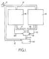
- the described embodiment relates to a control system for a gas turbine engine.
- the gas turbine engine 10 is responsive to analog control signals on a plurality of lines 11, and operating conditions of the engine 10, as for example compressor pressures, engine speeds and temperatures, and compressor temperatures are supplied from the engine 10 on a plurality of lines 12.
- the signals on lines 12 are combined with signals from an engine speed selector device 13 and are supplied on lines 14 to two digital computer arrangements 15,16, one of which is shown in more detail in Figure 2.
- Analog output signals from the arrangements 15, 16 are supplied on respective groups of lines 17, 18 to a switching device 19 of a known type.
- the device 19 is responsive to change-over signals on lines 20, 21 from the respective arrangements 15, 16, these signals being generated in a manner to be described hereafter.
- a block diagram of the arrangement 15 is shown in Figure 2 and comprises two computers 30, 31, each of which is responsive to the signals on lines 14.
- the computers 30, 31 are of different hardware designs and are independently programmed with respective distinct control programs which are responsive to the signals on lines 14 to provide nominally identical output control signals C1, C2 on lines 32, 33, respectively.
- the computers 30, 31 are also respectively programmed with distinct limiter programs which are also responsive to the signals on lines 14.
- Computer 31 generates limit signals L1 which define acceptable values for the signals on lines 32, for corresponding values of the signals on lines 14.
- the computer 30 generates limit signals L2 which define acceptable values for the signals on lines 33.
- the computers 30, 31 are under control of pulses 35 from a clock device 34, and the arrangement is such that the programs for the control signal C1 and for the limit signal L1 run concurrently, and are alternated with the programs for the signals C2, L2 which also run concurrently.
- Each program runs for 10 milliseconds on each occasion. In the present example this is effected by rendering the programs for signals C1, L1 responsive to a logic '1' from the device 34, and the programs for signals C2, L2 responsive to a logic '0' from the device 34.
- Instantaneous values of the signals C1 and L2 are supplied to the computer 31 on lines 36, and instantaneous values of the signals C2 or L1 are supplied to the computer 30 on lines 37.
- a first time interval T1 when the signal from the device 34 is at logic '1' the values C1, L1 are generated.
- the signal C1 is transferred on lines 36 to computer 31 and compared therein with the values of L1. If the value of C1 is greater than, or equal to, the value of L1, this may be symptomatic of a major system design fault, as for example an error in the system analysis, and a flag signal Fs1 is generated on a line 40.
- a previously stored value of signal L2 is also transferred on lines 36 to computer 31 and compared therein with the value of L1.
- a relatively small value d1 If the difference between these signals is greater than or equal to a relatively small value d1, this is likely to be symptomatic of a minor hardware or program fault, and a signal Fm1 is generated. Also during the time T1 a value C2 previously stored in the computer 31 is transferred on lines 37 to computer 30 and compared therein with the value of signal C1. If a difference between these latter values is greater than, or equal to, a relatively small value d2, this is likely to indicate a minor programming or hardware fault, and a signal Fm2 is generated.
- Signals Fs2, Fm3 and Fm4 are generated in response to fault conditions revealed by the respective comparisons during time T2.
- FIG. 3 indicates the layout of the computer 30.
- Computer 31 is generally similar but, as indicated above, has different hardware and is independently programmed.
- Computer 30 comprises a microprocessor (MPU) 50, two RAMs 51, 52, two ROMs 53, 54 and an input/output device 55, these elements being interconnected by an address and data bus 56 and by a control bus 57.
- the RAM 51 and ROM 53 are addressed only when the program for control signal C1 is running, and the RAM 52 and ROM 54 are addressed only when the program for the limit signal L2 is running. It is arranged that the most significant bit of address data for RAM 51 and ROM 53 is always logic '1' and that the corresponding bit of address data for RAM 52 and ROM 54 is always logic '0'. These address bits should therefore correspond to the signals on line 35 from the clock device 34, provided that the programs are running properly.
- the most significant bit currently on the address bus is supplied on a line 58 to an address monitor circuit 59, where it is compared with the signal on line 35.
- the monitor circuit 59 is shown in detail in Figure 4 and comprises a NOR gate 60 and an AND gate 61, both of which are responsive to the signals on lines 35, 58.
- a NOR gate 62 is responsive to the output states of the gates 60, 61. The arrangement is such that there is a logic '0' on an output line 63 from the gate 62 only when the logic states of the signals on lines 35, 58 are the same.
- the input/output device 55 is supplied with input data on lines 14 and with value of C2, L1 on lines 37 from the computer 31.
- Data lines from the bus 56 also communicate with a latching circuit 64 on which the flag signals FS2, Fm2 and Fm3 are held, is present.
- the aforesaid data lines also communicate a latching circuit 65 on which the control signal C1 is held to await validation as a result of the comparisons describad above.
- Latching circuit 65 also holds the signal C1 for passing on lines 36 to computer 31, for comparison with the value of C2 during time T2.
- the flag signal Fs2 indicative of a major system fault
- this signal is supplied from the latching circuit 64 on the line 43 to a change-over logic circuit 70 ( Figure 2), shown in more detail in Figure 5 and to be described hereafter.
- a change-over logic circuit 70 Figure 2
- the flag signals Fm2 or Fm3 are supplied by the latching circuit 64 on respective lines 71, 72 to an OR gate 73 ( Figure 3).
- the signal on line 63 from the monitor circuit 58 is also supplied to the OR gate 73.
- the arrangement is such that if either of signals Fm2 or Fm3 is present, or if the address on the bus 56 is not appropriate to the time T1 or T2 signalled by the clock device 34, a fault signal is provided on line 42 to the logic circuit 70.
- "Minor fault" signals corresponding to the signal on line 42, are supplied to the logic circuit 70 on a line 74 ( Figure 2) from the computer 31 in response to the presence of flag signals Fm1 or Fm4, or to an indication that an address within computer 31 is not appropriate to the time T1 or T2.
- the logic circuit 70 includes an OR gate 80 to which fault signals on the lines 40, 43 are applied.
- the gate 80 thus provides a fault signal on a line 81 in the presence of fault signals on either of lines 40, 43.
- An integrating circuit 82 of a known type is responsive to the signal on line 81 to provide an output signal on a line, 83, only if the signal on line 81 persists for more than a predetermined time.
- the circuit 70 also includes an OR gate 84 which is responsive to signals on the lines 42, 74.
- An integrating circuit 85 is responsive to an output signal from the gate 84 and provides a signal on the line 20 (see also Figures 1 and 2) if a fault indication signal from the gate 84 persists for more than a predetermined time.
- a NOR gate 86 is responsive to signals on lines 20, 83 to provide a signal on a line 87 only in the absence of a fault indication on line 20 or 83.
- the signal on line 87 is applied to the latching circuit 65 ( Figure 3) to allow the C1 value stored therein to be supplied on the lines 32, provided that the clock signal on line 35 also indicates time T1.
- the signal on line 87 is also applied to a corresponding latching circuit in the computer 31 to enable the C2 value to be supplied on lines 33 during time T2.
- the lines 32 and the lines 33 are both applied to a digital to analog converter 90, from which analog signals are supplied on the lines 17, by way of a selector switching circuit 91.
- a further computer 92 which may be an analog computer is responsive to selected ones of the input signals on lines 14, to provide control signals to the switching circuit 91, these signals being sufficient to effect safe control of the engine 10, even though this control may not provide optimum operating conditions. Operation of the switching circuit 91 in response to a fault indication of line 83 causes control signals on the lines 17 to be derived from the computer 92.
- the computer arrangement 16 is preferably identical in all respects to the arrangement 15.
- major design faults such as systems analysis faults are likely to be common to both of the arrangements 15, 16.
- a fault indication on the line 83 indicative of such a major fault, causes control of the engine 10 to revert to the computer 92.
- a fault indication on line 20, indicative of one of a number of minor hardware or software faults causes the switching device 19 ( Figure 1) to place the engine 10 under control of the computer arrangement 16.
Landscapes
- Engineering & Computer Science (AREA)
- Physics & Mathematics (AREA)
- General Physics & Mathematics (AREA)
- Theoretical Computer Science (AREA)
- Quality & Reliability (AREA)
- General Engineering & Computer Science (AREA)
- Automation & Control Theory (AREA)
- Safety Devices In Control Systems (AREA)
- Hardware Redundancy (AREA)
- Multi Processors (AREA)
Claims (8)
Applications Claiming Priority (2)
| Application Number | Priority Date | Filing Date | Title |
|---|---|---|---|
| GB8216234 | 1982-06-03 | ||
| GB8216234 | 1982-06-03 |
Publications (3)
| Publication Number | Publication Date |
|---|---|
| EP0096510A2 EP0096510A2 (fr) | 1983-12-21 |
| EP0096510A3 EP0096510A3 (en) | 1984-12-27 |
| EP0096510B1 true EP0096510B1 (fr) | 1988-07-27 |
Family
ID=10530829
Family Applications (1)
| Application Number | Title | Priority Date | Filing Date |
|---|---|---|---|
| EP83303003A Expired EP0096510B1 (fr) | 1982-06-03 | 1983-05-25 | Système de commande répondant en premier lieu aux signaux de calculateurs numériques |
Country Status (4)
| Country | Link |
|---|---|
| US (1) | US4590549A (fr) |
| EP (1) | EP0096510B1 (fr) |
| JP (1) | JPS5917658A (fr) |
| DE (1) | DE3377541D1 (fr) |
Families Citing this family (42)
| Publication number | Priority date | Publication date | Assignee | Title |
|---|---|---|---|---|
| US4622667A (en) * | 1984-11-27 | 1986-11-11 | Sperry Corporation | Digital fail operational automatic flight control system utilizing redundant dissimilar data processing |
| GB2172722B (en) * | 1985-03-22 | 1989-06-28 | United Technologies Corp | Backup control system (bucs) |
| AU568977B2 (en) * | 1985-05-10 | 1988-01-14 | Tandem Computers Inc. | Dual processor error detection system |
| US4799159A (en) * | 1985-05-30 | 1989-01-17 | Honeywell Inc. | Digital automatic flight control system with disparate function monitoring |
| DE3522418A1 (de) * | 1985-06-22 | 1987-01-02 | Standard Elektrik Lorenz Ag | Einrichtung zur meldung des belegungszustandes von gleisabschnitten im bereich eines stellwerks |
| GB2185951B (en) * | 1986-02-04 | 1989-07-05 | Rolls Royce | Helicopter rotor and engine control |
| US5701512A (en) * | 1986-03-11 | 1997-12-23 | Canon Kabushiki Kaisha | Data transmission control apparatus for system with input/output units used in common by several CPU's |
| US5297260A (en) * | 1986-03-12 | 1994-03-22 | Hitachi, Ltd. | Processor having a plurality of CPUS with one CPU being normally connected to common bus |
| US6379998B1 (en) * | 1986-03-12 | 2002-04-30 | Hitachi, Ltd. | Semiconductor device and method for fabricating the same |
| JPS62299435A (ja) * | 1986-06-19 | 1987-12-26 | Isuzu Motors Ltd | 異常検出装置付き車両の制御装置 |
| JPS6334298A (ja) * | 1986-07-28 | 1988-02-13 | Tokyo Keiki Co Ltd | 船舶用自動操舵装置 |
| US5128943A (en) * | 1986-10-24 | 1992-07-07 | United Technologies Corporation | Independent backup mode transfer and mechanism for digital control computers |
| DE3639065C2 (de) * | 1986-11-14 | 1997-01-09 | Bosch Gmbh Robert | Verfahren zur Überwachung eines rechnergesteuerte Stellglieder ansteuernden Prozeßrechners |
| JPH0616617B2 (ja) * | 1987-12-07 | 1994-03-02 | 富士通株式会社 | 初期条件設定方法 |
| GB8729901D0 (en) * | 1987-12-22 | 1988-02-03 | Lucas Ind Plc | Dual computer cross-checking system |
| US4890284A (en) * | 1988-02-22 | 1989-12-26 | United Technologies Corporation | Backup control system (BUCS) |
| JPH0721769B2 (ja) * | 1988-08-12 | 1995-03-08 | 日本電気株式会社 | マイクロプロセッサの冗長構成による機能監視方式 |
| GB2228114B (en) * | 1989-02-13 | 1993-02-10 | Westinghouse Brake & Signal | A system comprising a processor |
| DE3923432C2 (de) * | 1989-07-15 | 1997-07-17 | Bodenseewerk Geraetetech | Einrichtung zur Erzeugung von Meßsignalen mit einer Mehrzahl von Sensoren |
| JPH0747460B2 (ja) * | 1990-03-02 | 1995-05-24 | 株式会社日立製作所 | 乗客コンペアの制御装置 |
| US6247144B1 (en) * | 1991-01-31 | 2001-06-12 | Compaq Computer Corporation | Method and apparatus for comparing real time operation of object code compatible processors |
| DE4113959A1 (de) * | 1991-04-29 | 1992-11-05 | Kloeckner Humboldt Deutz Ag | Ueberwachungseinrichtung |
| US5434997A (en) * | 1992-10-02 | 1995-07-18 | Compaq Computer Corp. | Method and apparatus for testing and debugging a tightly coupled mirrored processing system |
| FR2704329B1 (fr) * | 1993-04-21 | 1995-07-13 | Csee Transport | Système de sécurité à microprocesseur, applicable notamment au domaine des transports ferroviaires. |
| EP0668552A1 (fr) * | 1994-02-18 | 1995-08-23 | Lucas Industries Public Limited Company | Dispositif de commande |
| JP3210833B2 (ja) * | 1995-05-09 | 2001-09-25 | 株式会社日立製作所 | エラーチェック方法および装置 |
| US5790791A (en) * | 1995-05-12 | 1998-08-04 | The Boeing Company | Apparatus for synchronizing flight management computers where only the computer chosen to be the master received pilot inputs and transfers the inputs to the spare |
| US5745539A (en) * | 1995-11-14 | 1998-04-28 | Westinghouse Electric Corporation | Apparatus and method for prioritization of multiple commands in an instrumentation and control system |
| WO1997018502A1 (fr) * | 1995-11-14 | 1997-05-22 | Westinghouse Electric Corporation | Dispositif et procede de mise en priorite d'instructions multiples dans un systeme d'instrumentation et de commande |
| US6199152B1 (en) * | 1996-08-22 | 2001-03-06 | Transmeta Corporation | Translated memory protection apparatus for an advanced microprocessor |
| US5905855A (en) * | 1997-02-28 | 1999-05-18 | Transmeta Corporation | Method and apparatus for correcting errors in computer systems |
| DE19743463A1 (de) * | 1997-10-01 | 1999-04-08 | Itt Mfg Enterprises Inc | Verfahren zur Fehlerkennung von Mikroprozessoren in Steuergeräten eines Kfz. |
| JP2001107751A (ja) | 1999-10-05 | 2001-04-17 | Honda Motor Co Ltd | 航空機用ガスタービン・エンジンの制御装置 |
| US6968469B1 (en) | 2000-06-16 | 2005-11-22 | Transmeta Corporation | System and method for preserving internal processor context when the processor is powered down and restoring the internal processor context when processor is restored |
| DE10125650B4 (de) * | 2001-05-25 | 2007-10-04 | Siemens Ag | Steuer-oder Regelverfahren |
| ES2297050T3 (es) * | 2001-09-24 | 2008-05-01 | Westinghouse Electric Company Llc | Modulo de interfaz para un componente controlado. |
| EP1296045A3 (fr) * | 2001-09-24 | 2004-07-14 | Goodrich Control Systems Limited | Commande éléctronique de moteur |
| EP1296046A3 (fr) * | 2001-09-24 | 2004-07-14 | Goodrich Control Systems Limited | Commande éléctronique de moteur |
| GB0225649D0 (en) * | 2002-11-04 | 2002-12-11 | Transitive Technologies Ltd | Incremental validation |
| JP4475593B2 (ja) * | 2003-11-19 | 2010-06-09 | 三菱電機株式会社 | エレベータ制御装置 |
| DE102005037242A1 (de) * | 2004-10-25 | 2007-02-15 | Robert Bosch Gmbh | Verfahren und Vorrichtung zur Umschaltung und zum Signalvergleich bei einem Rechnersystem mit wenigstens zwei Verarbeitungseinheiten |
| ES2328057T3 (es) * | 2006-05-16 | 2009-11-06 | Saab Ab | Sistema de control tolerante a fallos. |
Family Cites Families (12)
| Publication number | Priority date | Publication date | Assignee | Title |
|---|---|---|---|---|
| FR2162093B1 (fr) * | 1971-12-02 | 1977-04-08 | Hitachi Ltd | |
| JPS5831602B2 (ja) * | 1976-02-04 | 1983-07-07 | 株式会社日立製作所 | 二重系制御装置 |
| FR2344063A1 (fr) * | 1976-03-10 | 1977-10-07 | Smiths Industries Ltd | Circuit numerique de commande a deux voies au moins |
| DE2612100A1 (de) * | 1976-03-22 | 1977-10-06 | Siemens Ag | Digitale datenverarbeitungsanordnung, insbesondere fuer die eisenbahnsicherungstechnik |
| US4358823A (en) * | 1977-03-25 | 1982-11-09 | Trw, Inc. | Double redundant processor |
| US4151590A (en) * | 1977-11-15 | 1979-04-24 | Hokushin Electric Works, Ltd. | Process control system |
| DE2824168C3 (de) * | 1978-06-02 | 1985-11-14 | Standard Elektrik Lorenz Ag, 7000 Stuttgart | Einrichtung zur Steuerung von spurgebundenen Fahrzeugen im Zugverband |
| US4200226A (en) * | 1978-07-12 | 1980-04-29 | Euteco S.P.A. | Parallel multiprocessing system for an industrial plant |
| US4344128A (en) * | 1980-05-19 | 1982-08-10 | Frye Robert C | Automatic process control device |
| US4370706A (en) * | 1980-09-26 | 1983-01-25 | The Bendix Corporation | Controller for a dual servo system |
| GB2105492B (en) * | 1981-09-05 | 1985-03-06 | Lucas Ind Plc | A duplicated computer control system |
| US4504905A (en) * | 1981-09-05 | 1985-03-12 | Lucas Industries Plc | Digital control system including means for maintaining signals supplied thereby within limiting values |
-
1983
- 1983-05-25 EP EP83303003A patent/EP0096510B1/fr not_active Expired
- 1983-05-25 DE DE8383303003T patent/DE3377541D1/de not_active Expired
- 1983-05-27 US US06/498,860 patent/US4590549A/en not_active Expired - Fee Related
- 1983-06-01 JP JP58095905A patent/JPS5917658A/ja active Pending
Also Published As
| Publication number | Publication date |
|---|---|
| JPS5917658A (ja) | 1984-01-28 |
| EP0096510A2 (fr) | 1983-12-21 |
| EP0096510A3 (en) | 1984-12-27 |
| DE3377541D1 (en) | 1988-09-01 |
| US4590549A (en) | 1986-05-20 |
Similar Documents
| Publication | Publication Date | Title |
|---|---|---|
| US4590549A (en) | Control system primarily responsive to signals from digital computers | |
| GB1108540A (en) | Process back-up system | |
| US4665522A (en) | Multi-channel redundant processing systems | |
| CA2017227A1 (fr) | Reseau d'ordinateurs de controle en temps reel a detection et a contournement automatique des defaillances | |
| US5107425A (en) | Control system for control devices of a motor vehicle | |
| US3735356A (en) | Data processing arrangements having convertible majority decision voting | |
| US4222515A (en) | Parallel digital data processing system with automatic fault recognition utilizing sequential comparators having a delay element therein | |
| US4504905A (en) | Digital control system including means for maintaining signals supplied thereby within limiting values | |
| WO1999030528A3 (fr) | Terminaison redondante destinee a une localisation dynamique de defauts | |
| US5327362A (en) | System for detecting a runaway of a microcomputer | |
| US5077684A (en) | System for accurately informing each of adapters of its packaged location | |
| GB2237904A (en) | Digital control system | |
| GB2105492A (en) | A duplicated computer control system | |
| JPH0628003B2 (ja) | 多重化制御装置のデ−タ制御方法及び装置 | |
| JPS5413236A (en) | Bus control system | |
| GB2140583A (en) | Engine control systems | |
| SU1238245A1 (ru) | Самопровер емое устройство контрол кода | |
| JPS5657169A (en) | Programmable sequencer | |
| JPS6379121A (ja) | クロツク分配システム | |
| JPS5549760A (en) | Information processing unit diagnostic system | |
| JPS54103976A (en) | Logical circuit diagnoser | |
| JPH037961B2 (fr) | ||
| SU645160A2 (ru) | Устройство дл указани неисправности в дублированных дискретных автоматах | |
| JPS60219508A (ja) | 多重化検出装置 | |
| JPS5872226A (ja) | クロツク切替え回路 |
Legal Events
| Date | Code | Title | Description |
|---|---|---|---|
| PUAI | Public reference made under article 153(3) epc to a published international application that has entered the european phase |
Free format text: ORIGINAL CODE: 0009012 |
|
| AK | Designated contracting states |
Designated state(s): DE FR GB IT |
|
| PUAL | Search report despatched |
Free format text: ORIGINAL CODE: 0009013 |
|
| AK | Designated contracting states |
Designated state(s): DE FR GB IT |
|
| 17P | Request for examination filed |
Effective date: 19850403 |
|
| GRAA | (expected) grant |
Free format text: ORIGINAL CODE: 0009210 |
|
| AK | Designated contracting states |
Kind code of ref document: B1 Designated state(s): DE FR GB IT |
|
| PG25 | Lapsed in a contracting state [announced via postgrant information from national office to epo] |
Ref country code: IT Free format text: LAPSE BECAUSE OF FAILURE TO SUBMIT A TRANSLATION OF THE DESCRIPTION OR TO PAY THE FEE WITHIN THE PRESCRIBED TIME-LIMIT;WARNING: LAPSES OF ITALIAN PATENTS WITH EFFECTIVE DATE BEFORE 2007 MAY HAVE OCCURRED AT ANY TIME BEFORE 2007. THE CORRECT EFFECTIVE DATE MAY BE DIFFERENT FROM THE ONE RECORDED. Effective date: 19880727 Ref country code: FR Free format text: THE PATENT HAS BEEN ANNULLED BY A DECISION OF A NATIONAL AUTHORITY Effective date: 19880727 |
|
| REF | Corresponds to: |
Ref document number: 3377541 Country of ref document: DE Date of ref document: 19880901 |
|
| EN | Fr: translation not filed | ||
| PLBE | No opposition filed within time limit |
Free format text: ORIGINAL CODE: 0009261 |
|
| STAA | Information on the status of an ep patent application or granted ep patent |
Free format text: STATUS: NO OPPOSITION FILED WITHIN TIME LIMIT |
|
| 26N | No opposition filed | ||
| PG25 | Lapsed in a contracting state [announced via postgrant information from national office to epo] |
Ref country code: DE Effective date: 19900201 |
|
| PGFP | Annual fee paid to national office [announced via postgrant information from national office to epo] |
Ref country code: GB Payment date: 19960516 Year of fee payment: 14 |
|
| PG25 | Lapsed in a contracting state [announced via postgrant information from national office to epo] |
Ref country code: GB Effective date: 19970525 |
|
| GBPC | Gb: european patent ceased through non-payment of renewal fee |
Effective date: 19970525 |