EP0096701B1 - Circuit board fabrication leading to increased capacity - Google Patents
Circuit board fabrication leading to increased capacity Download PDFInfo
- Publication number
- EP0096701B1 EP0096701B1 EP83900226A EP83900226A EP0096701B1 EP 0096701 B1 EP0096701 B1 EP 0096701B1 EP 83900226 A EP83900226 A EP 83900226A EP 83900226 A EP83900226 A EP 83900226A EP 0096701 B1 EP0096701 B1 EP 0096701B1
- Authority
- EP
- European Patent Office
- Prior art keywords
- copper
- substrate
- pattern
- photoresist
- epoxy
- Prior art date
- Legal status (The legal status is an assumption and is not a legal conclusion. Google has not performed a legal analysis and makes no representation as to the accuracy of the status listed.)
- Expired
Links
- 238000004519 manufacturing process Methods 0.000 title description 6
- 239000000463 material Substances 0.000 claims description 69
- 239000000178 monomer Substances 0.000 claims description 21
- 229920001971 elastomer Polymers 0.000 claims description 18
- 239000005060 rubber Substances 0.000 claims description 18
- 239000004593 Epoxy Substances 0.000 claims description 17
- 239000002904 solvent Substances 0.000 claims description 16
- PSGCQDPCAWOCSH-UHFFFAOYSA-N (4,7,7-trimethyl-3-bicyclo[2.2.1]heptanyl) prop-2-enoate Chemical compound C1CC2(C)C(OC(=O)C=C)CC1C2(C)C PSGCQDPCAWOCSH-UHFFFAOYSA-N 0.000 claims description 7
- 239000011810 insulating material Substances 0.000 claims description 7
- NLHHRLWOUZZQLW-UHFFFAOYSA-N Acrylonitrile Chemical compound C=CC#N NLHHRLWOUZZQLW-UHFFFAOYSA-N 0.000 claims description 5
- 230000005670 electromagnetic radiation Effects 0.000 claims description 5
- KAKZBPTYRLMSJV-UHFFFAOYSA-N Butadiene Chemical compound C=CC=C KAKZBPTYRLMSJV-UHFFFAOYSA-N 0.000 claims description 4
- IISBACLAFKSPIT-UHFFFAOYSA-N bisphenol A Chemical compound C=1C=C(O)C=CC=1C(C)(C)C1=CC=C(O)C=C1 IISBACLAFKSPIT-UHFFFAOYSA-N 0.000 claims description 4
- GOXQRTZXKQZDDN-UHFFFAOYSA-N 2-Ethylhexyl acrylate Chemical compound CCCCC(CC)COC(=O)C=C GOXQRTZXKQZDDN-UHFFFAOYSA-N 0.000 claims description 3
- OMIGHNLMNHATMP-UHFFFAOYSA-N 2-hydroxyethyl prop-2-enoate Chemical compound OCCOC(=O)C=C OMIGHNLMNHATMP-UHFFFAOYSA-N 0.000 claims description 3
- 230000009477 glass transition Effects 0.000 claims description 3
- RSVDRWTUCMTKBV-UHFFFAOYSA-N sbb057044 Chemical compound C12CC=CC2C2CC(OCCOC(=O)C=C)C1C2 RSVDRWTUCMTKBV-UHFFFAOYSA-N 0.000 claims description 3
- 229920002554 vinyl polymer Polymers 0.000 claims description 3
- 239000004034 viscosity adjusting agent Substances 0.000 claims 3
- RYGMFSIKBFXOCR-UHFFFAOYSA-N Copper Chemical compound [Cu] RYGMFSIKBFXOCR-UHFFFAOYSA-N 0.000 description 81
- 229910052802 copper Inorganic materials 0.000 description 77
- 239000010949 copper Substances 0.000 description 77
- 239000000758 substrate Substances 0.000 description 54
- 238000000034 method Methods 0.000 description 40
- 239000000203 mixture Substances 0.000 description 29
- 229920002120 photoresistant polymer Polymers 0.000 description 26
- 230000008569 process Effects 0.000 description 16
- 239000004020 conductor Substances 0.000 description 14
- 238000000576 coating method Methods 0.000 description 13
- 239000011248 coating agent Substances 0.000 description 12
- 238000005530 etching Methods 0.000 description 12
- YMWUJEATGCHHMB-UHFFFAOYSA-N Dichloromethane Chemical compound ClCCl YMWUJEATGCHHMB-UHFFFAOYSA-N 0.000 description 9
- 238000000151 deposition Methods 0.000 description 9
- 238000007747 plating Methods 0.000 description 8
- 238000006243 chemical reaction Methods 0.000 description 7
- 238000011161 development Methods 0.000 description 7
- 229920001721 polyimide Polymers 0.000 description 7
- LYCAIKOWRPUZTN-UHFFFAOYSA-N Ethylene glycol Chemical compound OCCO LYCAIKOWRPUZTN-UHFFFAOYSA-N 0.000 description 6
- ZMXDDKWLCZADIW-UHFFFAOYSA-N N,N-Dimethylformamide Chemical compound CN(C)C=O ZMXDDKWLCZADIW-UHFFFAOYSA-N 0.000 description 6
- 239000004642 Polyimide Substances 0.000 description 6
- 239000000654 additive Substances 0.000 description 6
- ROOXNKNUYICQNP-UHFFFAOYSA-N ammonium persulfate Chemical compound [NH4+].[NH4+].[O-]S(=O)(=O)OOS([O-])(=O)=O ROOXNKNUYICQNP-UHFFFAOYSA-N 0.000 description 6
- -1 e.g. Substances 0.000 description 6
- 238000000059 patterning Methods 0.000 description 6
- 238000012545 processing Methods 0.000 description 6
- 150000001252 acrylic acid derivatives Chemical class 0.000 description 5
- 230000000996 additive effect Effects 0.000 description 5
- 230000008021 deposition Effects 0.000 description 5
- 229920000647 polyepoxide Polymers 0.000 description 5
- 239000000047 product Substances 0.000 description 5
- 230000005855 radiation Effects 0.000 description 5
- VEXZGXHMUGYJMC-UHFFFAOYSA-N Hydrochloric acid Chemical compound Cl VEXZGXHMUGYJMC-UHFFFAOYSA-N 0.000 description 4
- NIXOWILDQLNWCW-UHFFFAOYSA-M acrylate group Chemical group C(C=C)(=O)[O-] NIXOWILDQLNWCW-UHFFFAOYSA-M 0.000 description 4
- NIXOWILDQLNWCW-UHFFFAOYSA-N acrylic acid group Chemical group C(C=C)(=O)O NIXOWILDQLNWCW-UHFFFAOYSA-N 0.000 description 4
- 239000011324 bead Substances 0.000 description 4
- 238000007796 conventional method Methods 0.000 description 4
- 238000004132 cross linking Methods 0.000 description 4
- 238000005553 drilling Methods 0.000 description 4
- 238000009713 electroplating Methods 0.000 description 4
- 239000003822 epoxy resin Substances 0.000 description 4
- 238000007650 screen-printing Methods 0.000 description 4
- 230000008961 swelling Effects 0.000 description 4
- HEMHJVSKTPXQMS-UHFFFAOYSA-M Sodium hydroxide Chemical compound [OH-].[Na+] HEMHJVSKTPXQMS-UHFFFAOYSA-M 0.000 description 3
- ATJFFYVFTNAWJD-UHFFFAOYSA-N Tin Chemical compound [Sn] ATJFFYVFTNAWJD-UHFFFAOYSA-N 0.000 description 3
- 239000012190 activator Substances 0.000 description 3
- 229910001870 ammonium persulfate Inorganic materials 0.000 description 3
- 229940125904 compound 1 Drugs 0.000 description 3
- 150000001875 compounds Chemical class 0.000 description 3
- 238000005516 engineering process Methods 0.000 description 3
- 229910052751 metal Inorganic materials 0.000 description 3
- 239000002184 metal Substances 0.000 description 3
- 238000000206 photolithography Methods 0.000 description 3
- 239000004033 plastic Substances 0.000 description 3
- 229920003023 plastic Polymers 0.000 description 3
- 229920000642 polymer Polymers 0.000 description 3
- 229920005989 resin Polymers 0.000 description 3
- 239000011347 resin Substances 0.000 description 3
- 238000004544 sputter deposition Methods 0.000 description 3
- UOCLXMDMGBRAIB-UHFFFAOYSA-N 1,1,1-trichloroethane Chemical compound CC(Cl)(Cl)Cl UOCLXMDMGBRAIB-UHFFFAOYSA-N 0.000 description 2
- KWVGIHKZDCUPEU-UHFFFAOYSA-N 2,2-dimethoxy-2-phenylacetophenone Chemical compound C=1C=CC=CC=1C(OC)(OC)C(=O)C1=CC=CC=C1 KWVGIHKZDCUPEU-UHFFFAOYSA-N 0.000 description 2
- SMZOUWXMTYCWNB-UHFFFAOYSA-N 2-(2-methoxy-5-methylphenyl)ethanamine Chemical compound COC1=CC=C(C)C=C1CCN SMZOUWXMTYCWNB-UHFFFAOYSA-N 0.000 description 2
- NLGDWWCZQDIASO-UHFFFAOYSA-N 2-hydroxy-1-(7-oxabicyclo[4.1.0]hepta-1,3,5-trien-2-yl)-2-phenylethanone Chemical compound OC(C(=O)c1cccc2Oc12)c1ccccc1 NLGDWWCZQDIASO-UHFFFAOYSA-N 0.000 description 2
- BRLQWZUYTZBJKN-UHFFFAOYSA-N Epichlorohydrin Chemical compound ClCC1CO1 BRLQWZUYTZBJKN-UHFFFAOYSA-N 0.000 description 2
- 229920013646 Hycar Polymers 0.000 description 2
- 229920000459 Nitrile rubber Polymers 0.000 description 2
- KDLHZDBZIXYQEI-UHFFFAOYSA-N Palladium Chemical compound [Pd] KDLHZDBZIXYQEI-UHFFFAOYSA-N 0.000 description 2
- 239000002253 acid Substances 0.000 description 2
- PXKLMJQFEQBVLD-UHFFFAOYSA-N bisphenol F Chemical compound C1=CC(O)=CC=C1CC1=CC=C(O)C=C1 PXKLMJQFEQBVLD-UHFFFAOYSA-N 0.000 description 2
- NTXGQCSETZTARF-UHFFFAOYSA-N buta-1,3-diene;prop-2-enenitrile Chemical compound C=CC=C.C=CC#N NTXGQCSETZTARF-UHFFFAOYSA-N 0.000 description 2
- 230000008859 change Effects 0.000 description 2
- KRVSOGSZCMJSLX-UHFFFAOYSA-L chromic acid Substances O[Cr](O)(=O)=O KRVSOGSZCMJSLX-UHFFFAOYSA-L 0.000 description 2
- 229940125782 compound 2 Drugs 0.000 description 2
- 239000011889 copper foil Substances 0.000 description 2
- 238000007766 curtain coating Methods 0.000 description 2
- 230000000694 effects Effects 0.000 description 2
- 238000007772 electroless plating Methods 0.000 description 2
- AWJWCTOOIBYHON-UHFFFAOYSA-N furo[3,4-b]pyrazine-5,7-dione Chemical compound C1=CN=C2C(=O)OC(=O)C2=N1 AWJWCTOOIBYHON-UHFFFAOYSA-N 0.000 description 2
- 239000011521 glass Substances 0.000 description 2
- LNEPOXFFQSENCJ-UHFFFAOYSA-N haloperidol Chemical class C1CC(O)(C=2C=CC(Cl)=CC=2)CCN1CCCC(=O)C1=CC=C(F)C=C1 LNEPOXFFQSENCJ-UHFFFAOYSA-N 0.000 description 2
- 238000010438 heat treatment Methods 0.000 description 2
- 239000003999 initiator Substances 0.000 description 2
- QSHDDOUJBYECFT-UHFFFAOYSA-N mercury Chemical compound [Hg] QSHDDOUJBYECFT-UHFFFAOYSA-N 0.000 description 2
- 238000002156 mixing Methods 0.000 description 2
- 238000012986 modification Methods 0.000 description 2
- 230000004048 modification Effects 0.000 description 2
- 230000001737 promoting effect Effects 0.000 description 2
- KCTAWXVAICEBSD-UHFFFAOYSA-N prop-2-enoyloxy prop-2-eneperoxoate Chemical compound C=CC(=O)OOOC(=O)C=C KCTAWXVAICEBSD-UHFFFAOYSA-N 0.000 description 2
- 238000007761 roller coating Methods 0.000 description 2
- 238000007614 solvation Methods 0.000 description 2
- 239000000126 substance Substances 0.000 description 2
- LZDKZFUFMNSQCJ-UHFFFAOYSA-N 1,2-diethoxyethane Chemical compound CCOCCOCC LZDKZFUFMNSQCJ-UHFFFAOYSA-N 0.000 description 1
- DURPTKYDGMDSBL-UHFFFAOYSA-N 1-butoxybutane Chemical compound CCCCOCCCC DURPTKYDGMDSBL-UHFFFAOYSA-N 0.000 description 1
- PIZHFBODNLEQBL-UHFFFAOYSA-N 2,2-diethoxy-1-phenylethanone Chemical compound CCOC(OCC)C(=O)C1=CC=CC=C1 PIZHFBODNLEQBL-UHFFFAOYSA-N 0.000 description 1
- FPZWZCWUIYYYBU-UHFFFAOYSA-N 2-(2-ethoxyethoxy)ethyl acetate Chemical compound CCOCCOCCOC(C)=O FPZWZCWUIYYYBU-UHFFFAOYSA-N 0.000 description 1
- SBASXUCJHJRPEV-UHFFFAOYSA-N 2-(2-methoxyethoxy)ethanol Chemical compound COCCOCCO SBASXUCJHJRPEV-UHFFFAOYSA-N 0.000 description 1
- HRPVXLWXLXDGHG-UHFFFAOYSA-N Acrylamide Chemical group NC(=O)C=C HRPVXLWXLXDGHG-UHFFFAOYSA-N 0.000 description 1
- 229920002799 BoPET Polymers 0.000 description 1
- 229920013683 Celanese Polymers 0.000 description 1
- 239000005041 Mylar™ Substances 0.000 description 1
- 239000004677 Nylon Substances 0.000 description 1
- ISWSIDIOOBJBQZ-UHFFFAOYSA-N Phenol Chemical compound OC1=CC=CC=C1 ISWSIDIOOBJBQZ-UHFFFAOYSA-N 0.000 description 1
- 239000005062 Polybutadiene Substances 0.000 description 1
- VYPSYNLAJGMNEJ-UHFFFAOYSA-N Silicium dioxide Chemical compound O=[Si]=O VYPSYNLAJGMNEJ-UHFFFAOYSA-N 0.000 description 1
- VZTQQYMRXDUHDO-UHFFFAOYSA-N [2-hydroxy-3-[4-[2-[4-(2-hydroxy-3-prop-2-enoyloxypropoxy)phenyl]propan-2-yl]phenoxy]propyl] prop-2-enoate Chemical compound C=1C=C(OCC(O)COC(=O)C=C)C=CC=1C(C)(C)C1=CC=C(OCC(O)COC(=O)C=C)C=C1 VZTQQYMRXDUHDO-UHFFFAOYSA-N 0.000 description 1
- FHLPGTXWCFQMIU-UHFFFAOYSA-N [4-[2-(4-prop-2-enoyloxyphenyl)propan-2-yl]phenyl] prop-2-enoate Chemical class C=1C=C(OC(=O)C=C)C=CC=1C(C)(C)C1=CC=C(OC(=O)C=C)C=C1 FHLPGTXWCFQMIU-UHFFFAOYSA-N 0.000 description 1
- 230000002378 acidificating effect Effects 0.000 description 1
- 238000004026 adhesive bonding Methods 0.000 description 1
- 239000012670 alkaline solution Substances 0.000 description 1
- PNEYBMLMFCGWSK-UHFFFAOYSA-N aluminium oxide Inorganic materials [O-2].[O-2].[O-2].[Al+3].[Al+3] PNEYBMLMFCGWSK-UHFFFAOYSA-N 0.000 description 1
- 239000007864 aqueous solution Substances 0.000 description 1
- 230000015572 biosynthetic process Effects 0.000 description 1
- 229940106691 bisphenol a Drugs 0.000 description 1
- 230000003197 catalytic effect Effects 0.000 description 1
- 239000000919 ceramic Substances 0.000 description 1
- 239000003638 chemical reducing agent Substances 0.000 description 1
- 239000003086 colorant Substances 0.000 description 1
- 229920001577 copolymer Polymers 0.000 description 1
- 229910000365 copper sulfate Inorganic materials 0.000 description 1
- ARUVKPQLZAKDPS-UHFFFAOYSA-L copper(II) sulfate Chemical compound [Cu+2].[O-][S+2]([O-])([O-])[O-] ARUVKPQLZAKDPS-UHFFFAOYSA-L 0.000 description 1
- 238000005137 deposition process Methods 0.000 description 1
- 238000013461 design Methods 0.000 description 1
- 229940028356 diethylene glycol monobutyl ether Drugs 0.000 description 1
- 238000005868 electrolysis reaction Methods 0.000 description 1
- 125000003700 epoxy group Chemical group 0.000 description 1
- 230000008020 evaporation Effects 0.000 description 1
- 238000001704 evaporation Methods 0.000 description 1
- 239000004744 fabric Substances 0.000 description 1
- 239000000945 filler Substances 0.000 description 1
- 239000012467 final product Substances 0.000 description 1
- 229910021485 fumed silica Inorganic materials 0.000 description 1
- 238000007654 immersion Methods 0.000 description 1
- 230000000977 initiatory effect Effects 0.000 description 1
- 239000012212 insulator Substances 0.000 description 1
- 238000010030 laminating Methods 0.000 description 1
- 238000003475 lamination Methods 0.000 description 1
- 229910052753 mercury Inorganic materials 0.000 description 1
- 239000000615 nonconductor Substances 0.000 description 1
- 229920001778 nylon Polymers 0.000 description 1
- JCGNDDUYTRNOFT-UHFFFAOYSA-N oxolane-2,4-dione Chemical compound O=C1COC(=O)C1 JCGNDDUYTRNOFT-UHFFFAOYSA-N 0.000 description 1
- 229910052763 palladium Inorganic materials 0.000 description 1
- 239000000049 pigment Substances 0.000 description 1
- 229920002857 polybutadiene Polymers 0.000 description 1
- 239000009719 polyimide resin Substances 0.000 description 1
- 239000002243 precursor Substances 0.000 description 1
- 239000011253 protective coating Substances 0.000 description 1
- 230000009257 reactivity Effects 0.000 description 1
- 239000000243 solution Substances 0.000 description 1
- 239000010935 stainless steel Substances 0.000 description 1
- 229910001220 stainless steel Inorganic materials 0.000 description 1
- 238000003756 stirring Methods 0.000 description 1
- 238000012360 testing method Methods 0.000 description 1
- 238000002207 thermal evaporation Methods 0.000 description 1
- 230000009974 thixotropic effect Effects 0.000 description 1
- 229910001174 tin-lead alloy Inorganic materials 0.000 description 1
- 238000007740 vapor deposition Methods 0.000 description 1
- XLYOFNOQVPJJNP-UHFFFAOYSA-N water Substances O XLYOFNOQVPJJNP-UHFFFAOYSA-N 0.000 description 1
Images


Classifications
-
- H—ELECTRICITY
- H05—ELECTRIC TECHNIQUES NOT OTHERWISE PROVIDED FOR
- H05K—PRINTED CIRCUITS; CASINGS OR CONSTRUCTIONAL DETAILS OF ELECTRIC APPARATUS; MANUFACTURE OF ASSEMBLAGES OF ELECTRICAL COMPONENTS
- H05K3/00—Apparatus or processes for manufacturing printed circuits
- H05K3/46—Manufacturing multilayer circuits
- H05K3/4644—Manufacturing multilayer circuits by building the multilayer layer by layer, i.e. build-up multilayer circuits
- H05K3/4661—Adding a circuit layer by direct wet plating, e.g. electroless plating; insulating materials adapted therefor
-
- G—PHYSICS
- G03—PHOTOGRAPHY; CINEMATOGRAPHY; ANALOGOUS TECHNIQUES USING WAVES OTHER THAN OPTICAL WAVES; ELECTROGRAPHY; HOLOGRAPHY
- G03F—PHOTOMECHANICAL PRODUCTION OF TEXTURED OR PATTERNED SURFACES, e.g. FOR PRINTING, FOR PROCESSING OF SEMICONDUCTOR DEVICES; MATERIALS THEREFOR; ORIGINALS THEREFOR; APPARATUS SPECIALLY ADAPTED THEREFOR
- G03F7/00—Photomechanical, e.g. photolithographic, production of textured or patterned surfaces, e.g. printing surfaces; Materials therefor, e.g. comprising photoresists; Apparatus specially adapted therefor
- G03F7/0035—Multiple processes, e.g. applying a further resist layer on an already in a previously step, processed pattern or textured surface
-
- H—ELECTRICITY
- H05—ELECTRIC TECHNIQUES NOT OTHERWISE PROVIDED FOR
- H05K—PRINTED CIRCUITS; CASINGS OR CONSTRUCTIONAL DETAILS OF ELECTRIC APPARATUS; MANUFACTURE OF ASSEMBLAGES OF ELECTRICAL COMPONENTS
- H05K3/00—Apparatus or processes for manufacturing printed circuits
- H05K3/46—Manufacturing multilayer circuits
- H05K3/4644—Manufacturing multilayer circuits by building the multilayer layer by layer, i.e. build-up multilayer circuits
- H05K3/4673—Application methods or materials of intermediate insulating layers not specially adapted to any one of the previous methods of adding a circuit layer
- H05K3/4676—Single layer compositions
-
- H—ELECTRICITY
- H05—ELECTRIC TECHNIQUES NOT OTHERWISE PROVIDED FOR
- H05K—PRINTED CIRCUITS; CASINGS OR CONSTRUCTIONAL DETAILS OF ELECTRIC APPARATUS; MANUFACTURE OF ASSEMBLAGES OF ELECTRICAL COMPONENTS
- H05K2201/00—Indexing scheme relating to printed circuits covered by H05K1/00
- H05K2201/01—Dielectrics
- H05K2201/0104—Properties and characteristics in general
- H05K2201/0133—Elastomeric or compliant polymer
-
- H—ELECTRICITY
- H05—ELECTRIC TECHNIQUES NOT OTHERWISE PROVIDED FOR
- H05K—PRINTED CIRCUITS; CASINGS OR CONSTRUCTIONAL DETAILS OF ELECTRIC APPARATUS; MANUFACTURE OF ASSEMBLAGES OF ELECTRICAL COMPONENTS
- H05K2201/00—Indexing scheme relating to printed circuits covered by H05K1/00
- H05K2201/09—Shape and layout
- H05K2201/09209—Shape and layout details of conductors
- H05K2201/095—Conductive through-holes or vias
- H05K2201/09509—Blind vias, i.e. vias having one side closed
-
- H—ELECTRICITY
- H05—ELECTRIC TECHNIQUES NOT OTHERWISE PROVIDED FOR
- H05K—PRINTED CIRCUITS; CASINGS OR CONSTRUCTIONAL DETAILS OF ELECTRIC APPARATUS; MANUFACTURE OF ASSEMBLAGES OF ELECTRICAL COMPONENTS
- H05K3/00—Apparatus or processes for manufacturing printed circuits
- H05K3/0011—Working of insulating substrates or insulating layers
- H05K3/0017—Etching of the substrate by chemical or physical means
- H05K3/0023—Etching of the substrate by chemical or physical means by exposure and development of a photosensitive insulating layer
Definitions
- This invention relates to electronic circuitry and in particular to printed circuit board technology.
- Adjacent pattern lines must be deflected to avoid short circuits with the enlarged metallized portion surrounding the interconnection hole.
- the holes occupy a significant area and therefore increase the size of the printed circuit.
- these holes necessitate an increased complexity in the design of the printed circuit board pattern.
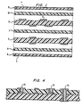
- printed circuit board patterns, 9, are formed on both major surfaces of two or more separate substrates (C-stages, 5, in FIG. 1).
- An adhesive bonding layer for example, an epoxy impregnated glass cloth, (B-stage, 7, in FIG. 1), is sandwiched between two or more substrates each having their associated copper patterns on both major surfaces.
- the multilevel configuration is completed by sandwiching the two C-stages and the intermediate B-stage between external layers which include a copper foil, 4, and an additional C-stage layer, 8 with their associated B-stage, 10. The entire structure is pressed together at an elevated temperature. The pressure and elevated temperature cures the B-stage resin and produces a monolithic structure.
- a multiple level circuit board has been developed that does not require the physical alignment of two independent substrates.
- a copper layer, 12, is deposited on a stainless steel carrier, 14.
- a photoresist is applied to the copper layer and imaged in the desired pattern so that the copper areas of the underlying layer forming the desired pattern (16) are covered and the remainder of the copper layer is exposed.
- the exposed copper is removed by etching and the photoresist is then removed leading to configuration 2B.
- a new photoresist layer is deposited and delineated so that holes, 17, in the resist, 13, are opened where connections between pattern levels are to be made. Copper is then evaporated onto the substrate over the resist and thus as a consequence, onto the exposed regions of the copper pattern leading to configuration, 2D.
- the photoresist is removed to leave the pattern, 18, with interconnection studs, 19 in configuration 2E.
- Polyimide resin is deposited onto the copper to yield configuration, 2F.
- the top of the polyimide is abraded to expose the copper structures, 19 in 2G.
- a photoresist is deposited onto the polyimide and suitably delineated to leave exposed areas of the polyimide where the second level copper pattern is to be formed leading to 2H. (This pattern includes the copper studs which are used as interconnection between the pattern levels.)
- a second copper layer is then deposited on the exposed polyimide and copper studs and the photoresist is removed leading to configuration 21. The steps are repeated to produce successive patterned layers.
- photolithography is again done by conventional techniques to delineate the desired interconnection openings, copper is evaporated onto the resist, the resist is removed, a second layer of polyimide is deposited, the surface of the polyimide is abraded to expose the copper, photolithography is employed to delineate the next pattern layer and copper is deposited onto the resist.
- FIG. 2 and the accompanying description a large number of processing steps are involved. Thus, a high-density printed circuit board that is producible in a nominal number of steps is not yet available.
- U.S. Patent 3,934,335 discloses a printed circuit arrangement in which electrically conducting patterns are printed on both sides of a substrate, in which a conductive via connects the patterns, and in which the patterns are insulated by an insulating material made from electromagnetic radiation sensitive material which has been radiated prior to formation of the patterns.
- a process, as shown in FIG. 3, employing a specific set of fabrication steps allows the manufacture of high-density multiple level printed circuit boards in a relatively small number of steps.
- the process is begun with a conventional substrate, 31, having a desired electrical conductor, e.g., copper, pattern, 32.
- An energy sensitive material i.e., a material such as a polymer precursor, which upon exposure to appropriate electromagnetic radiation undergoes a modification, e.g., a chemical change such as cross-linking which in turn modifies the mechanical and/or chemical properties of the material, is deposited on the substrate with its conductor pattern yielding configuration 3B. After its deposition, the energy sensitive material is patterned as shown at 3C.
- the energy sensitive material is then subjected to a blanket exposure of radiation, e.g., ultraviolet light, with an intensity significantly greater than that used for the initial delineation.
- radiation e.g., ultraviolet light
- a conductor e.g., copper
- the copper fills the voids in the energy sensitive material formed during the previous patterning steps and thus contacts the initial copper pattern. Additionally, the copper forms a layer on the energy sensitive material.
- a copper layer, 34 is presented for production of a second suitable patterned copper layer and interconnection, 35, between copper layers is provided.
- the desired pattern is formed in the newly deposited copper layers through conventional photolithography leading to configuration 3E.
- Suitable energy sensitive materials are those formed from a combination of (1) an acrylated epoxy resin (2) a vinyl- terminated rubber, e.g., a copolymer of acrylonitrile and butadiene, which is, in turn, terminated with acrylic acid moieties and (3) a suitable viscosity reducer, e.g., a monomer such as isobornyl acrylate or a solvent such as ethylene glycol.
- further pattern levels with the associated connection between levels are built by repeating the process, i.e., by sequentially depositing an appropriate energy sensitive material, delineating the material, if desired, blanket exposing the material, depositing the copper directly upon it and then forming the desired copper pattern.
- the printed circuit boards of the subject invention are typically built on a substrate having on its surface a delineated electrical conductor, e.g., copper, pattern.
- a delineated electrical conductor e.g., copper
- the substrate material employed and the method of producing the conductor pattern upon it is not critical.
- a substrate composed of glass-reinforced epoxy having a thickness generally in the range of 0.254 to 1.47 mm, a flexible circuit board, a ceramic, e.g., a 99 percent alumina material, or a circuit board having electrical conductor patterns on both major surfaces is utilized.
- the conductor pattern on the substrate is produced by conventional techniques, such as the subtractive, semiadditive, or fully additive deposition process.
- the subtractive, semiadditive and fully additive processes are described in C. F. Coombs, Jr., Printed Circuits Handbook,
- a copper layer having a thickness of approximately 7.6 to 76 mm is bonded to the surface of the substrate by a hot press lamination process.
- a photoresist such as Laminar LD dry-film photoresist, is then coated onto the copper layer.
- the photoresist is exposed and developed so that the areas of the copper that are to ultimately form the desired copper pattern remain covered.
- the portions of the copper layer that are not covered by the delineated photoresist are removed by etching leaving the desired copper pattern. After etching, the photoresist is solvated using materials such as methylene chloride.
- Both the additive and the semiadditive techniques require the deposition of a conductor such as copper on an insulator, e.g., a typical substrate.
- a conductor such as copper
- an insulator e.g., a typical substrate.
- electroless deposition it is generally necessary to use specific adherence promoting steps.
- the steps are conventional and typically include treatment with a solvent such as dimethyl formamide to swell the insulating material and treatment with an acid, e.g., chromic acid to etch the insulating material. It is also possible to achieve the desired adherence by using deposition techniques such as evaporation or sputtering.
- the semiadditive process includes the steps of initially promoting adhesion by, for example, swelling and etching the surface of the substrate by treating it with a solvent such as dimethyl formamide to produce swelling and a treatment, such as chromic acid, to produce etching.
- a layer of a conductive material such as copper, approximately 10 to 50 microinches thick, is then plated onto the substrate by electroless plating.
- electroless plating processes are fully described in literature references such as W. Goldie, Metallic Coating of Plastics, Electrochemical Publications (1968).
- the deposited conductive material layer e.g. the copper layer, is coated with a photoresist such as a Laminar LD dry-film photoresist (a proprietary product of Dynachem Company).
- the photoresist is patterned so that upon development only the areas of the copper plating which do not ultimately form the desired pattern are covered by the resist material.
- the thickness of the exposed copper portions is increased to a total thickness of approximately 7.6 to 76 mm by conventional electroplating.
- the photoresist is removed using a solvent such as methylene chloride.
- the entire copper surface is then exposed to an etchant such as ammonium persulfate for a period sufficient to remove the thin copper areas that were covered by the resist.
- the fully additive process in a typical embodiment, involves first treating the substrate to promote adhesion by a process described previously. The treated substrate is then subjected to catalytic palladium. (See Metallic Coating of Plastics, supra.) A photoresist is employed to cover the substrate and exposed so that upon development the areas of the substrate where the copper pattern is to be deposited are uncovered. The delineated substrate is then subjected to an electroless copper plating bath for periods typically on the order of 18 hours.
- this pattern is subsequently covered with an energy sensitive material to which, after patterning and upon appropriate processing, copper adheres.
- processing includes, for example, swelling and etching before the plating of a metal such as copper, through evaporative deposition, or through sputtering a metal such as copper, onto the energy sensitive material.
- the energy sensitive material is chosen so that upon irradiation with appropriately chosen electromagnetic radiation, the material in the irradiated region is less susceptible to removal, e.g., solvation, than the unirradiated regions.
- photosensitive materials are those including 1) an acrylated epoxy resin, 2) a low molecular weight rubber, e.g., a butadieneacrylonitrile based rubber, that has been terminated with at least one energy sensitive, e.g., photosensitive, moiety such as an acrylic acid moiety, and 3) a viscosity lowering component, e.g., a monomer or solvent.
- energy sensitive moiety is one that will undergo a reaction under the influence of suitable energy.
- composition (2) A variety of rubbers suitable for producing the desired rubber (composition (2)) are commercially available.
- exemplary of suitable rubbers is a butadieneacrylonitrile rubber having a terminal acrylate group, e.g.,
- HYCAR VTBN 1300X22 or VTBN 1300X23 sold by the B. F. Goodrich Company.
- Acrylated terminated rubbers having the structure are also useful. Such materials are described in U.S. patent 3,892,819.
- the rubber should have a molecular weight in the range 2,000 to 20,000, preferably 3,000 to 10,000. (Materials with lower molecular weights tend to shrink excessively while materials with higher molecular weight are generally too viscous to be handled easily.)
- the amount of acrylonitrile in the rubber be between 8 to 25 wt percent of the rubber. Higher or lower acrylonitrile content tends to produce materials which are less compatible with the epoxy composition (material (1)) and, thus although not precluded, generally are not desirable.
- Epoxy acrylates generally are prepared by reacting acrylic acid with an epoxy resin.
- Advantageous acrylated epoxy resins are those derived from bisphenol-A.
- the purpose of composition (1), i.e., the epoxy acrylate is to produce thermal stability in the final composition.
- Epoxy acrylates are producible by reacting a phenol such as bisphenol-A with epichlorohydrin and reacting the resultant product with acrylic acid.
- a phenol such as bisphenol-A
- epichlorohydrin reacting the resultant product with acrylic acid.
- epoxies produced by the reaction of bisphenol-F, with epichlorohydrin are suitable since they yield the desired Tg.
- composition (1) and composition (2) are cosolvated by a suitable solvent such as diethylene glycol monomethyl ether or diethylene glycol monoethyl ether acetate. If a solvent is employed, the solvent after coating is generally removed from the mixture by simply heating the mixture. However, the temperature used to remove the solvent should typically be less than 120 degrees C to avoid initiating a reaction in the photosensitive material.
- composition (3) Another means for reducing viscosity involves the use of a monomer that reacts under the influence of electromagnetic radiation with composition (1) and composition (2).
- a low viscosity (less than 200 centipoise) reactive monomer (composition (3)) is added primarily to bring these materials together into one water-clear phase and to reduce the viscosity of the entire composition to a manageable level.
- the molecular weight of the monomer should be typically less than 500.
- the monomer should have groups such as acrylate, acrylamide, or n-vinyl.
- the reactive groups are chosen so that they lead upon exposure to chain lengthening rather than cross-linking in the energy sensitive composition, i.e., they tend to extend the chain by linking the main backbone of the epoxy and rubber resins. If excessive cross-linking is initiated, it becomes difficult to promote adhesion to the material through swelling and etching.
- Monomers that satisfy these requirements include isobornyl acrylate (IBOA), hydroxyethyl acrylate (HEA), dicyclopentenyl oxyethyl acrylate (DOA), ethylhexyl acrylate (EHA), N-vinyl pyrollidone (NVP), and combinations of these monomers. (It should be noted that for certain applications a combination of solvent and monomer is useful for obtaining the desired viscosity. The exact combination for an advantageous viscosity is formulated by using a controlled sample.)
- the energy sensitive material is prepared by physically mixing the rubber (compound 2) with the modified epoxy acrylate (compound 1) and with a suitable viscosity control component (3).
- the mixture should contain between 10 and 30 wt percent, preferably between 20 and 25 wt percent of compound 2, between 25 and 45 wt percent, preferably between 30 and 40 wt percent, of compound 1, and the remainder monomer (3).
- a solvent is used instead of monomer (3) or in addition to it, the amount of this solvent is not critical. Sufficient solvent should be used to maintain viscosity at the appropriate level required for the particular coating application technique.
- additives such as colorants to produce a desired color, or fillers (e.g.
- fumed silica to enhance thixotropic properties, e.g., to yield a desired viscosity for applying the material to a substrate through screen printing.
- a photoinitiator such as benzoin ether
- Conventional photoinitiators such as benzoin ether, diethoxyacetophenone, or 2,2-dimethoxyphenylacetophenone are used to initiate the reaction in the acrylate photosensitive material and are added to the photosensitive material in a concentration of 1 to 5 wt percent.
- Monomer (3) has an effect on the ultimate properties of the polymer. Although viscosity is the most significant of these properties, other properties are also affected. For example, to a lesser extent the electrical properties, i.e., the resistance, and the glass transition temperature are affected. A resistance greater than 2 x 10 1 ohm for surface resistance and 4 x 10 8 ohm/cm for volume resistivity when tested by the ASTM D257 test, for the processed energy sensitive material is typically desirable to electrically isolate the various copper pattern levels.
- the viscosity of the energy sensitive material should not be so great that it is difficult to coat onto a substrate, i.e., viscosities in the range 100 to 100,000 centipoise are desirable for typical application techniques such as screen printing, roller coating or curtain coating.
- a suitable solvent or monomer should be employed to yield the desired viscosity for a particular application technique.
- the ambient temperature is above Tg adhesion of the photosensitive material to the underlying substrate is generally inadequate.
- the glass transition temperature should be above 50 degrees C, preferably above 75 degrees C.
- the epoxy chosen has the greatest effect on this property, generally monomers consistent with the desired Tg for the photosensitive mixture should be employed.
- a combination of suitable monomers are useful for producing properties not available by using a single monomer.
- IBOA yields excellent resistivity but also leads to a higher viscosity than other monomers.
- the energy sensitive material is coated onto it.
- Polymer thicknesses in the range 2 to 10 mils are typically employed: Thinner energy sensitive material layers lead to inadequate coverage and resistance, while thicker energy sensitive material layers typically produce inadequate resolution in the final pattern.
- the material is exposed by conventional techniques using actinic radiation in the desired pattern at a relatively low intensity level, e.g., 5 to 20 mW/ cm 2 for periods in the range 15 seconds to 2 min. In the preferred embodiment, the exposure is done so that the regions in the energy sensitive material to be removed leaving an opening or via is not exposed.
- the use of radiation in the wavelength range 250 to 350 nm for acrylate materials and their initiators yields upon development a configuration where the openings in the energy sensitive material leave uncovered areas in the underlying pattern to which interconnection between pattern layers are to be made. That is, as shown in FIG. 4, the interconnection, 41, is made through such openings.
- the initial substrate with its copper pattern is not shown in FIG. 4.
- the attainable hole size is typically 1 to 2 times the thickness of the energy sensitive material layer, extremely small holes, as compared to conventional printed circuit board technology, are attainable. There is no necessity for drilling holes to produce this interconnection and additionally, interconnection between several layers need not be made in a straight vertical configuration. (Configurations such as shown in FIG.
- development solvents such as 1,1,1-trichloroethane, ethylene glycol, or diethylene glycol monobutyl ether are employed.
- the surface and the openings, i.e., via holes, in the material are metallized by conventional techniques, e.g., swell and etch followed by electrolysis plating, vapor deposition or sputtering.
- a desired pattern is then produced on top of the cured resin in the cooper layer by techniques such as the previously described fully additive and semiadditive deposition procedure. The process of energy sensitive material deposition, photodelineation and copper pattern production upon the deposited material is repeated until the desired number of layers are obtained.
- a procedure for connecting any desired vertical pad to any desired horizontal pad of an array for mounting an integrated circuit was performed.
- a substrate having a pattern of copper on its surface was prepared by employing the subtractive method as described earlier with a "Laminar" (Registered Trade Mark) LD dry-film photoresist, and an etchant of 10 percent aqueous ammonium persulfate applied for 5 minutes.
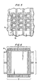
- the pattern produced in the copper by this subtractive procedure is shown in FIG. 6.
- the copper was treated with a hot (100 degrees C) alkaline solution ("Ebonol"(Registered Trade Mark) C from Enthone Company) which produced a black oxide on the copper surface.
- a photosensitive material and initiator was prepared for coating on the patterned substrate.
- a bead of the mixture was placed along the entire length of one edge of the patterned epoxy substrate.
- a three-quarter inch diameter, one-foot long threaded nylon rod having 40 threads per inch was employed to spread the bead of the mixture across the substrate This rod was placed behind the bead and drawn over the bead across the entire length of the substrate. This procedure left a coating of the mixture on the patterned substrate that had a thickness of approximately (5 mils) 0.127mm.
- a standard mylar mask having a pattern including circular openings was employed to expose the photosensitive coating. This exposure was performed by employing an HTG, model number 312-10, light source manufactured by Hybrid Techology Group, Inc. The intensity level of light in the 365 nm region reaching the surface of the substrate was approximately 20 mW/cm 2 . The exposure continued for approximately 15 seconds.
- the mask pattern was such that the series of holes or openings were opened through to each copper line, 61 (in FIGS. 5 and 6), from the points corresponding to the intersection of (A) the lines 55 of copper ultimately to be produced and to connect to pads 56 with (B) the copper lines, 61. Additionally, holes were opened to pads, 56 and 57.
- the substrate was suspended over a tank and was sprayed with diethylglycol monobutyl ether for approximately two and one-half minutes to develop the exposed substrate. (A Dupont model A, photoresist processor, was employed for this procedure).
- the substrate was rinsed in water for approximately 30 seconds and dried in a forced-air oven at 100 degrees C for 10 minutes.
- the substrate was then blanket cured using a 200 watt 2.54 cm (inch) high-pressure mercury vapor lamp light source positioned (6 inches) 15.24 cm from the substrate for an exposure time of approximately 15 seconds. This procedure yielded fully delineated holes as small as (6 mils) 152 pm in diameter.
- the substrate was immersed in 10 percent hydrochloric acid to dissolve the exposed black oxide.
- the substrate was then metallized by first immersing it in a 1 N sodium hydroxide bath for 1 minute at 30 degrees C to neutralize any residual acid from the etching bath.
- the substrate was then sequentially treated in a series of baths.
- the first bath employed was a 15 percent hydrochloric acid bath in which the substrate was immersed for 2 minutes at room temperature.
- the substrate was immersed in an activator (Enplate Activator 443 manufactured by Enthone Company) for 5 minutes at room temperature, in a post-activator (Enplate PA 491, a proprietary product of Enthone Company) for 10 minutes at room temperature and in an electroless copper plating solution (Enplate CU404, a proprietary product of the Enthone Company) for 8 minutes at room temperature.
- the treatment resulted in a copper layer thickness of approximately (20 microinches) .508 ⁇ m.
- the thickness of the copper was then increased by electroplating the substrate using a Sel-Rex CuBath M (a proprietary acidic copper sulfate plating bath of Oxy Metal Industries, Incorporated) at a current density of 269 Amps./M2 (25 Amps/ft 2 ) and a time of 50 minutes. (The electroplating was continued until the entire thickness of the copper layer from the top surface of the photosensitive material was (100 microinches) 2.54 um.
- Sel-Rex CuBath M a proprietary acidic copper sulfate plating bath of Oxy Metal Industries, Incorporated
- a (1.5 mil) 38.1 ⁇ m thick layer of "Laminar"@ LD dry-film photoresist was applied to the copper layer and exposed through a mask that included a series of (one-eighth inch) .317 cm wide opaque regions separated by (one-eighth inch) .317 cm wide transparent regions.
- Exposing radiation from an HTG model 312-10 light source with an intensity of approximately 20 mW/cm 2 at the photoresist surface was employed for approximately 15 seconds in a pattern to produce a series of lines, 55, with elbows, 70, in the resist emanating from the pads 56. (A magnification of a portion of three of these lines is shown in FIG. 5).
- the photoresist was then sprayed in a DuPont A resist processor with 1,1,1-trichloroethane for 30 seconds to develop the image.
- the copper uncovered by the development of the photoresist was increased in thickness by electroplating at a current density of 269 amps/m 2 (25 amps/ft 2 ) to a thickness of 25.4pm (1 mil).
- the surface of the copper was then tin plated using a Shipley LT-27 immersion tin bath to protect the copper surface during subsequent etching steps.
- the photoresist was then stripped employing methylene chloride, and the copper was etched with a 10 percent by weight aqueous solution of ammonium per sulfate until the thin areas of the copper were removed.
- the 90 degree peel strength of the copper strips was measured using a tensile strength pull tester.
- the tested peel strength was approximately 1074 to 1432 gm/cm (6 to 8 Ib/in) of width.
- a desirable adhesion for printed circuit boards is generally accepted to be 897 gm/cm. (5 Ib/in) or more.
- all the pads, 56 are connected to all the pads, 57.
- the desired elbow, 70, in the second copper pattern is removed by etching.
Landscapes
- Engineering & Computer Science (AREA)
- Manufacturing & Machinery (AREA)
- Microelectronics & Electronic Packaging (AREA)
- Physics & Mathematics (AREA)
- General Physics & Mathematics (AREA)
- Manufacturing Of Printed Circuit Boards (AREA)
- Production Of Multi-Layered Print Wiring Board (AREA)
- Manufacturing Of Printed Wiring (AREA)
- Photosensitive Polymer And Photoresist Processing (AREA)
- Electric Connection Of Electric Components To Printed Circuits (AREA)
Applications Claiming Priority (2)
| Application Number | Priority Date | Filing Date | Title |
|---|---|---|---|
| US33001181A | 1981-12-11 | 1981-12-11 | |
| US330011 | 1981-12-11 |
Publications (3)
| Publication Number | Publication Date |
|---|---|
| EP0096701A1 EP0096701A1 (en) | 1983-12-28 |
| EP0096701A4 EP0096701A4 (en) | 1987-04-28 |
| EP0096701B1 true EP0096701B1 (en) | 1989-08-30 |
Family
ID=23287944
Family Applications (1)
| Application Number | Title | Priority Date | Filing Date |
|---|---|---|---|
| EP83900226A Expired EP0096701B1 (en) | 1981-12-11 | 1982-11-22 | Circuit board fabrication leading to increased capacity |
Country Status (8)
| Country | Link |
|---|---|
| EP (1) | EP0096701B1 (it) |
| JP (1) | JPS58502079A (it) |
| CA (1) | CA1189630A (it) |
| DE (1) | DE3279915D1 (it) |
| ES (2) | ES518093A0 (it) |
| GB (1) | GB2111313B (it) |
| IT (1) | IT1195963B (it) |
| WO (1) | WO1983002172A1 (it) |
Families Citing this family (15)
| Publication number | Priority date | Publication date | Assignee | Title |
|---|---|---|---|---|
| US4566186A (en) * | 1984-06-29 | 1986-01-28 | Tektronix, Inc. | Multilayer interconnect circuitry using photoimageable dielectric |
| US4613560A (en) * | 1984-12-28 | 1986-09-23 | E. I. Du Pont De Nemours And Company | Photosensitive ceramic coating composition |
| US4915983A (en) * | 1985-06-10 | 1990-04-10 | The Foxboro Company | Multilayer circuit board fabrication process |
| EP0211180A3 (en) * | 1985-08-02 | 1989-08-09 | Shipley Company Inc. | Method for manufacture of multilayer circuit board |
| JPS6233135A (ja) * | 1985-08-06 | 1987-02-13 | Sanyo Kokusaku Pulp Co Ltd | 新規(メタ)アクリレート化合物 |
| EP0259784A3 (en) * | 1986-09-11 | 1988-10-12 | General Electric Company | Photo-imaged dielectric layer |
| DE3688255T2 (de) * | 1986-12-17 | 1993-07-22 | Foxboro Co | Verfahren zur herstellung von mehrschichtleiterplatten. |
| EP0281807B1 (de) * | 1987-03-09 | 1993-06-23 | Siemens Nixdorf Informationssysteme Aktiengesellschaft | Aufbautechnik für mehrlagige Verdrahtungen |
| EP0292219A3 (en) * | 1987-05-21 | 1989-10-11 | AT&T Corp. | Printed circuit board fabrication |
| DE3840207A1 (de) * | 1988-11-29 | 1990-05-31 | Draegerwerk Ag | Verfahren zur herstellung einer leiterplatte mit mehreren leiterbahnebenen und entsprechende multilayer-leiterplatte |
| US5362534A (en) * | 1993-08-23 | 1994-11-08 | Parlex Corporation | Multiple layer printed circuit boards and method of manufacture |
| AU2792395A (en) * | 1994-06-23 | 1996-01-19 | Hans-Jurgen Schafer | Method and device for coating printed-circuit boards, in particular for the manufacture of multi-chip-modules |
| TW277204B (it) * | 1994-12-02 | 1996-06-01 | Nippon Paint Co Ltd | |
| JP2000156564A (ja) * | 1998-11-20 | 2000-06-06 | Nec Corp | プリント配線板及びその製造方法 |
| CN107620388B (zh) * | 2017-09-21 | 2022-11-15 | 南京工业大学 | 木龙骨与面板的叠合橡胶连接结构 |
Family Cites Families (13)
| Publication number | Priority date | Publication date | Assignee | Title |
|---|---|---|---|---|
| US3269861A (en) * | 1963-06-21 | 1966-08-30 | Day Company | Method for electroless copper plating |
| US3615469A (en) * | 1969-06-02 | 1971-10-26 | Goodrich Co B F | Polymeric printing plates |
| US3649274A (en) * | 1969-09-18 | 1972-03-14 | Bunker Ramo | Coaxial circuit construction method |
| US3922479A (en) * | 1971-09-15 | 1975-11-25 | Bunker Ramo | Coaxial circuit construction and method of making |
| BE793030A (fr) * | 1971-12-20 | 1973-04-16 | Goodrich Co B F | Procede pour la realisation de matieres plastiques de resine epoxy |
| US3980483A (en) * | 1972-04-24 | 1976-09-14 | Nippon Oil Seal Industry Co., Ltd. | Photocurable composition |
| US3816281A (en) * | 1973-04-30 | 1974-06-11 | American Can Co | Poly(vinyl pyrrolidone)stabilized polymerized epoxy compositions and process for irradiating same |
| US3934335A (en) * | 1974-10-16 | 1976-01-27 | Texas Instruments Incorporated | Multilayer printed circuit board |
| GB2049972B (en) * | 1977-07-12 | 1982-06-23 | Asahi Chemical Ind | Photosensitive element for producing a printed circuit board |
| JPS5426471A (en) * | 1977-07-30 | 1979-02-28 | Matsushita Electric Works Ltd | Method of manufacturing multiilayer printed wiring board |
| US4157407A (en) * | 1978-02-13 | 1979-06-05 | E. I. Du Pont De Nemours And Company | Toning and solvent washout process for making conductive interconnections |
| US4225661A (en) * | 1978-05-10 | 1980-09-30 | The Richardson Company | Photoreactive coating compositions and photomechanical plates produced therewith |
| JPS5783094A (en) * | 1980-11-11 | 1982-05-24 | Nippon Telegraph & Telephone | Method of producing multilayer printed circuit board |
-
1982
- 1982-11-22 JP JP83500238A patent/JPS58502079A/ja active Pending
- 1982-11-22 WO PCT/US1982/001638 patent/WO1983002172A1/en not_active Ceased
- 1982-11-22 DE DE8383900226T patent/DE3279915D1/de not_active Expired
- 1982-11-22 EP EP83900226A patent/EP0096701B1/en not_active Expired
- 1982-12-03 GB GB08234589A patent/GB2111313B/en not_active Expired
- 1982-12-06 CA CA000417101A patent/CA1189630A/en not_active Expired
- 1982-12-10 IT IT24690/82A patent/IT1195963B/it active
- 1982-12-10 ES ES518093A patent/ES518093A0/es active Granted
-
1984
- 1984-02-15 ES ES529758A patent/ES8500700A1/es not_active Expired
Also Published As
| Publication number | Publication date |
|---|---|
| EP0096701A1 (en) | 1983-12-28 |
| IT8224690A0 (it) | 1982-12-10 |
| GB2111313B (en) | 1986-04-23 |
| WO1983002172A1 (en) | 1983-06-23 |
| ES529758A0 (es) | 1984-11-01 |
| ES8500700A1 (es) | 1984-11-01 |
| IT1195963B (it) | 1988-11-03 |
| EP0096701A4 (en) | 1987-04-28 |
| ES8404132A1 (es) | 1984-04-16 |
| ES518093A0 (es) | 1984-04-16 |
| JPS58502079A (ja) | 1983-12-01 |
| DE3279915D1 (en) | 1989-10-05 |
| GB2111313A (en) | 1983-06-29 |
| CA1189630A (en) | 1985-06-25 |
Similar Documents
| Publication | Publication Date | Title |
|---|---|---|
| US4511757A (en) | Circuit board fabrication leading to increased capacity | |
| US4888450A (en) | Circuit board fabrication leading to increased capacity | |
| EP0096701B1 (en) | Circuit board fabrication leading to increased capacity | |
| US4628022A (en) | Multilayer circuit board fabrication process and polymer insulator used therein | |
| US5544773A (en) | Method for making multilayer printed circuit board having blind holes and resin-coated copper foil used for the method | |
| US4360570A (en) | Use of photosensitive stratum to create through-hole connections in circuit boards | |
| US5509557A (en) | Depositing a conductive metal onto a substrate | |
| JPS61247090A (ja) | 半田スル−ホ−ルを有する回路板の製造方法 | |
| US4268614A (en) | Method of making printed circuit board | |
| US4795693A (en) | Multilayer circuit board fabrication process | |
| KR20010107703A (ko) | 엄격한 공차로 매입된 소자를 구비하는 인쇄 회로 기판형성 방법 | |
| EP0292219A2 (en) | Printed circuit board fabrication | |
| KR950003244B1 (ko) | 다층 회로판 제조공정 | |
| US6680440B1 (en) | Circuitized structures produced by the methods of electroless plating | |
| EP0623852B1 (en) | Resist compositions for circuit boards | |
| KR100199539B1 (ko) | 다층인쇄회로판을제조하는방법_ | |
| JPH10275983A (ja) | 多層プリント配線板 | |
| JPH0298995A (ja) | 多層配線板の製造方法 | |
| JP2571800B2 (ja) | 無電解めっき用感光性接着剤およびプリント配線板 | |
| CN114641136A (zh) | 电路板的铜层凸台制作方法及电路板 | |
| JP3298957B2 (ja) | 無電解めっき用接着剤シートとこの接着剤シートを用いたプリント配線板の製造方法およびプリント配線板 | |
| JP4759883B2 (ja) | 絶縁樹脂組成物及びこれを用いた多層配線板の製造方法 | |
| JPH07283540A (ja) | 多層プリント配線板およびその製造方法 | |
| JPH0756910B2 (ja) | スルーホール付配線板の製造方法 | |
| JPH07131182A (ja) | プリント回路板の製造方法 |
Legal Events
| Date | Code | Title | Description |
|---|---|---|---|
| PUAI | Public reference made under article 153(3) epc to a published international application that has entered the european phase |
Free format text: ORIGINAL CODE: 0009012 |
|
| AK | Designated contracting states |
Designated state(s): CH DE FR LI SE |
|
| 17P | Request for examination filed |
Effective date: 19831124 |
|
| A4 | Supplementary search report drawn up and despatched |
Effective date: 19870428 |
|
| 17Q | First examination report despatched |
Effective date: 19880129 |
|
| GRAA | (expected) grant |
Free format text: ORIGINAL CODE: 0009210 |
|
| AK | Designated contracting states |
Kind code of ref document: B1 Designated state(s): CH DE FR LI SE |
|
| REF | Corresponds to: |
Ref document number: 3279915 Country of ref document: DE Date of ref document: 19891005 |
|
| ET | Fr: translation filed | ||
| PLBE | No opposition filed within time limit |
Free format text: ORIGINAL CODE: 0009261 |
|
| STAA | Information on the status of an ep patent application or granted ep patent |
Free format text: STATUS: NO OPPOSITION FILED WITHIN TIME LIMIT |
|
| 26N | No opposition filed | ||
| EAL | Se: european patent in force in sweden |
Ref document number: 83900226.8 |
|
| PGFP | Annual fee paid to national office [announced via postgrant information from national office to epo] |
Ref country code: SE Payment date: 19990927 Year of fee payment: 18 Ref country code: CH Payment date: 19990927 Year of fee payment: 18 |
|
| PGFP | Annual fee paid to national office [announced via postgrant information from national office to epo] |
Ref country code: FR Payment date: 19991022 Year of fee payment: 18 |
|
| PGFP | Annual fee paid to national office [announced via postgrant information from national office to epo] |
Ref country code: DE Payment date: 19991231 Year of fee payment: 18 |
|
| PG25 | Lapsed in a contracting state [announced via postgrant information from national office to epo] |
Ref country code: SE Free format text: THE PATENT HAS BEEN ANNULLED BY A DECISION OF A NATIONAL AUTHORITY Effective date: 20001129 |
|
| PG25 | Lapsed in a contracting state [announced via postgrant information from national office to epo] |
Ref country code: LI Free format text: LAPSE BECAUSE OF NON-PAYMENT OF DUE FEES Effective date: 20001130 Ref country code: CH Free format text: LAPSE BECAUSE OF NON-PAYMENT OF DUE FEES Effective date: 20001130 |
|
| REG | Reference to a national code |
Ref country code: CH Ref legal event code: PL |
|
| EUG | Se: european patent has lapsed |
Ref document number: 83900226.8 |
|
| PG25 | Lapsed in a contracting state [announced via postgrant information from national office to epo] |
Ref country code: FR Free format text: LAPSE BECAUSE OF NON-PAYMENT OF DUE FEES Effective date: 20010731 |
|
| PG25 | Lapsed in a contracting state [announced via postgrant information from national office to epo] |
Ref country code: DE Free format text: LAPSE BECAUSE OF NON-PAYMENT OF DUE FEES Effective date: 20010801 |
|
| REG | Reference to a national code |
Ref country code: FR Ref legal event code: ST |