EP0097430A1 - Verfahren zur Wahrnehmung eines Feuers - Google Patents
Verfahren zur Wahrnehmung eines Feuers Download PDFInfo
- Publication number
- EP0097430A1 EP0097430A1 EP83302973A EP83302973A EP0097430A1 EP 0097430 A1 EP0097430 A1 EP 0097430A1 EP 83302973 A EP83302973 A EP 83302973A EP 83302973 A EP83302973 A EP 83302973A EP 0097430 A1 EP0097430 A1 EP 0097430A1
- Authority
- EP
- European Patent Office
- Prior art keywords
- absorber
- prescribed
- write
- medium
- island
- Prior art date
- Legal status (The legal status is an assumption and is not a legal conclusion. Google has not performed a legal analysis and makes no representation as to the accuracy of the status listed.)
- Granted
Links
Images


Classifications
-
- G—PHYSICS
- G11—INFORMATION STORAGE
- G11C—STATIC STORES
- G11C13/00—Digital stores characterised by the use of storage elements not covered by groups G11C11/00, G11C23/00, or G11C25/00
- G11C13/04—Digital stores characterised by the use of storage elements not covered by groups G11C11/00, G11C23/00, or G11C25/00 using optical elements ; using other beam accessed elements, e.g. electron or ion beam
- G11C13/048—Digital stores characterised by the use of storage elements not covered by groups G11C11/00, G11C23/00, or G11C25/00 using optical elements ; using other beam accessed elements, e.g. electron or ion beam using other optical storage elements
Definitions
- the present invention relates to a novel high density archival information storage medium, and more particularly to such a medium adapted for recording with low-power laser means.
- Optical storage of digital data is a relatively new technology, concerned with the storage and retrieval of digital information utilizing optical techniques, using a special related (ODD, "optical digital data") medium, such as an ODD disk.
- ODD optical digital data
- ODD disk optical digital data
- This disclosure relates to optical media and associated read/write techniques and apparatus which are adapted to record and read-back digital information using a focused beam of prescribed radiation energy, especially with low power laser equipment.
- a metal film as an "information layer" -- this layer to be softened, melted or vaporized (e.g., thermally-ablated) by a write-laser- beam so as to form a "void" (a pit, hole, bubble, etc., or other deformation) in the layer as the "bit".
- a metal film may be coated on the surface of a rotating disk.
- Tellurium has an attractively low (bulk-) melting point (about 450°C), conducts heat poorly and appears able to provide good sensitivity and S/N ratio; also, it is relatively convenient to deposit as a thin film. Bismuth is also commonly suggested for similar reasons. And related alloys (e.g., as Te-Ge, Te-As-Se and Bi-Se) have been suggested as of interest.
- Tellurium has been thought to exhibit a low write-threshold (energy) -- e.g., when compared with Aluminum -- as well as having a relatively low thermal diffusivity -- e.g., see U.S. 4,222,071 to Bell, et al; also see “Review of Optical Storage Media” by Zech, SPIE Vol. 177, Optical Information Storage, 1979, page 56 et sequ.; and also see “Optical Recording Media Review” by Bartolini, page 2 et sequ. of 1977 SPIE Vol. 123, "Optical Storage Materials and Methods".
- energy energy
- this Bartolini article discusses such absorber films ("Ablative Thin Films”) along with ten other optical recording means -- including "Photopolymers”, that is organic compounds known to undergo photochemical changes which involve a shift in refractive index.
- the Zech article discusses absorber films arranged and used so that with laser-writing a "pit" is developed in the absorber layer, this information being detected according to differential reflectivity (similarly for Bell patent).
- Extended archival stability is addressed by this invention which teaches the analogous use of absorber films of gold, etc. -- materials which are quite archival and are stable for extended use as computer information storage media, especially as for such optical data disk records for (as in Table I) computers.
- Another object is to teach such films exhibiting good sensitivity, adequate for low-power lasers; as well as extended archival life.
- a further object is to teach preparation of such records which are suitable for recording without need to"melt' the information layer; i.e., developing "altered reflectivity" bits (pits) while keeping the site well below its bulk melting temperature.
- base AR comprises a "reflector" layer 3, on which a transmissive "spacer” layer 4 is laid.
- Layers 3 and 4 may be characterized as, respectively, primarily-reflective and primarily transmissive at the contemplated read/write wavelengths.
- Layers 3, 4, 5 will be understood as providing a multi-layer, low- reflecting (anti-reflection) design over most of the visible spectrum as known in the art (see Ash article).
- Support 2 preferably comprises a polished aluminum disk of the type presently used in digital magnetic recording for computer disk drives, coated with an organic smoothing (subbing) layer 2-S adapted to render a satisfactorily-smooth, flat surface for deposition of reflector layer 3.
- an organic smoothing (subbing) layer 2-S adapted to render a satisfactorily-smooth, flat surface for deposition of reflector layer 3.
- a radiation (laser) beam of prescribed energy and wavelength may be understood as applied to medium 1 from a laser source L, so as to establish a "pit” or like "deformation” on layer 5 as “writing” takes place (e.g., at site “v” shown in phantom). More particularly, it will be desired to use a 10 mW gaussian beam with 0 diameter of 0.8 ⁇ m (i.e., 8000 A or 1/Z) and scanning at 45 m/sec., to form a "pit” with a certain minimum length and width of 0.8 pm (though not necessarily circular or other prescribed shape, -- this requirement is too stringent for conventional means however).
- surface reflectance (on absorber 5) can be made “zero” or a selected value by adjusting absorber thickness and spacer thickness.
- a "tri-layer” being here understood as comprising a transparent spacer with absorber on one face and reflector.on the other).
- the reflector film may be eliminated (e.g., in favor of a "dielectric mirror") and that spacer 4 may comprise other materials/structures (e.g., several layers of like material that is also more insulative thermally).
- the coating parameters here will be understood as selected to preferably provide an "anti-reflective" condition for the so-coated disk at the contemplated recording frequency when the write beam is focused on this absorber layer.
- Anti-Reflection Structures for Optical Recording by Bell and Spong, Journal of Quantum Electronics, Vol. QE 14, No. 7, July, 1978; and for general prior art, see exemplary articles: “Optical Disk Systems Emerge”, IEEE Spectrum by Bartolini, et al, August 1978, page 20; and “Optical Recording Media Review” by Bartolini, SPIE Proceedings, Vol. 123, 1977, page 2; “Optical Storage Materials and Methods", SPIE Proceedings, Vol. 177, Optical Information Storage, 1979, page 56].
- deposition proceeds by thermal evaporation until the reflectance of layer 5 reaches a predetermined reflectance level.
- this may be done empirically, or by continually monitoring the reflectance of the absorber film (e.g., on a witness-chip) as layer 5 is deposited (see deposition techniques described by Zech in his cited article) or by like suitable optical techniques for deposition-monitoring; or by other known methods, such as monitoring deposited mass or by electrical properties.
- the reflectivity of the record medium 1 will be understood as modified at each bit-site “v” by the radiation beam from write-laser L, so that, upon detection with a suitable means, the "void areas” v (i.e., "pits") may be distinguished as relatively “high reflectance spots” from the low reflectance "non-void” background surrounding them, as known in the art.
- U.S. 4,285,056 to Bell describes a like medium where information is recorded as "openings" in both the absorber and transmissive spacer layers, with the lengths of the openings and of the unexposed intervening areas being varied along a specific information track to convey frequency information.
- This patent also calls-out various materials (e.g., among them titanium, rhodium, platinum, gold, nickel, chromium, manganese and vanadium) to be deposited using standard evaporation or electron beam evaporation techniques.
- U.S. 4,183,094 to Keezer et al. calls for laser recording on Te-Ge-Se-S materials to yield "interference changes" without creating such pits.
- Tellurium is a "low melting point/poor conductivity" metal commonly preferred by workers because it is felt to exhibit superior sensitivity, thus minimizing required (threshold) laser write-power.
- Substrate 2 comprises a flat, aluminum plate polished to desirable flatness and coated with "subbing" 2-S to appropriate flatness to accommodate deposition of thin reflector layer 3 (high reflectivity over at least the "working portion" of the contemplated radiation 0 spectrum).
- About 600-900 A of aluminum prefer about 600 ⁇ , vapor-deposited has been found satisfactory. Since aluminum is not a perfect reflector, workers will recognize that in some cases one will substitute a "multi-layer dielectric stack" or the like.
- Spacer 4 is likewise deposited atop reflector 3.
- Spacer 4 is a dielectric material which is relatively transparent to the "working portion" of the laser spectrum.
- the tellurium absorber layer 5 will be understood as highly absorptive of the contemplated recording laser spectrum (e.g., typically 25% absorptive; 30% reflective; with about 45% of the beam energy transmitted (for tri-layer cancellation, must transmit more than reflect).
- absorptive layer 5 depends on that of spacer 4. Where transmitted light should be reduced, one may wish to increase spacer thickness (in N x X/4 periods -- also reducing heat-loss possibly).
- Te absorber 5 with its low melting point and a relatively short thermal diffusion length (poor conductivity) as a good, "high sensitivity” material which helps conserve incident laser energy.
- a write beam from laser source L falls upon site “v" of layer 5, a small portion of its energy will be reflected, a small portion absorbed and a large portion transmitted -- the transmitted portion being reflected back by layer 3 to be (principally) absorbed in layer 5.
- both incident and reflected energy will heat film 5, minimizing transmission losses (note: deposition of 5 yielded a "tri-layer”).
- Variations in absorber thickness or uniformity should be scrupulously avoided since this can reduce the write-energy coupled into the absorbing film and degrade sensitivity.
- the intensity and time exposure of the focused Write-Beam will be understood as sufficient to so elevate the temperature of absorber layer 5 as to cause the indicated change in reflectivity (at v sites) giving the desired read-out quality, etc. (e.g., so that adequate contrast, S/N ratio) may be realized, as understood by workers in the art, -- cf. an exemplary S/N ratio of 40-50 dB (peak-to-peak signal vs. RMS noise) for a bandwidth of about 15 MHz.
- pJ 10 -12 watt-sec. or Joules
- Such a spot may be read-out with means known in the art; e.g., with a similar laser at low power (e.g., above described laser at 3 mW), the increase in reflected energy received (at a suitable photo-detector) is observed to yield an output signal representing the recorded bits, these being readily distinguishable from background -this read-energy being insufficient to "erase” or disturb the so-recorded bits, of course.
- read-out at a frequency f R' where "pit-depth" introduces a phase change vs. light reflected at surface of Te such as to maximize contrast therewith].
- Te film of Example I will be found characterized by a rapid increase in overall optical transmission after such "aging". This is presumably caused by a general oxidation of the metal as well as severe selected site-attack beginning at "defect sites” in the metal film, (cf. analogous test per MIL SPEC #810-B).
- FIG. 2 shows an example I; absorber of gold material
- Record 10 will be understood as comprising a support 12 on which an "anti-reflective" base 1-AR is laid (like AR in FIG. 1, preferably comprising a reflective layer 13, with a transmissive spacer layer 14 laid upon 13), with absorber film 15 placed atop substrate 1-AR (spacer 14 thereof).
- absorber 15 comprises a film of "gold material” comprising an “island layer” deposited to function as an absorber film (somewhat like the Te film in the "Te Example", e.g. in a somewhat similar process and by similar means).
- absorber thickness very close attention is paid, during deposition, to controlling absorber thickness so that it yields a prescribed minimal "Dark Mirror” reflectance R m (e.g., here 10% was chosen) as further described below.
- film 15 is formed to be discontinuous, being formed in an island configuration for optimal results, as shown in FIG. 11 (100,000 x Te micrograph) and as described below.
- the underlying spacer layer 14, reflector layer 13 and substrate 12 are (at least functionally) otherwise the same as in “Te Example”, and thus will be understood as functioning as a “tri-layer”, with absorber 15, as understood in the art (e.g., see cited references).
- gold absorber film 15 is preferably formed by vapor depositing a gold material on the surface of SiO 2 spacer 4 until (monitoring the well known "tri-layer” effect) surface-reflectivity of 5 first drops to .
- preselected value R m (10% reflectance here), taking care to render the "insular" configuration.
- Reflectance R m may, conveniently, be set at any desired value consistant with adequate “writing” and read-out. Here, about 10% was arbitrarily selected (minimum for proper focusing, etc.
- the absorber film 15 is thus preferably vacuum deposited on spacer layer 14 using present preferred techniques (e.g., "pure" gold has been so deposited in large vacuum chamber at ⁇ 10 -6 - 10- 7 Torr., from a molybdenum boat which was resistance-heated -- deposition 0 rate was about 5-10 A/sec.).
- present preferred techniques e.g., "pure” gold has been so deposited in large vacuum chamber at ⁇ 10 -6 - 10- 7 Torr., from a molybdenum boat which was resistance-heated -- deposition 0 rate was about 5-10 A/sec.
- the silica layer 14 was, itself, likewise vapor-deposited before receiving the gold film 15. All substrates were cleaned according to present good practice for optical thin films.
- this may be done empirically, or by continually monitoring the surface-reflectance of a witness-chip while absorber film 15 is deposited until satisfactory "islands" appear (and see deposition techniques described by Zech in his cited article, or by other known methods, such as monitoring deposited mass or electrical properties during deposition).
- FIG. 6 is an artistic rendering showing such an "agglomerate-hole” (or “quasi-pit") as seen in photomicrographs of such records.
- an "agglomerate-hole” 15p will be understood as a somewhat-circular written-spot, or physical-optical discontinuity in the virgin unwritten absorber film 15 v .
- Spot 15 p will be on the order of laser beam-diameter (e.g., 40-120% thereof) and may include a "rim" or partial-rim about its periphery, Within the rim, relatively less absorber material is usually present; what there is will be seen as consolidated into absorber-globs gL, most of which are relatively large (e.g., usually fewer, many being larger than the tiny "islands” of virgin film 15 and FIG. 11, (and lie relatively farther apart). In effect, spots 15 will be understood as constituting an "optical void” or discontinuity at the selected read- wavelength ( ⁇ w); whereas the virgin island film 15 V appears as a relatively continuous (partial) reflector.
- At least some of the first-order factors controlling such island formation are: absorber material, deposition-rate, adhesion; substrate material and condition (e.g., cleaning, roughness, etc.) and temperature; presence of "nucleation layer", presence of vapor-contaminants (vacuum pressure) and like factors as will be appreciated by workers. For example, too-cool a substrate will render a continuous film, but too-hot will leave no film at all.
- workers may compare FIGS. 12 and 13 with referenced FIG. 11.
- a similar film was prepared (like Ex. I) except that the silica substrate was coated with a bismuth oxide layer for nucleation as known in the art.
- FIG. 13 was similar, with a chromium nucleation layer instead. Compared with FIG, 11, FIG. 12 seemed to exhibit thinner islands farther apart, while FIG. 13 is a continuous gold film (no islands).
- the cited laser apparatus could not "write” at all on the film of FIG. 13 (at cited power level); while the film of FIG. 12-wrote like that of FIG. 11 (Ex. I) except for a bit lower sensitivity.
- the write-beam is assumed, here, to so affect the islands in a bit-site as to cause "agglomeration" and the (usually) attendant increase in average island size and spacing (increased % void area).
- initial (virgin) % void will be sufficient to accommodate a prescribed minimal heat loss, radially, yet not so large that initial reflectance (R ) exceeds the desired linear zero" value (required for a "Dark Mirror").
- this writing operation may describe this writing operation as so energizing the absorber film as to, in effect, significantly separate absorber mass at the bit site.
- a "so-written" spot may shift these values to about 30% - 10% - 60%, respectively, for the subject write wavelength (tri-layer).
- the island configuration of the film may account for this apparently-reduced melting point, or it may trigger a write mechanism other than "gross melting" -- one is not yet sure.
- One theory is that such islands possess such high internal energy that relatively little write beam-energy can trigger their "bursting” and so agglomerating, yet without necessarily “melting them as such”.
- insular absorber films can be used to make OD disks as contemplated (e.g., satisfying all or most of the requirements of Table I).
- This Au/Sn film is substituted as the island-film of Ex. I (for 15 in FIG. 2) and is similarly written-upon. Effects: were qualitatively similar to Ex. I, while exhibiting greatly superior archivability and somewhat inferior sensitivity.
- FIG. 5 depicts a replication of Ex. I, (FIG. 2), except that a clear polymer is used as spacer (e.g., Teflon) and a tin-flash ("strike", as adhesion promotor, etc.) is interposed under the pure-gold absorber.
- spacer e.g., Teflon
- tin-flash e.g., adhesion promotor, etc.
- FIG. 7 a plot of wavelength vs. reflectance (and index of refraction) of virginal island films.
- a pure gold island absorber like that of Ex. I might exhibit a shift in refractive index as portrayed by curve A and a reflectance/X characteristic as in curve B. This obviously inhibits operating well above or below the 0 He-Ne laser spectrum (6338 A -- e.g., desired formatting of OD 0 disks is not feasible at 4400 A, etc.; alternate use of Ga-As laser not feasible either).
- adding the Sn (island-) strike served to "flatten" the absorber's reflectivity curve as indicated at curve C. Workers will appreciate how significant such an increased radiation bandwidth can be.
- the polymer is quite heat-degradable; accordingly the deposition steps (for Sn, then Au) will keep within its temperature limits ( ⁇ 100°C)
- Such gold films should be equal to the "archival” conditions specified here. It is projected that such "gold records” can maintain adequate read-out (30 + dB) for the order of ten (10) years under typical contemplated storage and use conditions.
- Ex. III is replicated except that a thin layer of SiO 2 is superposed on the polymer spacer 214 (FIG. 5), with the Sn strike deposited on the Si0 2 then the gold.
- FIG. 4 is an idealized showing of a typical "agglomerate-hole" written on such an Au/Sb absorber, the "virgin" island configuration v not shown here.
- Ex. III is replicated (Sn strike on polymer), except that an antimony "strike” follows the Sn strike, with gold deposited thereafter.
- the absorber film 15 (FIG. 2) comprises successive island-layers of: gold-lead-gold-lead-gold, each in proper island configuration. When heated, these island layers will readily inter-diffuse (distances so short) to form Au/Pb alloy-islands (Au major constituent, so ignore Pb properties as a first approximation, i.e. thus alloy will exhibit "gold characteristics" predominantly).
- film 15 is so deposited as a "laminate" for testing convenience, other methods will occur to workers.
- these filamentary peninsulae exhibit a much lower electrical resistance laterally (still quite high though) than the "islands" of Ex. I, etc. -- yet since they function similarly to write an "agglomerate-hole" it is assumed they retain much of the "thermal isolation" of the aforementioned "islands".
- such a filamentary configuration may also be characterized as “insular”. It records like the other "insular” films forming "agglomerate holes”.
- Sensitivity here was maximal; better than with pure gold (Ex. I) -- e.g'., approximately as “sensitive” as a tellurium absorber; often better, (e.g., about the sensitivity of "Te Example” has been measured). That is, information can be satisfactorily "written” on the gold-lead tri-layer here in the power regime of 5-15 mW/10-100 n.sec. (or 100-1000 p.J.). More specifically, about 5 mW for as little as 40 n.sec. is seen to "switch reflectivity". Some samples even "switch" in about 10-15 n.sec.
- one general teaching hereof is that, in fashioning OD disks with an absorber film in "tri-layer configuration" as described, one can achieve surprisingly good sensitivity by laying-down the absorber material in island form.
- noble metals like gold, palladium, etc. or their alloys may be so deposited as the absorber -- e.g., to enhance archival life while securing good sensitivity.
- an island-film absorber like gold can be combined with a co-constituent like lead or antimony (e.g., in a minor %) to enhance sensitivity, and/or with a co-constituent like tin to enhance archivability and optical characteristics (e.g., increased bandwidth).
- a co-constituent e.g., Au plus Pb or Pd plus Sn minimizes likelihood of "ejecta"; Au plus Sn and Sb to enhance S'y, A'y, bandpass and reduce ejecta.
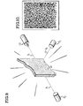
- FIG. 9 shows
- film ab is adapted to reflect most of beam b i (e.g., as reflect beam b r , toward a first detect unit D 1 ).
- film ab (beam-impacted portion thereof) is heated to pre-set level by LS (e.g., to agglomerate-temperature -- such as by a fire, flames nearby, etc.) it will agglomerate and "clarify" (relative to ⁇ i of b i -- so film ab now looks relatively transparent to ⁇ i ).
- LS e.g., to agglomerate-temperature -- such as by a fire, flames nearby, etc.
- source LS could be normally inactive, but upon first emitting energy, direct a portion (as beam b i ) to unit D 2 and thereby melt an aperture in film ab.
- beam b i could be scanned once across film ab to "write” a pattern therein -whereupon, with b i inactivated, a source of "backlighting illumination” could be projected at the entire "mask” so-etched (e.g., to generate a display or an optical printing plate). Workers will contemplate other like applications.
- Such island films may, in certain instances, be otherwise deposited, e.g., by other vapor-deposition techniques (vapor-deposition is very practical where, as in Ex. I, etc., it may also be used to deposit other related layers such as the reflector, spacer, etc.). Vapor co-deposition will usually be preferred for "alloys". Other methods may be feasible for depositing the absorber, such as sputtering. In any event, it will usually be preferred to monitor the film during deposition to closely control the deposited island configuration.
Landscapes
- Thermal Transfer Or Thermal Recording In General (AREA)
- Optical Record Carriers And Manufacture Thereof (AREA)
Applications Claiming Priority (2)
| Application Number | Priority Date | Filing Date | Title |
|---|---|---|---|
| US38169582A | 1982-05-25 | 1982-05-25 | |
| US381695 | 1982-05-25 |
Publications (2)
| Publication Number | Publication Date |
|---|---|
| EP0097430A1 true EP0097430A1 (de) | 1984-01-04 |
| EP0097430B1 EP0097430B1 (de) | 1988-07-20 |
Family
ID=23506020
Family Applications (1)
| Application Number | Title | Priority Date | Filing Date |
|---|---|---|---|
| EP83302973A Expired EP0097430B1 (de) | 1982-05-25 | 1983-05-24 | Verfahren zur Wahrnehmung eines Feuers |
Country Status (3)
| Country | Link |
|---|---|
| EP (1) | EP0097430B1 (de) |
| DE (1) | DE3377432D1 (de) |
| WO (1) | WO1983004338A1 (de) |
Cited By (1)
| Publication number | Priority date | Publication date | Assignee | Title |
|---|---|---|---|---|
| AT397736B (de) * | 1992-08-11 | 1994-06-27 | Aussenegg Franz Rembert Dr | Optisches datenspeichermedium |
Citations (5)
| Publication number | Priority date | Publication date | Assignee | Title |
|---|---|---|---|---|
| US2799600A (en) * | 1954-08-17 | 1957-07-16 | Noel W Scott | Method of producing electrically conducting transparent coatings on optical surfaces |
| US4222071A (en) * | 1978-12-22 | 1980-09-09 | Rca Corporation | Sensitivity information record |
| DE2941016A1 (de) * | 1979-10-10 | 1981-04-23 | William Vincent Windsor Ontario Youdelis | Verfahren zur erzeugung einer korrosionsfesten und harten oberflaeche an einem als gold bestht, sowie hierfuer geeignete zusammensetzungen |
| US4285056A (en) * | 1979-10-17 | 1981-08-18 | Rca Corporation | Replicable optical recording medium |
| AT365810B (de) * | 1977-04-05 | 1982-02-25 | Sony Corp | Scheibenfoermiges master-aufzeichnungsmedium fuer optische aufzeichnung |
Family Cites Families (8)
| Publication number | Priority date | Publication date | Assignee | Title |
|---|---|---|---|---|
| US4252890A (en) * | 1968-08-26 | 1981-02-24 | Xerox Corporation | Imaging system which agglomerates particulate material |
| FR2288370A1 (fr) * | 1974-10-18 | 1976-05-14 | Thomson Brandt | Perfectionnements aux supports d'information a lecture optique |
| US4313188A (en) * | 1976-03-19 | 1982-01-26 | Rca Corporation | Method of recording an ablative optical recording medium |
| JPS5528530A (en) * | 1978-08-17 | 1980-02-29 | Matsushita Electric Ind Co Ltd | Optical information recording method |
| JPS5557495A (en) * | 1978-10-25 | 1980-04-28 | Fuji Photo Film Co Ltd | Thermal recording medium |
| JPS5621893A (en) * | 1979-07-27 | 1981-02-28 | Xerox Corp | Optical recording part |
| WO1983001700A1 (en) * | 1981-11-09 | 1983-05-11 | Burroughs Corp | Deposition techniques for archival recording media for digital data storage |
| EP0083396A1 (de) * | 1981-12-31 | 1983-07-13 | International Business Machines Corporation | Optisches Speicherungsmedium |
-
1983
- 1983-05-24 DE DE8383302973T patent/DE3377432D1/de not_active Expired
- 1983-05-24 EP EP83302973A patent/EP0097430B1/de not_active Expired
- 1983-05-25 WO PCT/US1983/000806 patent/WO1983004338A1/en not_active Ceased
Patent Citations (5)
| Publication number | Priority date | Publication date | Assignee | Title |
|---|---|---|---|---|
| US2799600A (en) * | 1954-08-17 | 1957-07-16 | Noel W Scott | Method of producing electrically conducting transparent coatings on optical surfaces |
| AT365810B (de) * | 1977-04-05 | 1982-02-25 | Sony Corp | Scheibenfoermiges master-aufzeichnungsmedium fuer optische aufzeichnung |
| US4222071A (en) * | 1978-12-22 | 1980-09-09 | Rca Corporation | Sensitivity information record |
| DE2941016A1 (de) * | 1979-10-10 | 1981-04-23 | William Vincent Windsor Ontario Youdelis | Verfahren zur erzeugung einer korrosionsfesten und harten oberflaeche an einem als gold bestht, sowie hierfuer geeignete zusammensetzungen |
| US4285056A (en) * | 1979-10-17 | 1981-08-18 | Rca Corporation | Replicable optical recording medium |
Cited By (1)
| Publication number | Priority date | Publication date | Assignee | Title |
|---|---|---|---|---|
| AT397736B (de) * | 1992-08-11 | 1994-06-27 | Aussenegg Franz Rembert Dr | Optisches datenspeichermedium |
Also Published As
| Publication number | Publication date |
|---|---|
| DE3377432D1 (en) | 1988-08-25 |
| EP0097430B1 (de) | 1988-07-20 |
| WO1983004338A1 (en) | 1983-12-08 |
Similar Documents
| Publication | Publication Date | Title |
|---|---|---|
| EP0092113B1 (de) | Optisches Speicherelement zur Verwendung in einem optischen Speichersystem sowie ein Verfahren zur Herstellung des Speicherelements | |
| US4470053A (en) | Protuberant optical recording medium | |
| EP0079231B1 (de) | Optisches Aufzeichnungsverfahren zur digitalen Datenspeicherung für Archivzwecke | |
| EP0096504A1 (de) | Goldhaltiger Aufzeichnungsfilm zur Speicherung digitaler Daten | |
| EP0098046B1 (de) | Aufzeichnungsfilm zur Speicherung digitaler Daten unter Verwendung eines Schreiblasers mit geringer Energie | |
| EP0098045B1 (de) | Goldhaltiger Aufzeichnungsfilm zur Speicherung digitaler Daten unter Verwendung eines Schreiblasers mit geringer Leistung | |
| EP0096501A1 (de) | Verfahren zur Wahrnehmung eines Feuers | |
| EP0096503A2 (de) | Wärmeempfindlicher Filmschliesser | |
| EP0097430A1 (de) | Verfahren zur Wahrnehmung eines Feuers | |
| US5177732A (en) | Optical recording using an agglomerating recording medium which changes reflectivity upon recording | |
| EP0096502A1 (de) | Aufzeichnungsfilm mit Inseln zur Speicherung digitaler Daten unter Verwendung eines Schreiblasers mit niedriger Leistung | |
| EP0362901A2 (de) | Optisches Medium zur Aufzeichnung von digitalen Daten | |
| EP0079229B1 (de) | Vorrichtung zur digitalen Datenspeicherung mittels Strahlung niedriger Energie auf für Archivzwecke geeigneten optischen Speichermedien | |
| EP0079741B1 (de) | Aufzeichnungsmedien für Archivszwecke mit verbesserter Informationsschicht und damit verbundenem Substrat | |
| EP0079230A2 (de) | Herstellung von Aufzeichnungsmedien zur digitalen Datenspeicherung für Archivzwecke | |
| EP0079232A2 (de) | System zum Datenaufzeichnen mittels Strahlung niedriger Energie für Archivzwecke und zugehörige Medien | |
| EP0079233A2 (de) | Verfahren zum Datenaufzeichnen für Archivzwecke und zugehörige Medien | |
| EP0139507A1 (de) | Aufzeichnungsschichten mit Inseln und deren Herstellung | |
| JPS59500438A (ja) | 低出力書込レ−ザを用いるディジタル・デ−タ・ストレ−ジに適した金記録保存フィルム | |
| JPS59500439A (ja) | 低出力書込レ−ザを用いるディジタル・デ−タ・ストレ−ジに適した記録保存フィルム | |
| JPS59500886A (ja) | ディジタル・デ−タ・ストレ−ジに適した第1金の記録保存フィルム | |
| JPS59500991A (ja) | ディジタル・デ−タ・ストレ−ジに適したアイランド状の記録フィルム | |
| JPS59500883A (ja) | 低出力書込レ−ザを用いるディジタル・デ−タ・ストレ−ジに適した金合金記録保存フィルム | |
| JPS59500992A (ja) | 低出力書込レ−ザを用いるディジタル・デ−タ・ストレ−ジに適したアイランド状熱絶緑性記録フイルム | |
| EP0189462A1 (de) | Optische speicherungsstruktur |
Legal Events
| Date | Code | Title | Description |
|---|---|---|---|
| PUAI | Public reference made under article 153(3) epc to a published international application that has entered the european phase |
Free format text: ORIGINAL CODE: 0009012 |
|
| 17P | Request for examination filed |
Effective date: 19830528 |
|
| AK | Designated contracting states |
Designated state(s): BE DE FR GB NL SE |
|
| RAP1 | Party data changed (applicant data changed or rights of an application transferred) |
Owner name: BURROUGHS CORPORATION (A DELAWARE CORPORATION) |
|
| RAP1 | Party data changed (applicant data changed or rights of an application transferred) |
Owner name: UNISYS CORPORATION |
|
| GRAA | (expected) grant |
Free format text: ORIGINAL CODE: 0009210 |
|
| AK | Designated contracting states |
Kind code of ref document: B1 Designated state(s): BE DE FR GB NL SE |
|
| REF | Corresponds to: |
Ref document number: 3377432 Country of ref document: DE Date of ref document: 19880825 |
|
| ET | Fr: translation filed | ||
| PLBE | No opposition filed within time limit |
Free format text: ORIGINAL CODE: 0009261 |
|
| STAA | Information on the status of an ep patent application or granted ep patent |
Free format text: STATUS: NO OPPOSITION FILED WITHIN TIME LIMIT |
|
| 26N | No opposition filed | ||
| PGFP | Annual fee paid to national office [announced via postgrant information from national office to epo] |
Ref country code: GB Payment date: 19900418 Year of fee payment: 8 |
|
| PGFP | Annual fee paid to national office [announced via postgrant information from national office to epo] |
Ref country code: SE Payment date: 19900430 Year of fee payment: 8 |
|
| PGFP | Annual fee paid to national office [announced via postgrant information from national office to epo] |
Ref country code: FR Payment date: 19900521 Year of fee payment: 8 |
|
| PGFP | Annual fee paid to national office [announced via postgrant information from national office to epo] |
Ref country code: DE Payment date: 19900525 Year of fee payment: 8 |
|
| PGFP | Annual fee paid to national office [announced via postgrant information from national office to epo] |
Ref country code: NL Payment date: 19900531 Year of fee payment: 8 |
|
| PGFP | Annual fee paid to national office [announced via postgrant information from national office to epo] |
Ref country code: BE Payment date: 19900718 Year of fee payment: 8 |
|
| PG25 | Lapsed in a contracting state [announced via postgrant information from national office to epo] |
Ref country code: GB Effective date: 19910524 |
|
| PG25 | Lapsed in a contracting state [announced via postgrant information from national office to epo] |
Ref country code: SE Effective date: 19910525 |
|
| PG25 | Lapsed in a contracting state [announced via postgrant information from national office to epo] |
Ref country code: BE Effective date: 19910531 |
|
| BERE | Be: lapsed |
Owner name: UNISYS CORP. Effective date: 19910531 |
|
| PG25 | Lapsed in a contracting state [announced via postgrant information from national office to epo] |
Ref country code: NL Effective date: 19911201 |
|
| NLV4 | Nl: lapsed or anulled due to non-payment of the annual fee | ||
| GBPC | Gb: european patent ceased through non-payment of renewal fee | ||
| PG25 | Lapsed in a contracting state [announced via postgrant information from national office to epo] |
Ref country code: FR Effective date: 19920131 |
|
| PG25 | Lapsed in a contracting state [announced via postgrant information from national office to epo] |
Ref country code: DE Effective date: 19920303 |
|
| REG | Reference to a national code |
Ref country code: FR Ref legal event code: ST |
|
| EUG | Se: european patent has lapsed |
Ref document number: 83302973.9 Effective date: 19911209 |