EP0097835A1 - Verfahren zur Neutralisierung von Chlorid-Ionen in Verbindungslöchern bei gedruckten Mehrschichtschaltungen - Google Patents
Verfahren zur Neutralisierung von Chlorid-Ionen in Verbindungslöchern bei gedruckten Mehrschichtschaltungen Download PDFInfo
- Publication number
- EP0097835A1 EP0097835A1 EP83105440A EP83105440A EP0097835A1 EP 0097835 A1 EP0097835 A1 EP 0097835A1 EP 83105440 A EP83105440 A EP 83105440A EP 83105440 A EP83105440 A EP 83105440A EP 0097835 A1 EP0097835 A1 EP 0097835A1
- Authority
- EP
- European Patent Office
- Prior art keywords
- via holes
- neutralizing
- solution
- chloride
- copper
- Prior art date
- Legal status (The legal status is an assumption and is not a legal conclusion. Google has not performed a legal analysis and makes no representation as to the accuracy of the status listed.)
- Granted
Links
- 238000000034 method Methods 0.000 title claims abstract description 34
- VEXZGXHMUGYJMC-UHFFFAOYSA-M Chloride anion Chemical compound [Cl-] VEXZGXHMUGYJMC-UHFFFAOYSA-M 0.000 title claims abstract description 13
- 230000003472 neutralizing effect Effects 0.000 title claims abstract 8
- XLYOFNOQVPJJNP-UHFFFAOYSA-N water Substances O XLYOFNOQVPJJNP-UHFFFAOYSA-N 0.000 claims abstract description 11
- NLXLAEXVIDQMFP-UHFFFAOYSA-N Ammonia chloride Chemical compound [NH4+].[Cl-] NLXLAEXVIDQMFP-UHFFFAOYSA-N 0.000 claims abstract description 8
- FAPWRFPIFSIZLT-UHFFFAOYSA-M Sodium chloride Chemical compound [Na+].[Cl-] FAPWRFPIFSIZLT-UHFFFAOYSA-M 0.000 claims abstract description 8
- GEHJYWRUCIMESM-UHFFFAOYSA-L sodium sulfite Chemical compound [Na+].[Na+].[O-]S([O-])=O GEHJYWRUCIMESM-UHFFFAOYSA-L 0.000 claims abstract description 8
- 239000008367 deionised water Substances 0.000 claims abstract description 7
- PQUCIEFHOVEZAU-UHFFFAOYSA-N Diammonium sulfite Chemical compound [NH4+].[NH4+].[O-]S([O-])=O PQUCIEFHOVEZAU-UHFFFAOYSA-N 0.000 claims abstract description 4
- 238000007605 air drying Methods 0.000 claims abstract description 4
- 235000019270 ammonium chloride Nutrition 0.000 claims abstract description 4
- 239000011780 sodium chloride Substances 0.000 claims abstract description 4
- 235000010265 sodium sulphite Nutrition 0.000 claims abstract description 4
- 235000002639 sodium chloride Nutrition 0.000 claims abstract 2
- ORTQZVOHEJQUHG-UHFFFAOYSA-L copper(II) chloride Chemical compound Cl[Cu]Cl ORTQZVOHEJQUHG-UHFFFAOYSA-L 0.000 claims description 12
- 229960003280 cupric chloride Drugs 0.000 claims description 5
- 239000002253 acid Substances 0.000 claims description 3
- 150000008055 alkyl aryl sulfonates Chemical class 0.000 claims description 3
- 238000006386 neutralization reaction Methods 0.000 abstract description 10
- 238000006243 chemical reaction Methods 0.000 abstract description 3
- 125000002877 alkyl aryl group Chemical group 0.000 abstract 1
- 229910052802 copper Inorganic materials 0.000 description 35
- 239000010949 copper Substances 0.000 description 35
- RYGMFSIKBFXOCR-UHFFFAOYSA-N Copper Chemical compound [Cu] RYGMFSIKBFXOCR-UHFFFAOYSA-N 0.000 description 27
- 239000004593 Epoxy Substances 0.000 description 15
- NWONKYPBYAMBJT-UHFFFAOYSA-L zinc sulfate Chemical compound [Zn+2].[O-]S([O-])(=O)=O NWONKYPBYAMBJT-UHFFFAOYSA-L 0.000 description 13
- 238000005530 etching Methods 0.000 description 11
- VYZAMTAEIAYCRO-UHFFFAOYSA-N Chromium Chemical compound [Cr] VYZAMTAEIAYCRO-UHFFFAOYSA-N 0.000 description 10
- 229910052804 chromium Inorganic materials 0.000 description 10
- 239000011651 chromium Substances 0.000 description 10
- 238000004140 cleaning Methods 0.000 description 4
- 238000005553 drilling Methods 0.000 description 4
- 238000003475 lamination Methods 0.000 description 3
- 238000010899 nucleation Methods 0.000 description 3
- 229920002120 photoresistant polymer Polymers 0.000 description 3
- 244000187656 Eucalyptus cornuta Species 0.000 description 2
- HCHKCACWOHOZIP-UHFFFAOYSA-N Zinc Chemical group [Zn] HCHKCACWOHOZIP-UHFFFAOYSA-N 0.000 description 2
- QRUDEWIWKLJBPS-UHFFFAOYSA-N benzotriazole Chemical compound C1=CC=C2N[N][N]C2=C1 QRUDEWIWKLJBPS-UHFFFAOYSA-N 0.000 description 2
- 239000012964 benzotriazole Substances 0.000 description 2
- 230000015572 biosynthetic process Effects 0.000 description 2
- 239000008262 pumice Substances 0.000 description 2
- 238000000926 separation method Methods 0.000 description 2
- 238000009736 wetting Methods 0.000 description 2
- 239000011701 zinc Substances 0.000 description 2
- 229910052725 zinc Inorganic materials 0.000 description 2
- UOCLXMDMGBRAIB-UHFFFAOYSA-N 1,1,1-trichloroethane Chemical compound CC(Cl)(Cl)Cl UOCLXMDMGBRAIB-UHFFFAOYSA-N 0.000 description 1
- 238000005422 blasting Methods 0.000 description 1
- BGTFCAQCKWKTRL-YDEUACAXSA-N chembl1095986 Chemical compound C1[C@@H](N)[C@@H](O)[C@H](C)O[C@H]1O[C@@H]([C@H]1C(N[C@H](C2=CC(O)=CC(O[C@@H]3[C@H]([C@@H](O)[C@H](O)[C@@H](CO)O3)O)=C2C=2C(O)=CC=C(C=2)[C@@H](NC(=O)[C@@H]2NC(=O)[C@@H]3C=4C=C(C(=C(O)C=4)C)OC=4C(O)=CC=C(C=4)[C@@H](N)C(=O)N[C@@H](C(=O)N3)[C@H](O)C=3C=CC(O4)=CC=3)C(=O)N1)C(O)=O)=O)C(C=C1)=CC=C1OC1=C(O[C@@H]3[C@H]([C@H](O)[C@@H](O)[C@H](CO[C@@H]5[C@H]([C@@H](O)[C@H](O)[C@@H](C)O5)O)O3)O[C@@H]3[C@H]([C@@H](O)[C@H](O)[C@@H](CO)O3)O[C@@H]3[C@H]([C@H](O)[C@@H](CO)O3)O)C4=CC2=C1 BGTFCAQCKWKTRL-YDEUACAXSA-N 0.000 description 1
- 239000000470 constituent Substances 0.000 description 1
- 239000011889 copper foil Substances 0.000 description 1
- 230000007797 corrosion Effects 0.000 description 1
- 238000005260 corrosion Methods 0.000 description 1
- 230000006378 damage Effects 0.000 description 1
- 230000008021 deposition Effects 0.000 description 1
- 238000007598 dipping method Methods 0.000 description 1
- 239000000428 dust Substances 0.000 description 1
- 239000011888 foil Substances 0.000 description 1
- 238000007689 inspection Methods 0.000 description 1
- 238000007747 plating Methods 0.000 description 1
- 238000005201 scrubbing Methods 0.000 description 1
- 239000000344 soap Substances 0.000 description 1
- 239000000126 substance Substances 0.000 description 1
- 239000000080 wetting agent Substances 0.000 description 1
Images


Classifications
-
- H—ELECTRICITY
- H05—ELECTRIC TECHNIQUES NOT OTHERWISE PROVIDED FOR
- H05K—PRINTED CIRCUITS; CASINGS OR CONSTRUCTIONAL DETAILS OF ELECTRIC APPARATUS; MANUFACTURE OF ASSEMBLAGES OF ELECTRICAL COMPONENTS
- H05K3/00—Apparatus or processes for manufacturing printed circuits
- H05K3/22—Secondary treatment of printed circuits
- H05K3/26—Cleaning or polishing of the conductive pattern
-
- H—ELECTRICITY
- H05—ELECTRIC TECHNIQUES NOT OTHERWISE PROVIDED FOR
- H05K—PRINTED CIRCUITS; CASINGS OR CONSTRUCTIONAL DETAILS OF ELECTRIC APPARATUS; MANUFACTURE OF ASSEMBLAGES OF ELECTRICAL COMPONENTS
- H05K3/00—Apparatus or processes for manufacturing printed circuits
- H05K3/0011—Working of insulating substrates or insulating layers
- H05K3/0017—Etching of the substrate by chemical or physical means
- H05K3/0026—Etching of the substrate by chemical or physical means by laser ablation
- H05K3/0032—Etching of the substrate by chemical or physical means by laser ablation of organic insulating material
- H05K3/0035—Etching of the substrate by chemical or physical means by laser ablation of organic insulating material of blind holes, i.e. having a metal layer at the bottom
-
- H—ELECTRICITY
- H05—ELECTRIC TECHNIQUES NOT OTHERWISE PROVIDED FOR
- H05K—PRINTED CIRCUITS; CASINGS OR CONSTRUCTIONAL DETAILS OF ELECTRIC APPARATUS; MANUFACTURE OF ASSEMBLAGES OF ELECTRICAL COMPONENTS
- H05K3/00—Apparatus or processes for manufacturing printed circuits
- H05K3/02—Apparatus or processes for manufacturing printed circuits in which the conductive material is applied to the surface of the insulating support and is thereafter removed from such areas of the surface which are not intended for current conducting or shielding
- H05K3/022—Processes for manufacturing precursors of printed circuits, i.e. copper-clad substrates
- H05K3/025—Processes for manufacturing precursors of printed circuits, i.e. copper-clad substrates by transfer of thin metal foil formed on a temporary carrier, e.g. peel-apart copper
-
- H—ELECTRICITY
- H05—ELECTRIC TECHNIQUES NOT OTHERWISE PROVIDED FOR
- H05K—PRINTED CIRCUITS; CASINGS OR CONSTRUCTIONAL DETAILS OF ELECTRIC APPARATUS; MANUFACTURE OF ASSEMBLAGES OF ELECTRICAL COMPONENTS
- H05K2201/00—Indexing scheme relating to printed circuits covered by H05K1/00
- H05K2201/03—Conductive materials
- H05K2201/0332—Structure of the conductor
- H05K2201/0335—Layered conductors or foils
- H05K2201/0355—Metal foils
-
- H—ELECTRICITY
- H05—ELECTRIC TECHNIQUES NOT OTHERWISE PROVIDED FOR
- H05K—PRINTED CIRCUITS; CASINGS OR CONSTRUCTIONAL DETAILS OF ELECTRIC APPARATUS; MANUFACTURE OF ASSEMBLAGES OF ELECTRICAL COMPONENTS
- H05K2201/00—Indexing scheme relating to printed circuits covered by H05K1/00
- H05K2201/09—Shape and layout
- H05K2201/09209—Shape and layout details of conductors
- H05K2201/095—Conductive through-holes or vias
- H05K2201/09509—Blind vias, i.e. vias having one side closed
-
- H—ELECTRICITY
- H05—ELECTRIC TECHNIQUES NOT OTHERWISE PROVIDED FOR
- H05K—PRINTED CIRCUITS; CASINGS OR CONSTRUCTIONAL DETAILS OF ELECTRIC APPARATUS; MANUFACTURE OF ASSEMBLAGES OF ELECTRICAL COMPONENTS
- H05K2203/00—Indexing scheme relating to apparatus or processes for manufacturing printed circuits covered by H05K3/00
- H05K2203/01—Tools for processing; Objects used during processing
- H05K2203/0147—Carriers and holders
- H05K2203/0152—Temporary metallic carrier, e.g. for transferring material
-
- H—ELECTRICITY
- H05—ELECTRIC TECHNIQUES NOT OTHERWISE PROVIDED FOR
- H05K—PRINTED CIRCUITS; CASINGS OR CONSTRUCTIONAL DETAILS OF ELECTRIC APPARATUS; MANUFACTURE OF ASSEMBLAGES OF ELECTRICAL COMPONENTS
- H05K2203/00—Indexing scheme relating to apparatus or processes for manufacturing printed circuits covered by H05K3/00
- H05K2203/05—Patterning and lithography; Masks; Details of resist
- H05K2203/0548—Masks
- H05K2203/0554—Metal used as mask for etching vias, e.g. by laser ablation
-
- H—ELECTRICITY
- H05—ELECTRIC TECHNIQUES NOT OTHERWISE PROVIDED FOR
- H05K—PRINTED CIRCUITS; CASINGS OR CONSTRUCTIONAL DETAILS OF ELECTRIC APPARATUS; MANUFACTURE OF ASSEMBLAGES OF ELECTRICAL COMPONENTS
- H05K2203/00—Indexing scheme relating to apparatus or processes for manufacturing printed circuits covered by H05K3/00
- H05K2203/07—Treatments involving liquids, e.g. plating, rinsing
- H05K2203/0703—Plating
- H05K2203/0723—Electroplating, e.g. finish plating
-
- H—ELECTRICITY
- H05—ELECTRIC TECHNIQUES NOT OTHERWISE PROVIDED FOR
- H05K—PRINTED CIRCUITS; CASINGS OR CONSTRUCTIONAL DETAILS OF ELECTRIC APPARATUS; MANUFACTURE OF ASSEMBLAGES OF ELECTRICAL COMPONENTS
- H05K2203/00—Indexing scheme relating to apparatus or processes for manufacturing printed circuits covered by H05K3/00
- H05K2203/07—Treatments involving liquids, e.g. plating, rinsing
- H05K2203/0703—Plating
- H05K2203/0726—Electroforming, i.e. electroplating on a metallic carrier thereby forming a self-supporting structure
-
- H—ELECTRICITY
- H05—ELECTRIC TECHNIQUES NOT OTHERWISE PROVIDED FOR
- H05K—PRINTED CIRCUITS; CASINGS OR CONSTRUCTIONAL DETAILS OF ELECTRIC APPARATUS; MANUFACTURE OF ASSEMBLAGES OF ELECTRICAL COMPONENTS
- H05K2203/00—Indexing scheme relating to apparatus or processes for manufacturing printed circuits covered by H05K3/00
- H05K2203/07—Treatments involving liquids, e.g. plating, rinsing
- H05K2203/0756—Uses of liquids, e.g. rinsing, coating, dissolving
- H05K2203/0766—Rinsing, e.g. after cleaning or polishing a conductive pattern
-
- H—ELECTRICITY
- H05—ELECTRIC TECHNIQUES NOT OTHERWISE PROVIDED FOR
- H05K—PRINTED CIRCUITS; CASINGS OR CONSTRUCTIONAL DETAILS OF ELECTRIC APPARATUS; MANUFACTURE OF ASSEMBLAGES OF ELECTRICAL COMPONENTS
- H05K2203/00—Indexing scheme relating to apparatus or processes for manufacturing printed circuits covered by H05K3/00
- H05K2203/07—Treatments involving liquids, e.g. plating, rinsing
- H05K2203/0779—Treatments involving liquids, e.g. plating, rinsing characterised by the specific liquids involved
- H05K2203/0786—Using an aqueous solution, e.g. for cleaning or during drilling of holes
-
- H—ELECTRICITY
- H05—ELECTRIC TECHNIQUES NOT OTHERWISE PROVIDED FOR
- H05K—PRINTED CIRCUITS; CASINGS OR CONSTRUCTIONAL DETAILS OF ELECTRIC APPARATUS; MANUFACTURE OF ASSEMBLAGES OF ELECTRICAL COMPONENTS
- H05K2203/00—Indexing scheme relating to apparatus or processes for manufacturing printed circuits covered by H05K3/00
- H05K2203/13—Moulding and encapsulation; Deposition techniques; Protective layers
- H05K2203/1377—Protective layers
- H05K2203/1388—Temporary protective conductive layer
Definitions
- a basic structure having bonded together a top layer of peel-apart-copper, a chromium layer, and a bottom copper layer having a thin zincate layer on the bottom surface thereof is laminated to an epoxy layer which contains one or more internal copper planes.
- the laminated structure goes through a blind via process wherein the peel-apart-copper surface is prepared for photoresist and photoresist is applied, exposed and developed to provide a pattern of dots where vias are desired.
- the developed pattern is etched by a cupric chloride etchant, which contains 1.0 normal HC1 acid, to provide blind via holes which extend down to the epoxy layer.
- the blind via holes are laser drilled to extend down to one or more of the internal copper planes in the epoxy or they may be made into through holes in the structure. Following the laser drilling, the via holes are cleaned and seeded and the peel-apart-copper and chromium layer is peeled and separated from the bottom copper layer which is then circuitized.
- the present invention overcomes the aforementioned problem by modifying the process to include neutralization process steps immediately following the etching operation.
- These process steps comprise two dip operations of the board in a solution of Neutra-Clean, a trade name of the Shipley Co., and water which is continuously re-circulated. This is followed by subjecting the board to a heated de-ionized cascaded water feed, an ambient overflow de-ionized water rinse, and conveyorized air drying. It was found that the Neutra-Clean solution has the ability to penetrate down to the bottom of the via hole and to attract the free chloride ions from the etchant residue.
- the de-ionized water feed and rinse steps rinse out and remove the Neutra-Clean solution and any residuals formed by chemical reaction.
- a primary object of the present inven- t ion is to provide a novel and improved process for producing a multilayer printed circuit board.
- Another object of the present invention is to provide a novel and improved process for producing a multilayer printed circuit board which includes the neutralization of chloride ions in etched via holes in the board.
- a further object of the present invention is to provide a novel and improved process for producing a multilayer printed circuit board which includes the etching of via holes immediately followed by a neutralization process of the etchant residue in the via holes.
- a still further object of the present invention is to provide a novel and improved process for producing a multilayer printed circuit board which includes cupric chloride etching of via holes immediately followed by the neutralization of chloride ions in the etchant residue in the via holes by a Neutra-Clean solution.
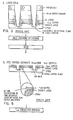
- Figs. 1-6 are schematic views illustrating various stages of a multilayer printed circuit board during a prior art process for producing it.
- Figs 7-9 are schematic views similar to Figs. 4-6 and including the neutralization process of the present invention.
- a prior art method or process for producing a multilayer printed circuit board will be briefly described.
- Fig. 1 there is shown a basic starting structure which comprises a 50pm copper carrier layer bonded to a chromium interface layer having a thickness in the order of 5...10 nm.
- the chromium layer is bonded to a 5 ⁇ m copper layer having a dendritic surface.
- the underside of the 5 ⁇ m copper layer is zinc surface treated to provide a thin zincate layer.
- the 50 ⁇ m copper carrier is a peel-apart-copper foil and it is known in the art as "Double Thin", a trade name of the Yates Corporation.
- the chromium interface layer is essential for peeling the copper carrier foil from the 5 ⁇ m copper layer.
- the 5 ⁇ m copper layer is the base structure of printed circuit lines and has a dendritic surface to enhance mechanical bonding during the lamination process along with a zinc treatment.
- the zincate layer promotes adhesion between copper and epoxy.
- This basic structure may be purchased from the Yates Corporation. As shown in Fig. 2, the basic structure is laminated by suitable heat and pressure to epoxy which contains one or more internal copper planes which serve as signal and ground planes.
- the laminate structure then goes through a blind via process wherein the surface is prepared by pumice scrubbing to provide a uniform copper surface for photoresist and in a dip operation, BTA (benzo triazole) is-applied to prevent corrosion.
- BTA benzo triazole
- the resist Riston a trade name of E.I. duPont de Nemours Co.
- This is followed by exposing with UV the hole pattern for the blind hole vias and then developing with methyl chloroform to provide the structure shown in Fig. 3.
- the developed structure is etched at ca. 54 0 C for approximately 3 minutes with a cupric chloride etchant which contains 1.0 normal HC1 acid to provide blind via holes down to the epoxy, as shown in Fig. 4.
- the blind via holes are laser drilled down to the internal copper planes in the epoxy, as shown in Fig. 5. It should be noted that by the time the laser drilling operation takes place, a portion of the zincate layer surrounding the via holes has been undercut or destroyed. This is more clearly shown in Fig. 6.
- the laser drilling operation is followed by hole cleaning operations and seeding.
- the hole cleaning operations involve vapor blasting with pumice followed by chemical dipping. In seeding, the holes are chemically treated to provide a suitable deposition surface for electroless copper plating.
- the 50 ⁇ m peel-apart-copper along with the chromium layer is peeled and separated from the 5 ⁇ m copper layer.
- the etching operation and the peel-apart operation there is a considerable lapse of time.
- free negative chloride ions are generated from the HC1 which attack or destroy the thin zincate layer between the 5 pm-copper and the epoxy.
- the zincate will start to weaken within 12 hours and the time between the etching operation and the peel-apart operation generally runs around 4 to 6 weeks.
- the primary function of the zincate layer is to promote adhesion between the copper and the epoxy.
- the zincate layer is sufficiently weakened or destroyed by the chloride ions, peeling off of the peel-apart-copper and chromium layer will result in the 5 ⁇ m copper layer being torn or separated from the epoxy, particularly in the areas surrounding the via holes.
- the 5 ⁇ m copper goes through the conventional circuitizing process wherein printed circuit lines are formed.
- satisfactory completion of the printed circuitry cannot be accomplished with the surface condition of the 5 ⁇ m copper shown in Fig. 6.
- Figs. 7-9 illustrate the application of the present invention to the prior art process just described.
- the etch process of Fig. 7 is the same as that described in connection with Fig. 4.
- the neutralization process of the present invention is carried out immediately following the completion of etching.
- the process makes use of Neutra Clean which comprises the following constituents:
- the alkyl aryl sulfonate is a wetting agent which allows for uniform wetting of the via hole without allowing the formation of bubbles.
- Ammonium sulfite and sodium sulfite are cleaning soaps. Ammonium chloride and sodium chloride attract the chloride ions from the cupric chloride etchant.
- the etched board is subjected to the following operations:
- the dip operations are used to create uniform wetting without the formation of bubbles so that the Neutra-Clean can effectively penetrate down into the the via hole and attract the chloride ions.
- the second dip operation provides a safety factor to insure that bubbles are not formed.
- the de-ionized water feed and rinse operations rinse out and remove the Neutra-Clean and any residuals due to chemical reaction.
Landscapes
- Engineering & Computer Science (AREA)
- Manufacturing & Machinery (AREA)
- Microelectronics & Electronic Packaging (AREA)
- Physics & Mathematics (AREA)
- Optics & Photonics (AREA)
- Manufacturing Of Printed Wiring (AREA)
- Production Of Multi-Layered Print Wiring Board (AREA)
Applications Claiming Priority (2)
| Application Number | Priority Date | Filing Date | Title |
|---|---|---|---|
| US392849 | 1982-06-28 | ||
| US06/392,849 US4398993A (en) | 1982-06-28 | 1982-06-28 | Neutralizing chloride ions in via holes in multilayer printed circuit boards |
Publications (2)
| Publication Number | Publication Date |
|---|---|
| EP0097835A1 true EP0097835A1 (de) | 1984-01-11 |
| EP0097835B1 EP0097835B1 (de) | 1986-04-16 |
Family
ID=23552262
Family Applications (1)
| Application Number | Title | Priority Date | Filing Date |
|---|---|---|---|
| EP83105440A Expired EP0097835B1 (de) | 1982-06-28 | 1983-06-01 | Verfahren zur Neutralisierung von Chlorid-Ionen in Verbindungslöchern bei gedruckten Mehrschichtschaltungen |
Country Status (4)
| Country | Link |
|---|---|
| US (1) | US4398993A (de) |
| EP (1) | EP0097835B1 (de) |
| JP (1) | JPS596597A (de) |
| DE (1) | DE3363036D1 (de) |
Cited By (1)
| Publication number | Priority date | Publication date | Assignee | Title |
|---|---|---|---|---|
| CN107770964A (zh) * | 2017-10-18 | 2018-03-06 | 开平依利安达电子第三有限公司 | 一种线路板穿孔工艺 |
Families Citing this family (17)
| Publication number | Priority date | Publication date | Assignee | Title |
|---|---|---|---|---|
| US4622095A (en) * | 1985-10-18 | 1986-11-11 | Ibm Corporation | Laser stimulated halogen gas etching of metal substrates |
| KR900003157B1 (ko) * | 1986-04-02 | 1990-05-09 | 가부시끼가이샤 히다찌세이샤꾸쇼 | 스루호울 도금의 전처리 방법 |
| US4687539A (en) * | 1986-10-29 | 1987-08-18 | International Business Machines Corp. | End point detection and control of laser induced dry chemical etching |
| US4991285A (en) * | 1989-11-17 | 1991-02-12 | Rockwell International Corporation | Method of fabricating multi-layer board |
| GB9015820D0 (en) * | 1990-07-18 | 1990-09-05 | Raychem Ltd | Processing microchips |
| US5158645A (en) * | 1991-09-03 | 1992-10-27 | International Business Machines, Inc. | Method of external circuitization of a circuit panel |
| GB9420182D0 (en) * | 1994-10-06 | 1994-11-23 | Int Computers Ltd | Printed circuit manufacture |
| EP0744884A3 (de) * | 1995-05-23 | 1997-09-24 | Hitachi Chemical Co Ltd | Verfahren zur Herstellung einer mehrschichtigen Leiterplatte |
| JP3612594B2 (ja) | 1998-05-29 | 2005-01-19 | 三井金属鉱業株式会社 | 樹脂付複合箔およびその製造方法並びに該複合箔を用いた多層銅張り積層板および多層プリント配線板の製造方法 |
| KR100760432B1 (ko) * | 1999-03-23 | 2007-09-20 | 서키트 호일 룩셈부르크 트레이딩 에스.에이 알. 엘. | 다층 인쇄회로기판의 제작방법 및 이에 이용되는 복합 호일 |
| LU90376B1 (en) * | 1999-03-23 | 2000-09-25 | Circuit Foil Luxembourg Trading Sarl | Method for manufacturing a multilayer printed circuit board and composite foil for use therein |
| US6207350B1 (en) * | 2000-01-18 | 2001-03-27 | Headway Technologies, Inc. | Corrosion inhibitor for NiCu for high performance writers |
| US6447929B1 (en) * | 2000-08-29 | 2002-09-10 | Gould Electronics Inc. | Thin copper on usable carrier and method of forming same |
| US20060108336A1 (en) * | 2004-11-23 | 2006-05-25 | Northrop Grumman Corporation | Fabrication process for large-scale panel devices |
| CN108971539B (zh) * | 2018-06-15 | 2020-07-24 | 深圳崇达多层线路板有限公司 | 一种防止微钻断针的钻孔方法 |
| CN108848622A (zh) * | 2018-08-15 | 2018-11-20 | 四川普瑞森电子有限公司 | 一种环保节水的除胶渣化学沉铜线的方法 |
| CN110225675A (zh) * | 2019-03-21 | 2019-09-10 | 深圳崇达多层线路板有限公司 | 一种薄芯板线路板的制作方法 |
Family Cites Families (1)
| Publication number | Priority date | Publication date | Assignee | Title |
|---|---|---|---|---|
| US4155775A (en) * | 1977-12-12 | 1979-05-22 | International Business Machines Corporation | Cleaning of high aspect ratio through holes in multilayer printed circuit boards |
-
1982
- 1982-06-28 US US06/392,849 patent/US4398993A/en not_active Expired - Lifetime
-
1983
- 1983-04-18 JP JP58067178A patent/JPS596597A/ja active Granted
- 1983-06-01 DE DE8383105440T patent/DE3363036D1/de not_active Expired
- 1983-06-01 EP EP83105440A patent/EP0097835B1/de not_active Expired
Non-Patent Citations (2)
| Title |
|---|
| "Soviet Inventions Illustrated" Week D 28, 19 August 1981 Sections L03, E37, V04 & SU-A-773976 * The text * * |
| WESCON CONFERENCE RECORD, vol. 25, September 1981, El Segundo P.J. BUD et al. "Aqueous cleaning for high reliability", pages 1-14 * Page 2, left-hand column, line 49 - page 3, left-hand column, line 4; page 10, right-hand column, * |
Cited By (1)
| Publication number | Priority date | Publication date | Assignee | Title |
|---|---|---|---|---|
| CN107770964A (zh) * | 2017-10-18 | 2018-03-06 | 开平依利安达电子第三有限公司 | 一种线路板穿孔工艺 |
Also Published As
| Publication number | Publication date |
|---|---|
| JPH0114720B2 (de) | 1989-03-14 |
| DE3363036D1 (en) | 1986-05-22 |
| US4398993A (en) | 1983-08-16 |
| EP0097835B1 (de) | 1986-04-16 |
| JPS596597A (ja) | 1984-01-13 |
Similar Documents
| Publication | Publication Date | Title |
|---|---|---|
| EP0097835B1 (de) | Verfahren zur Neutralisierung von Chlorid-Ionen in Verbindungslöchern bei gedruckten Mehrschichtschaltungen | |
| US4705592A (en) | Process for producing printed circuits | |
| US5707893A (en) | Method of making a circuitized substrate using two different metallization processes | |
| EP0591887A2 (de) | Gedruckte Leiterplatte | |
| JPH0783168B2 (ja) | プリント板の製造方法 | |
| KR100749444B1 (ko) | 에칭된 회로의 제조방법 | |
| WO1998009485A1 (en) | Pattern plating method for fabricating printed circuit boards | |
| EP0472158A2 (de) | Verfahren zur Herstellung einer gedruckten Leiterplatte | |
| EP0476065B1 (de) | Verfahren zur erhöhung des isolationswiderstandes von leiterplatten | |
| JP3750140B2 (ja) | 配線板の製造法 | |
| US5653893A (en) | Method of forming through-holes in printed wiring board substrates | |
| JP5298740B2 (ja) | 多層回路基板の製造方法 | |
| CN115843155A (zh) | Pcb制作方法 | |
| JP2003115662A (ja) | 半導体装置用基板の製造方法 | |
| JPH08148810A (ja) | プリント配線板の製造法 | |
| US5221418A (en) | Method for improving the surface insulation resistance of printed circuits | |
| JP2531466B2 (ja) | 印刷配線板の製造方法 | |
| JP2003031953A (ja) | ビルドアップ基板の製造方法 | |
| JPH03201592A (ja) | プリント配線板の製造法 | |
| JPH08139435A (ja) | プリント配線板の製造方法 | |
| JP3763666B2 (ja) | プリント配線板の製造方法 | |
| JP2595917B2 (ja) | 印刷配線板の製造方法 | |
| JPH104272A (ja) | 多層プリント配線板の製造方法 | |
| JPS59175797A (ja) | 多層プリント板の製造方法 | |
| JPH1070353A (ja) | 銅被覆ポリイミド基板を用いた電子回路基板の製造方法 |
Legal Events
| Date | Code | Title | Description |
|---|---|---|---|
| PUAI | Public reference made under article 153(3) epc to a published international application that has entered the european phase |
Free format text: ORIGINAL CODE: 0009012 |
|
| AK | Designated contracting states |
Designated state(s): DE FR GB |
|
| 17P | Request for examination filed |
Effective date: 19840426 |
|
| GRAA | (expected) grant |
Free format text: ORIGINAL CODE: 0009210 |
|
| AK | Designated contracting states |
Kind code of ref document: B1 Designated state(s): DE FR GB |
|
| REF | Corresponds to: |
Ref document number: 3363036 Country of ref document: DE Date of ref document: 19860522 |
|
| ET | Fr: translation filed | ||
| PLBE | No opposition filed within time limit |
Free format text: ORIGINAL CODE: 0009261 |
|
| STAA | Information on the status of an ep patent application or granted ep patent |
Free format text: STATUS: NO OPPOSITION FILED WITHIN TIME LIMIT |
|
| 26N | No opposition filed | ||
| PGFP | Annual fee paid to national office [announced via postgrant information from national office to epo] |
Ref country code: FR Payment date: 19950606 Year of fee payment: 13 |
|
| PGFP | Annual fee paid to national office [announced via postgrant information from national office to epo] |
Ref country code: DE Payment date: 19950616 Year of fee payment: 13 |
|
| PGFP | Annual fee paid to national office [announced via postgrant information from national office to epo] |
Ref country code: GB Payment date: 19960520 Year of fee payment: 14 |
|
| PG25 | Lapsed in a contracting state [announced via postgrant information from national office to epo] |
Ref country code: FR Effective date: 19970228 |
|
| PG25 | Lapsed in a contracting state [announced via postgrant information from national office to epo] |
Ref country code: DE Effective date: 19970301 |
|
| REG | Reference to a national code |
Ref country code: FR Ref legal event code: ST |
|
| PG25 | Lapsed in a contracting state [announced via postgrant information from national office to epo] |
Ref country code: GB Effective date: 19970601 |
|
| GBPC | Gb: european patent ceased through non-payment of renewal fee |
Effective date: 19970601 |