EP0098074A1 - Emittergekoppelte Logikschaltung - Google Patents
Emittergekoppelte Logikschaltung Download PDFInfo
- Publication number
- EP0098074A1 EP0098074A1 EP83303428A EP83303428A EP0098074A1 EP 0098074 A1 EP0098074 A1 EP 0098074A1 EP 83303428 A EP83303428 A EP 83303428A EP 83303428 A EP83303428 A EP 83303428A EP 0098074 A1 EP0098074 A1 EP 0098074A1
- Authority
- EP
- European Patent Office
- Prior art keywords
- input signal
- logic
- level
- emitter coupled
- logic circuit
- Prior art date
- Legal status (The legal status is an assumption and is not a legal conclusion. Google has not performed a legal analysis and makes no representation as to the accuracy of the status listed.)
- Granted
Links
Images
Classifications
-
- H—ELECTRICITY
- H03—ELECTRONIC CIRCUITRY
- H03K—PULSE TECHNIQUE
- H03K19/00—Logic circuits, i.e. having at least two inputs acting on one output; Inverting circuits
- H03K19/02—Logic circuits, i.e. having at least two inputs acting on one output; Inverting circuits using specified components
- H03K19/08—Logic circuits, i.e. having at least two inputs acting on one output; Inverting circuits using specified components using semiconductor devices
- H03K19/082—Logic circuits, i.e. having at least two inputs acting on one output; Inverting circuits using specified components using semiconductor devices using bipolar transistors
- H03K19/086—Emitter coupled logic
Definitions
- the present invention relates to an emitter coupled logic (ECL) circuit, more particularly to an ECL circuit receiving two complementary input logic signals and controlled by a set input signal.
- ECL emitter coupled logic
- an ECL circuit is comprised of a differential amplifier. Therefore, it is possible to achieve very high speed operation.
- a recent trend has been for the application of an ECL circuit to a logic gate.
- the ECL circuit is provided with a set circuit. If the ECL circuit operates as a gate for passage of a certain logic input signal therethrough, the set circuit functions to selectively control that passage. For example, if the set input signal (C) has logic "L” (low), the set circuit will allow the logic input signal (A) to pass the ECL circuit, while if the set input signal (C) has logic "H” (high), the set circuit will not allow the logic input signal (A) to pass through the ECL circuit.
- one side of the differential amplifier comprising the ECL circuit receives the logic input signal, while the other side receives a reference voltage signal (V ref ) ⁇
- V ref reference voltage signal
- Use of such complementary logic input signals (A, A) enlarges the difference between two control input signals to (A - A) and, accordingly, offers the advantages of increased noise margin and further high speed operation.
- the amplifier can be driven by a control input signal having a magnitude of, for example, 400 mV.
- An emitter-coupled logic circuit comprises a differential transistor pair to which logic input signals are complementarily applied as control input signals thereof, the differential transistor pair having emitters coupled to each other; and a set transistor to which a set input signal is applied as a control input signal thereof, the set transistor being connected to one transistor of the differential transistor pair in parallel,and is characterized in that the high potential logic level of the set input signal is higher than the high potential logic level of the logic input signal by a first predetermined level difference; and the low potential logic level of the set input signal is lower than the low potential logic level of the logic input signal by a second predetermined level difference.
- the magnitude difference between the high and low logic levels of the logic input signal is set smaller than the magnitude difference between the high and low logic levels of the set input signal.
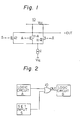
- FIG. 1 is a circuit diagram of an ECL circuit to which the present invention is adapted.
- reference characters 11-A and 11-A indicate an emitter coupled pair of differential transistors (differential amplifier). Each collector thereof is connected, via a resistor, to a power source V CC . Each emitter thereof is connected, via a common constant current source I, to a ground V EE .
- the complementary logic input signals A and A are applied, as control input signals, to the differential transistor pair 11-A and 11-A.
- V ref reference voltage signal
- the ECL circuit produces an output OUT of logic "L” or “H” in accordance with the logic "H” or "L” of signal A.
- a transistor 12 represents the set circuit, which transistor 12 is also emitter coupled with the differential transistor pair ll-A and 11-A.
- the set transistor 12 receives, as a control input signal, a set input signal S.
- the set input signal S is set at the logic "H”
- the collector of the set transistor 12 is forcibly clamped at the logic "L”
- the output OUT is maintained at the logic "L”.
- logic changes by the logic input signal A do not influence logic changes of the output OUT. Consequently, the ECL circuit 10 then operates as a closed gate.
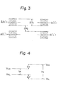
- FIG. 2 is a block diagram schematically and briefly showing a circuit mode in which the ECL circuit of Fig. 1 is introduced.
- the ECL circuit 10 of Fig. 1 is illustrated in the form of an OR gate, via which OR gate, a logic circuit A and a logic circuit B are connected with each other. Whether the logic input signal from the logic circuit A is to be transferred to the logic circuit B is determined by the set input signal from the set input circuit S . When the set input signal S is logic "H”, the logic input signal from the logic circuit A is not transferred to the logic circuit B, while, when the set input signal is logic "L”, the logic input signal is transferred to the logic circuit B.
- ECL circuit 10 When the set input signal S is used to set the ECL circuit 10 (ECL circuit 10 operates as closed gate) or to reset it (ECL circuit 10 operates as open gate), there is often a problem in that the ECL circuit 10 may fail to be set when it is supposed to be set or may be inadvertently set when it is not.
- V ref the reference voltage signal (V ref ) is used as the logic input signal A for the transistor 11-A' of Fig. 1, there is no problem since the reference voltage (V ref ) level itself is constant. Thus, the range of relative variance between the reference voltage signal level and the other signal levels is relatively small. If such reference voltage signal (V ref ) is used, however the advantages of an increased noise margin and high speed operation cannot be expected.
- V ref the reference voltage signal
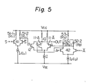
- Figure 3 is a level diagram for explaining the problem in more detail.
- the chain-dotted lines represent design values (desired values) of logic "H” and “L” levels for each of the logic input signals A and A and the set input signal S.
- the hatched areas associated with the chain-dotted lines denote ranges of variance in levels.
- the problem was overcome by externally supplying a set signal S to ensure that logic "H” had a fully high level and logic "L” had a fully low level.
- Use of such an externally supplied set signal is clearly inconvenient. Accordingly, strong demand has existed to deal with the problem inside the ECL circuit without employing such a signal.
- a certain relationship in level between the logic input signals and the set input signal is created so as to prevent this problem even with such level variance.
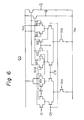
- Figure 4 is a level diagram used for explaining how to the logic levels in the ECL circuit according to the present invention.
- a magnitude V A between a level corresponding to the logic "H” of the logic input signal A (same applies to signal A) and a level corresponding to the logic "L” thereof is preset to be smaller than an identical magnitude V S for the set input signal S.
- a design value (desired value) V AH of the level corresponding to the logic “H” of the logic input signal is set lower by ⁇ v than a design value (desired value) V SH of the level corresponding to the logic "H” of the set input signal, while a design value (desired value) V AL of the level corresponding to the logic “L” of the logic input signal is set higher by ⁇ v' than a design value (desired value) V SL of the level corresponding to the logic "L” of the set input signal.
- the object of the present invention is attained by setting the logic level of the high voltage side of the set input signal higher than the logic level of the high voltage side of the logic input signal by a predetermined level difference and by setting the logic level of the low voltage side of the set input signal lower than the logic level of the low voltage side of the logic input signal by a predetermined level difference. Therefore, the magnitude difference between the high and low logic levels of the logic input signal is set smaller than the magnitude difference between the high and low logic levels of the set input signal.
- the magnitude V S is set to be 450 mV
- the range of level in which the logic input signal level can exist is preset to be smaller than the range of level in which the set input signal level can exist. This makes it possible to avoid use of an externally supplied level for determining the level of the set input signal S.
- This method of setting the levels of the signals can be realized without any particular complicated structure in the ECL circuit.
- FIG. 5 is a detailed circuit diagram of an ECL circuit according to the present invention.
- members referenced by numerals and symbols 10, 11-A, 11- A , 12, I, and OUT have been explained previously.
- the difference here is that the logic input signals A and A are level converted into logic input signals a and a.
- the set input signal S is level converted into a set input signal s.
- These level conversions are performed by a first ECL circuit element 41 and a second ECL circuit element 42 for the set input signal S and the logic input signals A and A, respectively.
- the first ECL circuit element 41 includes a pair of first resistors 51-1 and 51-2, each having a resistance value of R 1 .
- the second ECL element circuit 42 includes a pair of second resistors 52-1 and 52-2, each having a resistance value of R 2 , and a third resistor 53 having a resistance value of R 3'
- the first ECL circuit element 41 is directly connected to the voltage source V CC , while the second ECL circuit element 42 is connected via the third resistor 53.
- a current value i 2 in a constant current source I2 connected to the second ECL circuit element 42, is suitably determined. Based on this value i 2 , the resistance value R 3 of the third resistor 53 is determined. This determination is effected, with reference to Fig. 4, along with equation (1).
- ⁇ v is, according to the previously mentioned example, 25 mV.
- ⁇ v' is, according to the previously mentioned example, 25 mV.
- Figure 6 is a circuit diagram of an application of the ECL circuit in Fig. 5.
- the flip flop circuit 60 receives data signal D and is synchronized by a clock signal CK.
- the circuit 60 produces a complementary output pair of Q and Q.
- Signals V CS indicate chip selection signals.
- reference characters 61-A, 61- A and 61'-A, 61'- A represent differential transistor pairs, each pair corresponding to the differential transistor pair 11-A, 11-A in Fig. 5.
- Reference numerals 62 and 62' represent set transistors, each corresponding to the set transistors 12 in Fig. 5, controlled by set input signal S.
- the transistor pair 42 of Fig. 5 corresponds to a transistor pair 63 in Fig. 6. No transistor pair corresponding to the transistor pair 41 of Fig. 5 is illustrated in Fig. 6, however, the resultant output thereof is indicated by the same character s.
Landscapes
- Engineering & Computer Science (AREA)
- Power Engineering (AREA)
- Physics & Mathematics (AREA)
- Computer Hardware Design (AREA)
- Computing Systems (AREA)
- General Engineering & Computer Science (AREA)
- Mathematical Physics (AREA)
- Logic Circuits (AREA)
Applications Claiming Priority (2)
| Application Number | Priority Date | Filing Date | Title |
|---|---|---|---|
| JP110619/82 | 1982-06-29 | ||
| JP57110619A JPS592435A (ja) | 1982-06-29 | 1982-06-29 | Ecl回路 |
Publications (2)
| Publication Number | Publication Date |
|---|---|
| EP0098074A1 true EP0098074A1 (de) | 1984-01-11 |
| EP0098074B1 EP0098074B1 (de) | 1986-09-24 |
Family
ID=14540387
Family Applications (1)
| Application Number | Title | Priority Date | Filing Date |
|---|---|---|---|
| EP83303428A Expired EP0098074B1 (de) | 1982-06-29 | 1983-06-14 | Emittergekoppelte Logikschaltung |
Country Status (5)
| Country | Link |
|---|---|
| US (1) | US4551639A (de) |
| EP (1) | EP0098074B1 (de) |
| JP (1) | JPS592435A (de) |
| DE (1) | DE3366431D1 (de) |
| IE (1) | IE54541B1 (de) |
Families Citing this family (11)
| Publication number | Priority date | Publication date | Assignee | Title |
|---|---|---|---|---|
| JPS60144022A (ja) * | 1983-12-30 | 1985-07-30 | Hitachi Ltd | 差動形論理回路 |
| US4810908A (en) * | 1986-12-01 | 1989-03-07 | Hirokazu Suzuki | Semiconductor logic circuit comprising clock driver and clocked logic circuit |
| US4871931A (en) * | 1987-10-30 | 1989-10-03 | Gazelle Microcircuits, Inc. | Logic circuit resistant to errors due to supply fluctuations |
| US5001361A (en) * | 1988-05-13 | 1991-03-19 | Fujitsu Limited | Master-slave flip-flop circuit |
| EP0365732B1 (de) * | 1988-10-28 | 1993-08-18 | International Business Machines Corporation | Zweistufige Adressendekodierschaltung für Halbleiterspeicher |
| DE58906599D1 (de) * | 1989-09-11 | 1994-02-10 | Siemens Ag | Kippschaltung mit Schalthysterese. |
| US5079452A (en) * | 1990-06-29 | 1992-01-07 | Digital Equipment Corporation | High speed ECL latch with clock enable |
| DE69124176T2 (de) * | 1990-08-29 | 1997-07-10 | Motorola Inc | Logischer BICMOS Schaltkreis mit einem CML-Ausgang |
| US5258661A (en) * | 1992-04-20 | 1993-11-02 | International Business Machines Corporation | High noise tolerance receiver |
| US5751169A (en) * | 1996-05-02 | 1998-05-12 | Motorola, Inc. | Emitter coupled logic (ECL) gate which generates intermediate signals of four different voltages |
| US6847233B1 (en) | 2001-07-12 | 2005-01-25 | Mediatek Inc. | Emitter coupled logic circuit with a data reload function |
Citations (1)
| Publication number | Priority date | Publication date | Assignee | Title |
|---|---|---|---|---|
| US3321639A (en) * | 1962-12-03 | 1967-05-23 | Gen Electric | Direct coupled, current mode logic |
Family Cites Families (7)
| Publication number | Priority date | Publication date | Assignee | Title |
|---|---|---|---|---|
| DE1941264C3 (de) * | 1969-08-13 | 1975-07-17 | Siemens Ag, 1000 Berlin Und 8000 Muenchen | Asynchrone RS-Kippstufe in ECL-Technik |
| US3906212A (en) * | 1971-08-18 | 1975-09-16 | Siemens Ag | Series-coupled emitter coupled logic (ECL) circuit having a plurality of independently controllable current paths in a lower plane |
| JPS522161A (en) * | 1975-06-24 | 1977-01-08 | Hitachi Ltd | Logic circuit |
| GB1592246A (en) * | 1976-09-23 | 1981-07-01 | Isaac T P | Sound projection system |
| JPS54128656A (en) * | 1978-03-30 | 1979-10-05 | Nec Corp | Flip flop circuit of current selection type |
| US4347446A (en) * | 1979-12-10 | 1982-08-31 | Amdahl Corporation | Emitter coupled logic circuit with active pull-down |
| JPS56107641A (en) * | 1980-01-31 | 1981-08-26 | Nec Corp | Semiconductor circuit equipment |
-
1982
- 1982-06-29 JP JP57110619A patent/JPS592435A/ja active Pending
-
1983
- 1983-06-09 US US06/502,560 patent/US4551639A/en not_active Expired - Lifetime
- 1983-06-14 DE DE8383303428T patent/DE3366431D1/de not_active Expired
- 1983-06-14 EP EP83303428A patent/EP0098074B1/de not_active Expired
- 1983-06-29 IE IE1528/83A patent/IE54541B1/en not_active IP Right Cessation
Patent Citations (1)
| Publication number | Priority date | Publication date | Assignee | Title |
|---|---|---|---|---|
| US3321639A (en) * | 1962-12-03 | 1967-05-23 | Gen Electric | Direct coupled, current mode logic |
Also Published As
| Publication number | Publication date |
|---|---|
| IE831528L (en) | 1983-12-29 |
| IE54541B1 (en) | 1989-11-08 |
| DE3366431D1 (en) | 1986-10-30 |
| JPS592435A (ja) | 1984-01-09 |
| EP0098074B1 (de) | 1986-09-24 |
| US4551639A (en) | 1985-11-05 |
Similar Documents
| Publication | Publication Date | Title |
|---|---|---|
| US4833342A (en) | Reference potential generating circuit | |
| US4453095A (en) | ECL MOS Buffer circuits | |
| JP2525346B2 (ja) | 定電流源回路を有する差動増幅回路 | |
| EP0098074B1 (de) | Emittergekoppelte Logikschaltung | |
| EP0453185B1 (de) | ECL-Ausgangspufferschaltung | |
| US4677321A (en) | TTL compatible input buffer | |
| JPS62217714A (ja) | 高電圧検出回路 | |
| US4641081A (en) | Semiconductor circuit of MOS transistors for generation of reference voltage | |
| EP0193901A2 (de) | Komparatorschaltung mit verbesserten Ausgangseigenschaften | |
| US4359653A (en) | Integrated circuit having a plurality of current mode logic gates | |
| US4267501A (en) | NMOS Voltage reference generator | |
| US4045690A (en) | High speed differential to ttl converter | |
| US6411159B1 (en) | Circuit for controlling current levels in differential logic circuitry | |
| US5136183A (en) | Integrated comparator circuit | |
| US4368395A (en) | Differential linear to digital translator | |
| JPH118542A (ja) | 出力回路 | |
| US5306964A (en) | Reference generator circuit for BiCMOS ECL gate employing PMOS load devices | |
| US4967106A (en) | Emitter-coupled logic circuit | |
| US3934157A (en) | TTL circuit | |
| JP2002015599A (ja) | 半導体記憶装置 | |
| US5177380A (en) | ECL latch with single-ended and differential inputs | |
| JPH054855B2 (de) | ||
| US4980581A (en) | Differential ECL bus tri-state detection receiver | |
| US5331229A (en) | CMOS/ECL signal level converter | |
| US5376845A (en) | Apparatus and method for ECL-like signal to CMOS signal conversion |
Legal Events
| Date | Code | Title | Description |
|---|---|---|---|
| PUAI | Public reference made under article 153(3) epc to a published international application that has entered the european phase |
Free format text: ORIGINAL CODE: 0009012 |
|
| AK | Designated contracting states |
Designated state(s): DE FR GB |
|
| 17P | Request for examination filed |
Effective date: 19840615 |
|
| GRAA | (expected) grant |
Free format text: ORIGINAL CODE: 0009210 |
|
| AK | Designated contracting states |
Kind code of ref document: B1 Designated state(s): DE FR GB |
|
| REF | Corresponds to: |
Ref document number: 3366431 Country of ref document: DE Date of ref document: 19861030 |
|
| ET | Fr: translation filed | ||
| PLBE | No opposition filed within time limit |
Free format text: ORIGINAL CODE: 0009261 |
|
| STAA | Information on the status of an ep patent application or granted ep patent |
Free format text: STATUS: NO OPPOSITION FILED WITHIN TIME LIMIT |
|
| 26N | No opposition filed | ||
| PGFP | Annual fee paid to national office [announced via postgrant information from national office to epo] |
Ref country code: FR Payment date: 20000612 Year of fee payment: 18 |
|
| PGFP | Annual fee paid to national office [announced via postgrant information from national office to epo] |
Ref country code: GB Payment date: 20000614 Year of fee payment: 18 Ref country code: DE Payment date: 20000614 Year of fee payment: 18 |
|
| PG25 | Lapsed in a contracting state [announced via postgrant information from national office to epo] |
Ref country code: GB Free format text: LAPSE BECAUSE OF NON-PAYMENT OF DUE FEES Effective date: 20010614 |
|
| GBPC | Gb: european patent ceased through non-payment of renewal fee |
Effective date: 20010614 |
|
| PG25 | Lapsed in a contracting state [announced via postgrant information from national office to epo] |
Ref country code: FR Free format text: LAPSE BECAUSE OF NON-PAYMENT OF DUE FEES Effective date: 20020228 |
|
| PG25 | Lapsed in a contracting state [announced via postgrant information from national office to epo] |
Ref country code: DE Free format text: LAPSE BECAUSE OF NON-PAYMENT OF DUE FEES Effective date: 20020403 |