EP0365732B1 - Zweistufige Adressendekodierschaltung für Halbleiterspeicher - Google Patents
Zweistufige Adressendekodierschaltung für Halbleiterspeicher Download PDFInfo
- Publication number
- EP0365732B1 EP0365732B1 EP88480068A EP88480068A EP0365732B1 EP 0365732 B1 EP0365732 B1 EP 0365732B1 EP 88480068 A EP88480068 A EP 88480068A EP 88480068 A EP88480068 A EP 88480068A EP 0365732 B1 EP0365732 B1 EP 0365732B1
- Authority
- EP
- European Patent Office
- Prior art keywords
- decoder
- stage
- circuit
- transistors
- signals
- Prior art date
- Legal status (The legal status is an assumption and is not a legal conclusion. Google has not performed a legal analysis and makes no representation as to the accuracy of the status listed.)
- Expired - Lifetime
Links
- 230000015654 memory Effects 0.000 title description 16
- 239000004065 semiconductor Substances 0.000 title description 6
- 230000001960 triggered effect Effects 0.000 claims description 2
- 230000000295 complement effect Effects 0.000 description 12
- 238000005516 engineering process Methods 0.000 description 8
- 230000008901 benefit Effects 0.000 description 4
- 238000010276 construction Methods 0.000 description 3
- 238000010586 diagram Methods 0.000 description 3
- 238000003491 array Methods 0.000 description 2
- 230000015556 catabolic process Effects 0.000 description 2
- 238000006731 degradation reaction Methods 0.000 description 2
- 230000000630 rising effect Effects 0.000 description 2
- 230000003068 static effect Effects 0.000 description 2
- 230000001154 acute effect Effects 0.000 description 1
- 230000003321 amplification Effects 0.000 description 1
- 238000006243 chemical reaction Methods 0.000 description 1
- 230000001143 conditioned effect Effects 0.000 description 1
- 230000003111 delayed effect Effects 0.000 description 1
- 230000001419 dependent effect Effects 0.000 description 1
- 230000006870 function Effects 0.000 description 1
- 230000036039 immunity Effects 0.000 description 1
- 238000003199 nucleic acid amplification method Methods 0.000 description 1
- 230000008520 organization Effects 0.000 description 1
- 230000004044 response Effects 0.000 description 1
- 239000007787 solid Substances 0.000 description 1
- 230000000153 supplemental effect Effects 0.000 description 1
- 230000007704 transition Effects 0.000 description 1
Images

Classifications
-
- G—PHYSICS
- G11—INFORMATION STORAGE
- G11C—STATIC STORES
- G11C11/00—Digital stores characterised by the use of particular electric or magnetic storage elements; Storage elements therefor
- G11C11/21—Digital stores characterised by the use of particular electric or magnetic storage elements; Storage elements therefor using electric elements
- G11C11/34—Digital stores characterised by the use of particular electric or magnetic storage elements; Storage elements therefor using electric elements using semiconductor devices
- G11C11/40—Digital stores characterised by the use of particular electric or magnetic storage elements; Storage elements therefor using electric elements using semiconductor devices using transistors
- G11C11/41—Digital stores characterised by the use of particular electric or magnetic storage elements; Storage elements therefor using electric elements using semiconductor devices using transistors forming static cells with positive feedback, i.e. cells not needing refreshing or charge regeneration, e.g. bistable multivibrator or Schmitt trigger
- G11C11/413—Auxiliary circuits, e.g. for addressing, decoding, driving, writing, sensing, timing or power reduction
- G11C11/414—Auxiliary circuits, e.g. for addressing, decoding, driving, writing, sensing, timing or power reduction for memory cells of the bipolar type
- G11C11/415—Address circuits
-
- G—PHYSICS
- G11—INFORMATION STORAGE
- G11C—STATIC STORES
- G11C8/00—Arrangements for selecting an address in a digital store
- G11C8/10—Decoders
Definitions
- the present invention relates to semiconductor integrated circuits and more particularly to a two stage address decoder circuit for high speed large capacity Static Random Access Memories (SRAMs).
- SRAMs Static Random Access Memories
- a word address decoder circuit which generates select/unselect signals for appropriately selecting a plurality of memory cells in the same row of a memory cell array (in other words, those cells which are connected to the same word line), while the remaining cells remain unselected.
- the address decoder circuit receives word address signals, in true and complement form, of e.g. n bits, and generate one select signal among 2 n combinations of the address signals.
- CMOS or BICMOS driver to drive the heavy capacitive loads on the word lines of the memory array, typically comprised of CMOS 6-device SRAM cells.
- CML Current Mode Logic
- DCCS Differential Cascode Current Switch
- ECL Emitter Coupled Logic
- the decoder circuit may be understood as being composed of three circuit stages connected in cascade: a predecoding circuit of the ECL collector dotting type (CD), a level shifting circuit of the standard emitter follower type (EF), and a main decoding circuit so called a series gate circuit (SG) in CML technology.
- CD ECL collector dotting type
- EF level shifting circuit of the standard emitter follower type
- SG series gate circuit
- the CD circuit is used as the first layer of decoding. According to an original feature of the CD circuit, it is not necessary to generate explicitly the true and complement address signals, because the address receiver is included in the pre-decoder. However, this is not a definite advantage. True and complement address signals are generally available in a current switch environment. Alternatively, it is also possible to replace the complement address signals by a fixed reference voltage if supply and signal voltages are adequate. For each address signal, a receiver of the current switch type generates current information corresponding to the true and complement values. In others words, instead of using a voltage, a current provides the pre-decoding information. The collectors are all dotted together and a decoded address will correspond to no current flow in any of them.
- the purpose of the EF circuit is to generate predecoded signals with a number of Vbe DC shifts (depending on the number of diodes) in order to drive the SG circuit that follows. In others words, it operates as a level converter. This construction has some inconveniences, because it does not provide an efficient solution in optimizing said SG circuit.
- the third decoding layer consists of the SG circuit. Because, the signals that drive the SG circuit have already been predecoded by the CD circuit, a differential tree, where more than 2 transistors are connected in each branch, can be used. If this construction reduces the number of layers in the tree, it has a significant drawback in that the common emitter nodes are more heavily loaded, which in turn, results in slowing down the current switching. In addition, it is clear that the up level depends of Vcc (minus a number of Vbe's), while the down level is referenced to ground. Finally, the saturation control of the SG circuit is poor, and becomes even more acute when the supply voltages are reduced.
- VCC 0V
- VEE -5,2V
- the disclosed three stage address decoder is power consuming in that there is no means provided to cut down the DC power in any stage of the decoder, causing a continuous consumption of power in the quiescent state, even if the circuits are not selected.
- it has a limited flexibility and adaptability to different memory sizes and organizations because of the close interrelationships existing between the three circuits which in turn, makes it difficult to increase the number of the tree levels if so desired.
- a two stage address decoder circuit as defined in claim 1 for decoding n input address signals and n inverted address signals into 2 n decoded output signals.
- the decoder circuit includes: a first stage comprised of at least two predecoder circuits operable to develop predecoded output signals in response to input address signals and the corresponding inverted address signals.
- Each predecoder circuit consists of a low power high speed Differential Cascode Current Switch (DCCS) tree with its associated current source.
- the address decoder circuit further includes a second or final decoding stage comprised of 2 n final decoder (FD) circuits.
- Each FD circuit consists of a 2-way OR gate dynamically activated through a switched current source.
- the inputs of the 2-way OR gate are connected to one couple of said predecoded output signals.
- Final decoder circuits supply final decoded output signals to drive the word lines of a memory cell array.
- the switched current source is triggered by a control signal supplied by a clock generator so that the FD circuits consume power only when the control signal is active.
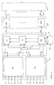
- Fig. 1 is a block diagram showing the general architecture of the address decode scheme to provide 1/64 decode signal to a SRAM, according to the teachings of the present invention.
- the two stage address decoder circuit AD is comprised of two main functional blocks.
- a predecoder block referenced PD comprising two predecoder circuits PDP and PDQ, is designed to operate as the first stage/section.
- Input address signals A1 to A3 (and inverted signals) are applied to the address lines of the predecoder PDP.
- Predecoded output signals P1 to P8 are available at the outputs of the PDP circuit. Similar construction applies to predecoder circuit PDQ respectively with input address signals A4 to A6 and predecoded output signals Q1 to Q8.
- Predecoder circuits PDQ and PDQ are identical and decode one out of 3 true/complement input address signals. As known, a three bit address signal can be decoded to provide eight different output signals.
- Two stage decoder circuit AD also includes a final decoder block FD to operate as the second stage and comprises 64 final decoder circuits referenced FD1 to FD64. They are adequately driven by the combinatorial set of predecoded output signals generated through the predecoding stages. For example, predecoded output signals P1 and Q1 are applied to FD1, while predecoded output signals P8 and Q8 are applied to FD64.
- each FD circuit is connected to a word line driver which is designed differently depending on wether the SRAM technology is pure bipolar or BICMOS.
- Each of the final decoder e.g. FD1 supplies a decoded output signal, e.g. X1, to a word line driver circuit, e.g. WLD1. All the 64 word line drivers WLD1 to WLD64 form word line driver block WLD.
- Word line drivers, e.g. WLD1 provide word line output signals, e.g. W1 on the word lines, e.g. WL1. The latter are connected in a standard way to the memory cells (not represented) of a memory cell array MA.
- a single circuit AD including several predecoder circuits and different word line driver blocks may service a plurality (K) of memory arrays (so called subarrays).
- the predecoders are built with a DCCS tree associated with an improved current source, and the final decoder circuits are each constituted of an OR gate loaded by a switched current source.
- final decoder circuits FD1 to FD64 operate under the control of a clock generator CG which provides control signals from a clock signal CLK.
- CG clock generator
- This CG circuit is recommended for optimized operation of address decoder AD to save power consumption.
- this generator delivers a Set Word Line (SWL) control signal, when the main clock signal CLK is activated.
- SWL Set Word Line
- Fig. 2 shows in details a typical ⁇ embodiment of one predecoder circuit, e.g. PDP and one final decoder circuit, e.g. FD1 of the address decoder AD of the present invention.
- predecoder circuit PDP is used for decoding three binary valued input signals A1 to A3 to one of eight binary valued output signals P1 to P8.
- the predecoder circuit PDP comprises one logical DCCS tree referenced STP, and one current source referenced CSP connected to the tree.
- the tree consists of a plurality of cells where each cell comprises a pair of transistors.
- the cells are arranged in levels corresponding to the number of address signals, and where each level is associated with a different one of the address signals.
- Level 1 comprising one cell (Q1, Q2), is associated with address signal A3.
- Level 2 is associated with address signal A2 and includes two cells (Q3, Q4, Q5, Q6).
- Level 3 is associated with address signal A1 and comprises four cells (Q7, Q8; Q9, Q10; Q11, Q12; Q13, Q14). Collectors of output transistors at level 3 are loaded by respective resistors R7, ..., R14 connected to a first supply voltage VH and of the same value.
- the address signals supplied to each cell are differential (true/complement) input address signals.
- Each cell comprises a pair of switching elements shown as transistors, whose emitters are coupled together and whose collectors provide output signals of the cell which are connected to the following level as input signals.
- the differential address signals are applied to the bases of the transistors of the cells. Each transistor functions as a switch to establish a current path from a current source in level 1 or a cell to another cell in the next level.
- the tree structure therefore, has the capability of establishing one of eight unique current paths depending upon the binary value of the address signals say bits: A1, A2 and A3. Each unique current path corresponds to one of the eight possible permutations which can be established for three binary valued input signals.
- an output transistor is turned on and then the corresponding predecoded output signal is at a down level, then the 7 others output transistors are cut off and the corresponding predecoded output signals is at VH.
- the current source CSP is simply formed by a single transistor connected between the common emitter of Q1 and Q2 and a second supply voltage GND while its base is connected to a reference voltage VREF.
- the usual single transistor is split into four elementary transistors T1.1 to T1.4 the base electrodes of which are tied together and connected to a reference voltage VREF supplied by a special antisaturation circuit operating in a current mirror mode.
- This unique antisaturation circuit includes transistor T0 mounted in a diode configuration since its base-collector junction is shorted, and loaded by resistor R0 connected to VH.
- Another load resistor RD in series with a diode D are connected in parallel with resistor R0.
- the STP tree shown in Fig. 2 is basically a 3 level DCCS circuit for pre-decoding the 3 address signals applied to the address lines.
- these complement (or inverted) address signals can be generated through a standard differential amplifier (not shown), comprised of two bipolar transistors having an emitter coupled configuration. The collectors of these transistors are connected through load resistors to a supply voltage Vref(m). The address signal is applied to the base electrode of one transistor, while the other base electrode is connected to a reference voltage Vref.
- each of the other reference voltages Vref(2), Vref(1) is successively determined with such a constant voltage increment.
- the latter must be as low as possible, to maximize the swing capability, but not too small to cause saturation of transistors, which in turn, could result in consequent speed degradation and failure in operation.
- the incremental voltage value between the different address signals in the DCCS tree has been chosen to be around 300 mv.
- the 300 mV of voltage incremental between the Vref(m) allows an automatic clamp of about 0.5 V across the collector-base junction of any transistor in the tree, which keeps all transistors far away from saturation.
- the level number m which also corresponds to the number of address signals to be decoded, such that m ⁇ 5.
- High value resistors R (in the range of 10 k ⁇ ) are provided at all the intermediate common emitter nodes in the DCCS tree to prevent these nodes to be charged to high value voltage through different leakage paths. Otherwise, this would lead to performance unpredictability, especially during the long periods of time the SRAM is not addressed.
- the design of the current source can be made differently depending on the type of cell that is used in the memory cell array. If the technology considered is a BICMOS one, the mirrored current in the transistor T0 is such that the predecoded output signals on the 8 collectors of the output transistors at the end of the DCCS tree will be driven with respect to GND at the down level. The respective high voltage on said signals will always follow VH.
- the goal of current source CSP is to drive the collectors of the output transistors (Q7 to Q14) as low as possible in order to be able to drive a BICMOS driver in the best conditions. It is well known that a BICMOS or a CMOS driver needs a large voltage swing to operate efficiently (overdrive Vgs above the threshold voltage).
- P1 VH-k′RD [( VH - Vbe ( Q 7))/ kRD + ( VH - Vbe ( Q 7) - Vbe ( Q 8))/ RD ]
- RD can be seen as a normalized value which determines the speed of the predecoder circuit. As a result, it is very easy to increase or to slow down the speed of the DCCS tree, since its performance is now mainly dependant on the value of RD.
- any FD circuit e.g. FD1 is basically a switchable OR gate built with emitter dot followers.
- the OR gate includes transistors T and T′ connected in parallel between VH and a common emitter or OUT node at the same potential as the OUT terminal. Said OUT node is connected to a switchable current source comprising transistor T1 and resistor R1 connected to GND.
- Signal SWL is applied at the base of transistor T1.
- a single control signal SWL may be sufficient to activate the FD circuits, for example, if they are of the self power-off type.
- a second control signal RWL Reset Word Line
- Control signal RWL is also generated by the CG circuit.
- a third transistor T2 is mounted in parallel with transistors T and T′, its base being driven by said control signal RWL.
- an additional transistor T ⁇ (not shown) may be added in parallel with transistors T and T′ in the OR gate, if a supplemental predecoder/current source PDR/CSR (not shown) is desired to increase the number of decoded output signal/lines. Therefore, SWL and RWL control signals are respectively used, to set a decoded word line within the cell array during a predetermined time window, and to turn off the 64 FD circuits. The word line that is selected corresponds to the set of collector outputs that are low. The address is kept stable during the READ operation, the end of which is conditioned by the RWL control signal. This will become even more apparent with the description of Fig. 3.
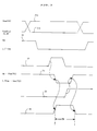
- Fig. 3 shows typical waveforms in the data path of the two stage address decoder circuit of the present invention.
- Curves 31a and 31b show the address input signals An and An ⁇ and illustrate the voltage difference of 0.3 V used to distinguish the true/complement signals.
- Curve 32 shows one typical predecoded output signal P1 to P8 or Q1 to Q8.
- Curve 33 is the SWL control signal. It is a calibrated pulse related to the total memory cycle; its width determines the power dissipation of the final decoder circuits.
- Curve 34 shows a typical decoded output signal X1 to X64.
- Curve 35 is the RWL control signal. It is also a calibrated pulse, but its width is not critical to the overall circuit operation.
- TW represents the duration of the memory array selection window. This window is determined by the rising transitions of SWL and RWL. It is important to notice that the minimum SWL pulse width has to be adjusted in order to have a correct voltage position of decoded output signals X1 to X64.
- address decoder AD is as follows.
- the address signals propagate through the DCCS tree and finally only 1 out of 8 collector outputs in the DCCS tree referenced STP will be at a down level since in our case, a deselection in the DCCS tree corresponds to a high voltage value which is given by the power supply VH.
- the clock generator CG generates the SWL control signal, so that a current can flow in transistors T1.1 to T1.4.
- the decoded output signal of the one FD circuit that has a low voltage on each base of the transistors T1.1 to T1.4 will discharge one Vbe below the down voltage provided at the output of the DCCS.
- Control signal SWL can only be activated for a time period compatible with the total capacitance connected at the OUT terminal. By this way it is possible to minimize the power consumption in the final decoder stage.
- the RWL control signal is applied at the base of transistor T2 and restores the OUT node to VH-Vbe(T2).
- K represents the number of partial cell arrays that can be driven (eventually in parallel).
- This invention is widely applicable, not only to a ⁇ semiconductor memory such as a dynamic RAM, a static RAM or any of various ROMs, but also to various semiconductor integrated circuits each comprising a decoder circuit which receives address signals composed of a plurality of (n) bits and forms 2 n predecoded output signals.
- a word address decoder it is also applicable to a column address decoder.
Landscapes
- Engineering & Computer Science (AREA)
- Microelectronics & Electronic Packaging (AREA)
- Computer Hardware Design (AREA)
- Static Random-Access Memory (AREA)
- Compression, Expansion, Code Conversion, And Decoders (AREA)
Claims (11)
- Eine zweistufige Adressendecodierschaltung (AD), um n Eingangsadressierungssignale (A1... An) und n invertierte Adressierungssignale in 2n decodierte Ausgangssignale zu decodieren, wobei die Adressendecodierschaltung
eine erste Stufe aufweist, bei der die Vorspannung zwischen einer ersten Versorgungsspannung (VH) und einer zweiten Versorgungsspannung (GND) anliegt, und die Stufe mindestens zwei Vordecodierschaltungen (PDP, PDQ, ...) enthält, wobei jede aus einer hierarchischen Baumstruktur mit Differenzkaskodenstromschaltern (STP, ...) und einer entsprechenden Konstantstromquelle (CSP, ...) besteht, um jeweils eine getrennte Gruppe (A1, ... Am; Am+1, ... Am+m', ... An) von m Eingangsadressierungssignalen zu decodieren und eine entsprechende Gruppe von 2m vordecodierten Ausgangssignalen (P1, ..., P(2m); Q1, ..., Q(2m'); ...) zu erzeugen, wobei m kleiner n ist;
eine zweite Stufe mit 2n letzten Decodierschaltungen (FD1, ... FDN) aufweist, die von mindestens einem der vordecodierten Ausgangssignale (P1, Q1, ...; P(2m), Q(2m'), ...) aus jeder Gruppe angesteuert werden, um 2n letzte decodierte Ausgangssignale (X1, ..., XN) bereitzustellen. - Die zweistufige Decodierschaltung gemäß Anspruch 1, die ferner eine Taktgeberschaltung (CG) aufweist, um mindestens ein erstes Steuersignal (SWL) zu erzeugen, um die letzten Decodierschaltungen dynamisch zu aktivieren.
- Die zweistufige Decodierschaltung gemäß Anspruch 2, wobei jede der letzten Decodierschaltungen aus einer ODER-Schaltung besteht, die von einem Schaltkreis aktiviert wird, der durch den Impuls des ersten Steuersignals (SWL) angesteuert wird.
- Die zweistufige Decodierschaltung gemäß Anspruch 3, wobei jede der letzten Decodierschaltungen aus ersten und zweiten parallelgeschalteten Bipolartransistoren (T, T') besteht, und die Basis eines jeden Transistors von einem der vordecodierten Ausgangssignale angesteuert wird, die Kollektoren der Transistoren mit der ersten Versorgungsspannung (VH) verbunden sind, und die Emitter der Transistoren in einem gemeinsamen Knoten (AUS) miteinander verbunden sind, der mit einer schaltbaren Stromquelle mit Emitterfolgerschaltung verbunden ist.
- Die zweistufige Decodierschaltung gemäß Anspruch 4, wobei die Emitterfolgerschaltung einen dritten Bipolartransistor (T1) aufweist, der in Reihe mit einem Widerstand (R1) geschaltet ist, der mit der zweiten Versorgungsspannung (GND) verbunden ist, die Basis des dritten Transistors das erste Steuersignal (SWL) empfängt und der Kollektor dieses dritten Transistors mit dem gemeinsamen Knoten verbunden ist.
- Die zweistufige Decodierschaltung gemäß Anspruch 5, wobei ein vierter Transistor mit den ersten und zweiten Bipolartransistoren parallelgeschaltet ist und die Basis des vierten Transistors von einem zweiten Steuersignal (RWL) angesteuert wird.
- Die zweistufige Decodierschaltung gemäß jedem der vorstehenden Ansprüche, wobei die Baumstruktur mit Differenzkaskodenstromschaltern eine Vielzahl von Zellen aufweist und jede Zelle ein Paar Transistoren mit angekoppelten Emittern aufweist, und die Kollektoren der Endstufen-Transistoren (Q7, ..., Q14), die die vordecodierten Ausgangssignale bereitstellen, mit entsprechenden Widerständen (R7, ..., R14) belastet werden, die mit der ersten Versorgungsspannung (VH) verbunden sind.
- Die zweistufige Decodierschaltung gemäß Anspruch 7, wobei jede der Stromquellen (CSP, ...) eine Vielzahl von Bipolartransistoren (T1.1 - T1.4) aufweist, die mit ihren gemeinsamen, mit der zweiten Versorgungsspannung (GND) verbundenen Emitterelektroden sowie ihren gemeinsamen, mit einem Spannungsreferenzgenerator verbundenen Basiselektroden parallelgeschaltet sind, und der Spannungsreferenzgenerator aus einer Stromspiegelschaltung besteht.
- Die zweistufige Decodierschaltung gemäß Anspruch 8, wobei die Stromspiegelschaltung aus einem Transistor (T0) besteht, der in einer Diodenkonfiguration montiert ist und in einer ersten Verzweigung mit einem ersten Widerstand (R0) und in einer zweiten Verzweigung mit einem zweiten Widerstand (RD) belastet wird, der mit einer Diode (D) in Reihe geschaltet ist.
- Die zweistufige Decodierschaltung gemäß Anspruch 9, wobei die Lastwiderstände (R7-R14), die mit den Endstufen-Transistoren in der Baumstruktur verbunden sind, und der erste Widerstand so angeordnet sind, daß das Potential an den Kollektoren der Endstufen-Transistoren auf 1,7 Vbe begrenzt ist.
- Die zweistufige Decodierschaltung gemäß jedem der Ansprüche 7-10, wobei jedes Paar der angekoppelten Emitter einer jeden Zelle der Baumstruktur, im Gegensatz zu dem Paar, das mit der Konstantstromquelle verbunden ist, mit der zweiten Versorgungsspannung (GND) durch einen Widerstand (R) verbunden ist.
Priority Applications (4)
| Application Number | Priority Date | Filing Date | Title |
|---|---|---|---|
| DE88480068T DE3883389T2 (de) | 1988-10-28 | 1988-10-28 | Zweistufige Adressendekodierschaltung für Halbleiterspeicher. |
| EP88480068A EP0365732B1 (de) | 1988-10-28 | 1988-10-28 | Zweistufige Adressendekodierschaltung für Halbleiterspeicher |
| JP1240899A JP2539924B2 (ja) | 1988-10-28 | 1989-09-19 | 2段アドレス・デコ―ダ回路 |
| US07/417,362 US5021688A (en) | 1988-10-28 | 1989-10-05 | Two stage address decoder circuit for semiconductor memories |
Applications Claiming Priority (1)
| Application Number | Priority Date | Filing Date | Title |
|---|---|---|---|
| EP88480068A EP0365732B1 (de) | 1988-10-28 | 1988-10-28 | Zweistufige Adressendekodierschaltung für Halbleiterspeicher |
Publications (2)
| Publication Number | Publication Date |
|---|---|
| EP0365732A1 EP0365732A1 (de) | 1990-05-02 |
| EP0365732B1 true EP0365732B1 (de) | 1993-08-18 |
Family
ID=8200504
Family Applications (1)
| Application Number | Title | Priority Date | Filing Date |
|---|---|---|---|
| EP88480068A Expired - Lifetime EP0365732B1 (de) | 1988-10-28 | 1988-10-28 | Zweistufige Adressendekodierschaltung für Halbleiterspeicher |
Country Status (4)
| Country | Link |
|---|---|
| US (1) | US5021688A (de) |
| EP (1) | EP0365732B1 (de) |
| JP (1) | JP2539924B2 (de) |
| DE (1) | DE3883389T2 (de) |
Families Citing this family (20)
| Publication number | Priority date | Publication date | Assignee | Title |
|---|---|---|---|---|
| US5218363A (en) * | 1982-04-12 | 1993-06-08 | Lecroy Corporation | High-speed switching tree with input sampling pulses of constant frequency and means for varying the effective sampling rate |
| US5283481A (en) * | 1990-12-26 | 1994-02-01 | International Business Machines Corporation | Bipolar element bifet array decoder |
| US5175446A (en) * | 1991-02-14 | 1992-12-29 | Thomson, S.A. | Demultiplexer including a three-state gate |
| US5124588A (en) * | 1991-05-01 | 1992-06-23 | North American Philips Corporation | Programmable combinational logic circuit |
| JPH04351015A (ja) * | 1991-05-28 | 1992-12-04 | Nec Corp | Ecl型論理回路 |
| US5285118A (en) * | 1992-07-16 | 1994-02-08 | International Business Machines Corporation | Complementary current tree decoder |
| US5276363A (en) * | 1992-08-13 | 1994-01-04 | International Business Machines Corporation | Zero power decoder/driver |
| US6022094A (en) * | 1995-09-27 | 2000-02-08 | Lexmark International, Inc. | Memory expansion circuit for ink jet print head identification circuit |
| JP4713699B2 (ja) * | 1997-03-27 | 2011-06-29 | ヒューレット・パッカード・カンパニー | 復号器システム |
| DE10034925A1 (de) * | 2000-07-18 | 2002-01-31 | Infineon Technologies Ag | Dekodiervorrichtung |
| DE10047251C2 (de) * | 2000-09-23 | 2002-10-17 | Infineon Technologies Ag | 1-aus-N-Decodierschaltung |
| US6628565B2 (en) * | 2001-11-05 | 2003-09-30 | Micron Technology, Inc. | Predecode column architecture and method |
| JP2005070673A (ja) * | 2003-08-27 | 2005-03-17 | Renesas Technology Corp | 半導体回路 |
| US7257045B2 (en) * | 2005-11-28 | 2007-08-14 | Advanced Micro Devices, Inc. | Uni-stage delay speculative address decoder |
| US7385858B2 (en) * | 2005-11-30 | 2008-06-10 | Mosaid Technologies Incorporated | Semiconductor integrated circuit having low power consumption with self-refresh |
| CN102183899B (zh) * | 2011-03-16 | 2013-07-03 | 深圳雅图数字视频技术有限公司 | 零功耗待机电路 |
| CN102637450B (zh) * | 2012-04-13 | 2014-09-17 | 中国科学院微电子研究所 | 电流共享型存储器的地址解码器 |
| US9117499B2 (en) | 2012-10-25 | 2015-08-25 | Elwha Llc | Bipolar logic gates on MOS-based memory chips |
| US9281024B2 (en) | 2014-04-17 | 2016-03-08 | International Business Machines Corporation | Write/read priority blocking scheme using parallel static address decode path |
| US10403333B2 (en) * | 2016-07-15 | 2019-09-03 | Advanced Micro Devices, Inc. | Memory controller with flexible address decoding |
Family Cites Families (11)
| Publication number | Priority date | Publication date | Assignee | Title |
|---|---|---|---|---|
| GB1316319A (en) * | 1970-02-06 | 1973-05-09 | Siemens Ag | Ecl gating circuits |
| US3914620A (en) * | 1973-12-26 | 1975-10-21 | Motorola Inc | Decode circuitry for bipolar random access memory |
| US4156938A (en) * | 1975-12-29 | 1979-05-29 | Mostek Corporation | MOSFET Memory chip with single decoder and bi-level interconnect lines |
| US4237387A (en) * | 1978-02-21 | 1980-12-02 | Hughes Aircraft Company | High speed latching comparator |
| JPS56112122A (en) * | 1980-02-08 | 1981-09-04 | Fujitsu Ltd | Decoder circuit |
| JPS592435A (ja) * | 1982-06-29 | 1984-01-09 | Fujitsu Ltd | Ecl回路 |
| JPS60254484A (ja) * | 1984-05-31 | 1985-12-16 | Fujitsu Ltd | 2段デコーダ回路 |
| EP0176909B1 (de) * | 1984-09-24 | 1989-12-27 | Siemens Aktiengesellschaft | UND-Gatter für ECL-Schaltungen |
| JPS61242391A (ja) * | 1985-04-19 | 1986-10-28 | Nippon Telegr & Teleph Corp <Ntt> | 番地選択回路 |
| JPS63220497A (ja) * | 1987-03-09 | 1988-09-13 | Nippon Telegr & Teleph Corp <Ntt> | 番地選択回路 |
| US4823028A (en) * | 1987-12-04 | 1989-04-18 | Tektronix, Inc. | Multilevel logic circuit with floating node voltage clamp |
-
1988
- 1988-10-28 DE DE88480068T patent/DE3883389T2/de not_active Expired - Fee Related
- 1988-10-28 EP EP88480068A patent/EP0365732B1/de not_active Expired - Lifetime
-
1989
- 1989-09-19 JP JP1240899A patent/JP2539924B2/ja not_active Expired - Lifetime
- 1989-10-05 US US07/417,362 patent/US5021688A/en not_active Expired - Fee Related
Also Published As
| Publication number | Publication date |
|---|---|
| JPH02128398A (ja) | 1990-05-16 |
| DE3883389D1 (de) | 1993-09-23 |
| US5021688A (en) | 1991-06-04 |
| JP2539924B2 (ja) | 1996-10-02 |
| DE3883389T2 (de) | 1994-03-17 |
| EP0365732A1 (de) | 1990-05-02 |
Similar Documents
| Publication | Publication Date | Title |
|---|---|---|
| EP0365732B1 (de) | Zweistufige Adressendekodierschaltung für Halbleiterspeicher | |
| EP0649146B1 (de) | Integrierte Halbleiterschaltungsanordnung | |
| US4369503A (en) | Decoder circuit | |
| US5343428A (en) | Memory having a latching BICMOS sense amplifier | |
| US5323360A (en) | Localized ATD summation for a memory | |
| JPH06103777A (ja) | 集積回路メモリ | |
| EP0115187B1 (de) | Halbleiterspeicheranordnung mit Dekodiermitteln | |
| EP0426596B1 (de) | Wortdekodierungsschema für Speichermatrizen | |
| US5229967A (en) | BICMOS sense circuit for sensing data during a read cycle of a memory | |
| US6998878B2 (en) | Semiconductor integrated circuit and semiconductor logic circuit used in the integrated circuit | |
| EP0469834B1 (de) | BICMOS-logische Schaltung mit Immunität gegen Eigenanhebung und Verfahren dafür | |
| US5602774A (en) | Low-power BiCMOS/ECL SRAM | |
| US5329182A (en) | ATD pulse generator circuit with ECL to CMOS level conversion | |
| US5109167A (en) | PNP word line driver | |
| US5267216A (en) | BICMOS local address transition detection circuit | |
| EP0426597B1 (de) | Bitdekodierungsschema für Speichermatrizen | |
| US5381377A (en) | Word line driver circuit and method | |
| EP0528799B1 (de) | Lese-/schreibe-/wiederherstellungsschaltung für speichermatrizen | |
| IE50702B1 (en) | Decoder circuit | |
| KR100307638B1 (ko) | 반도체 메모리 장치의 칼럼 디코더 | |
| KR100342732B1 (ko) | 워드라인드라이버회로및방법 | |
| JP2753705B2 (ja) | 半導体記憶装置 | |
| US5276363A (en) | Zero power decoder/driver | |
| JPH0945082A (ja) | 半導体メモリ | |
| CA2163147A1 (en) | Low-power bicmos/ecl sram |
Legal Events
| Date | Code | Title | Description |
|---|---|---|---|
| PUAI | Public reference made under article 153(3) epc to a published international application that has entered the european phase |
Free format text: ORIGINAL CODE: 0009012 |
|
| AK | Designated contracting states |
Kind code of ref document: A1 Designated state(s): DE FR GB IT NL |
|
| 17P | Request for examination filed |
Effective date: 19900820 |
|
| 17Q | First examination report despatched |
Effective date: 19920710 |
|
| GRAA | (expected) grant |
Free format text: ORIGINAL CODE: 0009210 |
|
| AK | Designated contracting states |
Kind code of ref document: B1 Designated state(s): DE FR GB IT NL |
|
| PG25 | Lapsed in a contracting state [announced via postgrant information from national office to epo] |
Ref country code: NL Effective date: 19930818 Ref country code: IT Free format text: LAPSE BECAUSE OF FAILURE TO SUBMIT A TRANSLATION OF THE DESCRIPTION OR TO PAY THE FEE WITHIN THE PRESCRIBED TIME-LIMIT;WARNING: LAPSES OF ITALIAN PATENTS WITH EFFECTIVE DATE BEFORE 2007 MAY HAVE OCCURRED AT ANY TIME BEFORE 2007. THE CORRECT EFFECTIVE DATE MAY BE DIFFERENT FROM THE ONE RECORDED. Effective date: 19930818 |
|
| REF | Corresponds to: |
Ref document number: 3883389 Country of ref document: DE Date of ref document: 19930923 |
|
| ET | Fr: translation filed | ||
| NLV1 | Nl: lapsed or annulled due to failure to fulfill the requirements of art. 29p and 29m of the patents act | ||
| PLBE | No opposition filed within time limit |
Free format text: ORIGINAL CODE: 0009261 |
|
| STAA | Information on the status of an ep patent application or granted ep patent |
Free format text: STATUS: NO OPPOSITION FILED WITHIN TIME LIMIT |
|
| 26N | No opposition filed | ||
| PGFP | Annual fee paid to national office [announced via postgrant information from national office to epo] |
Ref country code: GB Payment date: 19950926 Year of fee payment: 8 |
|
| PGFP | Annual fee paid to national office [announced via postgrant information from national office to epo] |
Ref country code: DE Payment date: 19951030 Year of fee payment: 8 |
|
| PGFP | Annual fee paid to national office [announced via postgrant information from national office to epo] |
Ref country code: FR Payment date: 19961007 Year of fee payment: 9 |
|
| PG25 | Lapsed in a contracting state [announced via postgrant information from national office to epo] |
Ref country code: GB Effective date: 19961028 |
|
| GBPC | Gb: european patent ceased through non-payment of renewal fee |
Effective date: 19961028 |
|
| PG25 | Lapsed in a contracting state [announced via postgrant information from national office to epo] |
Ref country code: DE Effective date: 19970701 |
|
| PG25 | Lapsed in a contracting state [announced via postgrant information from national office to epo] |
Ref country code: FR Free format text: THE PATENT HAS BEEN ANNULLED BY A DECISION OF A NATIONAL AUTHORITY Effective date: 19971031 |
|
| REG | Reference to a national code |
Ref country code: FR Ref legal event code: ST |