EP0098177A2 - Raster-Elektronenstrahl-Belichtungssystem - Google Patents
Raster-Elektronenstrahl-Belichtungssystem Download PDFInfo
- Publication number
- EP0098177A2 EP0098177A2 EP83303812A EP83303812A EP0098177A2 EP 0098177 A2 EP0098177 A2 EP 0098177A2 EP 83303812 A EP83303812 A EP 83303812A EP 83303812 A EP83303812 A EP 83303812A EP 0098177 A2 EP0098177 A2 EP 0098177A2
- Authority
- EP
- European Patent Office
- Prior art keywords
- pattern
- rectangular
- areas
- electron
- group
- Prior art date
- Legal status (The legal status is an assumption and is not a legal conclusion. Google has not performed a legal analysis and makes no representation as to the accuracy of the status listed.)
- Granted
Links
Images


Classifications
-
- B—PERFORMING OPERATIONS; TRANSPORTING
- B82—NANOTECHNOLOGY
- B82Y—SPECIFIC USES OR APPLICATIONS OF NANOSTRUCTURES; MEASUREMENT OR ANALYSIS OF NANOSTRUCTURES; MANUFACTURE OR TREATMENT OF NANOSTRUCTURES
- B82Y10/00—Nanotechnology for information processing, storage or transmission, e.g. quantum computing or single electron logic
-
- B—PERFORMING OPERATIONS; TRANSPORTING
- B82—NANOTECHNOLOGY
- B82Y—SPECIFIC USES OR APPLICATIONS OF NANOSTRUCTURES; MEASUREMENT OR ANALYSIS OF NANOSTRUCTURES; MANUFACTURE OR TREATMENT OF NANOSTRUCTURES
- B82Y40/00—Manufacture or treatment of nanostructures
-
- H—ELECTRICITY
- H01—ELECTRIC ELEMENTS
- H01J—ELECTRIC DISCHARGE TUBES OR DISCHARGE LAMPS
- H01J37/00—Discharge tubes with provision for introducing objects or material to be exposed to the discharge, e.g. for the purpose of examination or processing thereof
- H01J37/30—Electron-beam or ion-beam tubes for localised treatment of objects
- H01J37/302—Controlling tubes by external information, e.g. program control
- H01J37/3023—Program control
- H01J37/3026—Patterning strategy
-
- H—ELECTRICITY
- H01—ELECTRIC ELEMENTS
- H01J—ELECTRIC DISCHARGE TUBES OR DISCHARGE LAMPS
- H01J37/00—Discharge tubes with provision for introducing objects or material to be exposed to the discharge, e.g. for the purpose of examination or processing thereof
- H01J37/30—Electron-beam or ion-beam tubes for localised treatment of objects
- H01J37/317—Electron-beam or ion-beam tubes for localised treatment of objects for changing properties of the objects or for applying thin layers thereon, e.g. for ion implantation
- H01J37/3174—Particle-beam lithography, e.g. electron beam lithography
-
- H—ELECTRICITY
- H10—SEMICONDUCTOR DEVICES; ELECTRIC SOLID-STATE DEVICES NOT OTHERWISE PROVIDED FOR
- H10P—GENERIC PROCESSES OR APPARATUS FOR THE MANUFACTURE OR TREATMENT OF DEVICES COVERED BY CLASS H10
- H10P95/00—Generic processes or apparatus for manufacture or treatments not covered by the other groups of this subclass
-
- H—ELECTRICITY
- H01—ELECTRIC ELEMENTS
- H01J—ELECTRIC DISCHARGE TUBES OR DISCHARGE LAMPS
- H01J2237/00—Discharge tubes exposing object to beam, e.g. for analysis treatment, etching, imaging
- H01J2237/30—Electron or ion beam tubes for processing objects
- H01J2237/317—Processing objects on a microscale
- H01J2237/3175—Lithography
- H01J2237/31761—Patterning strategy
- H01J2237/31764—Dividing into sub-patterns
-
- H—ELECTRICITY
- H01—ELECTRIC ELEMENTS
- H01J—ELECTRIC DISCHARGE TUBES OR DISCHARGE LAMPS
- H01J2237/00—Discharge tubes exposing object to beam, e.g. for analysis treatment, etching, imaging
- H01J2237/30—Electron or ion beam tubes for processing objects
- H01J2237/317—Processing objects on a microscale
- H01J2237/3175—Lithography
- H01J2237/31769—Proximity effect correction
-
- H—ELECTRICITY
- H01—ELECTRIC ELEMENTS
- H01J—ELECTRIC DISCHARGE TUBES OR DISCHARGE LAMPS
- H01J2237/00—Discharge tubes exposing object to beam, e.g. for analysis treatment, etching, imaging
- H01J2237/30—Electron or ion beam tubes for processing objects
- H01J2237/317—Processing objects on a microscale
- H01J2237/3175—Lithography
- H01J2237/31776—Shaped beam
Definitions
- the present invention relates to a scanning electron-beam exposure system.
- Electron-beam lithography is suitable for manufacturing a fine structure.
- a pattern is formed directly by using design data.
- a pattern on a wafer can be exposed without using a mask, and, therefore, the step of manufacturing such a mask is unnecessary.
- the number of errors or detects in a pattern is reduced and the flexibility of a pattern is high.
- Electron-beam lithography can also be applied to the manufacture of a reticle or a photomask.
- rectangular beam exposure is used, as is a variable rectangular-beam exposure system in which the shape of a beam is variable in view of the flexibility of generating patterns.
- variable rectangular-beam exposure system even if the shape of a beam is changed, the size thereof has a maximum limit. If this maximum limit is defined as a maximum rectangle, there is no problem in a case where a depicted rectangular pattern is smaller than the maximum rectangle. However, in a case where a depicted rectangular pattern is larger than the maximum rectangle, a plurality of exposure-scanning operations are necessary. In the prior art, when such a large rectangular pattern is depicted, the pattern is divided into a plurality of maximum rectangles exposed by a predetermined exposure dose. Thus, such depicted maximum rectangles are combined into a pattern.
- the present invention there are prepared two kinds of divided areas two-dimensionally shifted from each other. First, one kind of divided areas are exposed by half of a predetermined electron-beam exposure dose and then the other kind of divided areas are exposed by half of the predetermined electron-beam exposure dose. Since the two different kinds of areas are superposed on each other, deviation of the border of each area is prevented.
- a rectangular pattern stored in a data memory is determined by terminal coordinate information (X 0 , Y O ) and size (X 1 , Y 1 ).
- S x S terminal coordinate information
- the rectangular pattern is divided into patterns 0 through 6 arranged in the X direction of the coordinates (X 0 , Y O ) ' patterns 7 through 13 arranged in the X direction of the coordinates (X 0 , Y 0 + S), and patterns 14 through 20 arranged in the X direction of the coordinates (X 0 , Y 0 + 2S).
- the patterns 6, 13, and 20 are smaller than the maximum rectangle, and the other patterns are the same as the maximum rectangle.
- the rectangular pattern is divided into patterns 0' through 6' arranged in the X direction of the coordinates (X , Y ), patterns 7' through 13' arranged in the X direction of the coordinates (X 0 , Y 0 + S/2), and patterns 14' through 20' arranged in the X direction of the coordinates (X 0 , Y 0 + 3/2S).
- the patterns 0' through 6' are smaller than the maximum rectangle, and the other patterns are the same as the maximum rectangle. That is, the divided patterns illustrated in Fig. 1B are shifted by S/2 in the X direction and by S/2 in the Y direction as compared with the divided patterns illustrated in Fig. lA.
- such two kinds of divided patterns are prepared.
- the patterns 0 through 20, respectively, of Fig. 1A are exposed by half of a predetermined electron-beam dose.
- the patterns 0' through 20', respectively, of Fig. 1R are exposed by half of the predetermined electron-beam dose. That is, an exposure operation is performed so as to superpose the exposed patterns of Fig. lA on the exposed patterns of F ig. 1 B . As a result, deviation of the border of each of the patterns 0 through 20 and the patterns 0' through 20' is prevented.
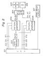
- reference numeral 201 indicates a central processing unit (CPU)
- reference numeral 202 indicates a data memory for storing rectangular patterns such as the rectangular pattern illustrated in Fig. lA or Fig. 1B. That is, in this case, the data memory 202 stores terminal coordinate information (X 0 , Y 0 ) and size information (X 1 , Y l ).
- Reference numerals 203A and 203B indicate pattern generators.
- the pattern generator 203A generates terminal coordinate information (x 0 , y ) and size information (S x , S Y ) as parameters corresponding to each divided pattern illustrated in Fig. 1A to a driver circuit 204.
- the pattern generator 203B generates parameters x 0 , y 0 , S x , and S Y corresponding to each divided pattern illustrated in Fig. 1B to the driver circuit 204.
- the driver circuit 204 drives a main deflection lens 205 and a slit deflection lens 206 to determine the beam positions x 0 and y 0 and the beam size S X and S Y .
- a stage-driver control circuit 207 is used for moving a stage of the electron-beam exposure system.
- the operation of the pattern generator 203A is initiated by a start signal ST1 of the CPU 201 and proceeds with the pulses of a system clock signal CKl.
- the pattern generator 203A When exposure of the divided patterns illustrated in Fig. 1A is conpleted, the pattern generator 203A generates an exposure end signal ED1 which is transmitted to the CPU 201.
- the CPU 201 generates a start signal ST2 to initiate operation of the pattern generator 203B which proceeds with the pulses of a system clock signal CK2.
- the pattern generator 203B When exposure of the divided patterns illustrated in F ig. 1B is completed, the pattern generator 203B generates an exposure end signal ED2 which is transmitted to the CPU 201.
- the CPU 201 proceeds to expose the next rectangular pattern stored in the data memory 202.
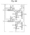
- a register 301 and an adder 302 are provided in order to generate X-direction coordinate information x 0 of a terminal point of a divided pattern
- a register 303 and an adder 304 are provided in order to generate Y-direction coordinate information y 0 of a terminal point of a divided pattern.
- a register 305 a subtracter 306, a comparator 307, and a selector 308 are provided in order to generate size information S x in the X-direction of a divided pattern
- a register 309, a subtracter 310, a comparator 311, and a selector 312 are provided in order to generate size information S y in the Y-direction of a divided pattern.
- the CPU 201 generates a start signal STl, and parameters X 0 , Y 0 , X 1 , and Y 1 are supplied from the data memory 202 to the registers 301, 303, 305, and 309, respectively.
- the comparator 307 compares X 1 with the maximum size S.
- the comparator 311 compares Y 1 with the maximum size S.
- the CPU 201 After the driver circuit 204 exposes the pattern O with a predetermined dose, the CPU 201 generates a pulse of the system clock signal CKl. As a result, the pattern generator 203A performs an operation for generating the pattern 1 of the parameters shown in Fig. l A . That is, the value of the register 301 is changed by the adder 302 from X 0 to X 0 + S. In addition, the value of the register 305 is changed by the subtracter 306 from Y 1 to Y 1 - S. In this case, the outputs of the comparators 307 and 311 remain unchanged. Therefore,
- the pattern 1 of the parameters (x 0 , y 0 , S X , Sy) is (X 0 + S, Y 0 , S, S).
- the pattern generator 203A performs an operation for generating the pattern 6 of the parameters (x 0 , y 0 , S x , Sy) shown in Fig. 1A so that the pattern 6 of the parameters is ( X O + 6S, Y 0 , X 1 - 6S, S).
- the pattern generator 203A performs an operation for generating the pattern 20 of the parameters (x 0 , y 0 , S x , S y ) shown in Fig. 1A so that the pattern 20 of the parameters is ( X O + 6S, Y 0 + 2S , X 1 - 6S, Y 1 - 2S).
- Fig. 4 which illustrates the pattern generator 203B of Fig. 2
- selectors 401 through 404 are added to the elements of Fig. 3. That is, the selectors 401 and 402 are provided so that the first change amount of each of the parameters x 0 and y 0 is set as S/2, not as S, and the selectors 403 and 404 are provided so that the first comparison reference value of each of the comparators 307 and 311 is set as S/2, not as S.
- the CPU 201 generates a start signal ST2, and parameters X 0 , Y 0 , X 1 , and Y 1 are supplied from the data memory 202 to the registers 301, 303, 305, and 309, respectively.
- the comparator 311 compares Y 1 with S/2.
- the CPU 201 After the driver circuit 204 exposes the pattern 0' with a predetermined electron-beam dose, the CPU 201 generates a pulse of the system clock CK2. As a result, the pattern aenerator 203B performs, an operation for generating the pattern 1' of the parameters shown in Fig. 1B. That is, the value of the register 301 is changed by the adder 302 from X 0 to Y 0 + S/2. In addition, the value of the register 305 is changed by the subtracter 306 fron Y 1 to Y l - s/2. In this case, the outputs of the comparators 307 and 311 remain unchanged. However, the selector 403 selects the value S. Therefore,
- the pattern 1' of the parameters (x , y 0 , S X , S Y ) is ( X O + S, Y 0 , S, S/2).
- the pattern generator 203B performs an operation for generating the pattern 6' of the parameters (x 0 , y 0 , S x , S y) shown in Fig. 1B so that the pattern 6' of the parameters is (X O + 11/2S, Y 0 , X 1 - 11/2S, S).
- the selectors 308 and 312 select the lower inputs S/2 thereof. Therefore, the pattern 7' of the parameters (x 0 , y 0 , S X , S Y ) is (X 0 , Y 0 + S, S/2, S).
- the pattern generator 203B performs an operation for generating the pattern 20' of the parameters (x 0 , y 0 , S x , Sy) shown in Fig. 1B so that the pattern 20' of the parameters is
- the shift quantities ir the X- and Y-directions between the two kinds of divided patterns are both S/2.
- shift quantities can be other values only when both the X-direction and the Y-direction are shifted.
- deviation of the border of patterns can be protected against.
Landscapes
- Chemical & Material Sciences (AREA)
- Engineering & Computer Science (AREA)
- Nanotechnology (AREA)
- Analytical Chemistry (AREA)
- Physics & Mathematics (AREA)
- Crystallography & Structural Chemistry (AREA)
- Condensed Matter Physics & Semiconductors (AREA)
- General Physics & Mathematics (AREA)
- Manufacturing & Machinery (AREA)
- Mathematical Physics (AREA)
- Theoretical Computer Science (AREA)
- Electron Beam Exposure (AREA)
Applications Claiming Priority (2)
| Application Number | Priority Date | Filing Date | Title |
|---|---|---|---|
| JP111534/82 | 1982-06-30 | ||
| JP57111534A JPS593923A (ja) | 1982-06-30 | 1982-06-30 | 電子ビ−ム露光方法 |
Publications (3)
| Publication Number | Publication Date |
|---|---|
| EP0098177A2 true EP0098177A2 (de) | 1984-01-11 |
| EP0098177A3 EP0098177A3 (en) | 1986-06-04 |
| EP0098177B1 EP0098177B1 (de) | 1989-03-22 |
Family
ID=14563780
Family Applications (1)
| Application Number | Title | Priority Date | Filing Date |
|---|---|---|---|
| EP83303812A Expired EP0098177B1 (de) | 1982-06-30 | 1983-06-30 | Raster-Elektronenstrahl-Belichtungssystem |
Country Status (3)
| Country | Link |
|---|---|
| EP (1) | EP0098177B1 (de) |
| JP (1) | JPS593923A (de) |
| DE (1) | DE3379487D1 (de) |
Cited By (5)
| Publication number | Priority date | Publication date | Assignee | Title |
|---|---|---|---|---|
| EP0297247A1 (de) * | 1987-06-30 | 1989-01-04 | International Business Machines Corporation | Verfahren zur Elektronenstrahlaufzeichnung und System in Verbindung mit kontinuierlich verschiebbarem Tisch unter Verwendung von Gross-Bereichsablenkung |
| EP0298275A3 (en) * | 1987-07-08 | 1990-06-06 | International Business Machines Corporation | Pattern splicing system and method for scanning of electron beam system |
| EP0433993A3 (en) * | 1989-12-21 | 1991-10-30 | Fujitsu Limited | Method and apparatus for controlling charged particle beams in charged particle beam exposure system |
| EP0688036A3 (de) * | 1994-06-16 | 1997-11-26 | Nikon Corporation | Muster-Übertragungsverfahren mittels einem Ladungsträgerstrahls |
| EP0653103A4 (de) * | 1993-05-28 | 1998-12-16 | Etec Systems Inc | Dosis modulierung und pixel-ablenkung für rasterabgetastetes lithographieverfahren. |
Families Citing this family (1)
| Publication number | Priority date | Publication date | Assignee | Title |
|---|---|---|---|---|
| JPH01286310A (ja) * | 1988-05-12 | 1989-11-17 | Nec Corp | 荷電ビーム露光方法 |
Family Cites Families (4)
| Publication number | Priority date | Publication date | Assignee | Title |
|---|---|---|---|---|
| US4099062A (en) * | 1976-12-27 | 1978-07-04 | International Business Machines Corporation | Electron beam lithography process |
| JPS5493364A (en) * | 1977-12-30 | 1979-07-24 | Fujitsu Ltd | Exposure system for electron beam |
| JPS5831728B2 (ja) * | 1979-12-04 | 1983-07-08 | 日本電子株式会社 | 電子線露光方法 |
| DE3169257D1 (en) * | 1980-11-28 | 1985-04-18 | Ibm | Electron beam system and method |
-
1982
- 1982-06-30 JP JP57111534A patent/JPS593923A/ja active Granted
-
1983
- 1983-06-30 EP EP83303812A patent/EP0098177B1/de not_active Expired
- 1983-06-30 DE DE8383303812T patent/DE3379487D1/de not_active Expired
Cited By (6)
| Publication number | Priority date | Publication date | Assignee | Title |
|---|---|---|---|---|
| EP0297247A1 (de) * | 1987-06-30 | 1989-01-04 | International Business Machines Corporation | Verfahren zur Elektronenstrahlaufzeichnung und System in Verbindung mit kontinuierlich verschiebbarem Tisch unter Verwendung von Gross-Bereichsablenkung |
| EP0298275A3 (en) * | 1987-07-08 | 1990-06-06 | International Business Machines Corporation | Pattern splicing system and method for scanning of electron beam system |
| EP0433993A3 (en) * | 1989-12-21 | 1991-10-30 | Fujitsu Limited | Method and apparatus for controlling charged particle beams in charged particle beam exposure system |
| EP0653103A4 (de) * | 1993-05-28 | 1998-12-16 | Etec Systems Inc | Dosis modulierung und pixel-ablenkung für rasterabgetastetes lithographieverfahren. |
| EP0688036A3 (de) * | 1994-06-16 | 1997-11-26 | Nikon Corporation | Muster-Übertragungsverfahren mittels einem Ladungsträgerstrahls |
| EP0949655A3 (de) * | 1994-06-16 | 2001-04-04 | Nikon Corporation | Musterübertragungsverfahren mittels Ladungsträgerstrahls |
Also Published As
| Publication number | Publication date |
|---|---|
| EP0098177A3 (en) | 1986-06-04 |
| JPS593923A (ja) | 1984-01-10 |
| JPH0341974B2 (de) | 1991-06-25 |
| DE3379487D1 (en) | 1989-04-27 |
| EP0098177B1 (de) | 1989-03-22 |
Similar Documents
| Publication | Publication Date | Title |
|---|---|---|
| KR100330074B1 (ko) | 하전입자선 노광방법 및 웨이퍼상에 패턴을 형성하는 방법 | |
| US6433348B1 (en) | Lithography using multiple pass raster-shaped beam | |
| EP1060498B1 (de) | Verfahren und vorrichtung zur festlegung der formeinkodierung einen ladungsträgerstrahls in lithographie systemen | |
| EP1070335B1 (de) | Gerasterter strahl, elektonenstrahl-schreibstrategie mittels zweidimensionaler mehrpixel-belichtungsfeld | |
| JPH06132203A (ja) | 荷電粒子ビーム露光方法 | |
| JPH07191199A (ja) | 荷電粒子ビーム露光システム及び露光方法 | |
| JPS63114125A (ja) | 荷電ビ−ム露光装置 | |
| GB2152717A (en) | Pattern data handling system for an electron beam exposure system | |
| JP2002118060A (ja) | 荷電ビーム露光装置、荷電ビーム露光方法、露光データ作成方法、露光データを作成するプログラムを記録したコンピュータ読取り可能な記録媒体、及び、露光データを記録したコンピュータ読取り可能な記録媒体 | |
| EP1060500B1 (de) | Gerät und verfahren zur steuerung einer strahlform in lithographie systemen | |
| US5968686A (en) | Charged-beam exposure mask and charged-beam exposure method | |
| EP0098177A2 (de) | Raster-Elektronenstrahl-Belichtungssystem | |
| US20020104970A1 (en) | Raster shaped beam, electron beam exposure strategy using a two dimensional multipixel flash field | |
| US5874189A (en) | Method of optimizing a chip pattern on a semiconductor wafer | |
| US6352802B1 (en) | Mask for electron beam exposure and method of manufacturing semiconductor device using the same | |
| JP2874688B2 (ja) | マスク及びそれを用いた電子線露光方法 | |
| JP3173162B2 (ja) | 透過マスク板 | |
| US6335127B1 (en) | Charged beam mask having strut wider than charged beam, with shape that matches charged beam | |
| JP3481017B2 (ja) | 荷電粒子ビーム露光装置および該荷電粒子ビーム露光装置の露光データ処理方法 | |
| JP3127851B2 (ja) | 重ね合わせ露光方法 | |
| JP3395695B2 (ja) | マスク描画方法 | |
| KR19990063437A (ko) | 전하입자선 직접드로잉을 위한 직접드로잉 데이터 생성방법, 그리고 직접드로잉 방법 및 장치 | |
| JPH11111584A (ja) | 荷電粒子ビーム露光方法 | |
| JPH06112111A (ja) | 荷電粒子ビーム露光方法及び装置 | |
| JP2000124101A (ja) | 荷電粒子線描画用部分一括パターンの作成方法 |
Legal Events
| Date | Code | Title | Description |
|---|---|---|---|
| PUAI | Public reference made under article 153(3) epc to a published international application that has entered the european phase |
Free format text: ORIGINAL CODE: 0009012 |
|
| AK | Designated contracting states |
Designated state(s): DE FR GB |
|
| PUAL | Search report despatched |
Free format text: ORIGINAL CODE: 0009013 |
|
| AK | Designated contracting states |
Kind code of ref document: A3 Designated state(s): DE FR GB |
|
| 17P | Request for examination filed |
Effective date: 19860624 |
|
| 17Q | First examination report despatched |
Effective date: 19870810 |
|
| GRAA | (expected) grant |
Free format text: ORIGINAL CODE: 0009210 |
|
| AK | Designated contracting states |
Kind code of ref document: B1 Designated state(s): DE FR GB |
|
| REF | Corresponds to: |
Ref document number: 3379487 Country of ref document: DE Date of ref document: 19890427 |
|
| ET | Fr: translation filed | ||
| PLBE | No opposition filed within time limit |
Free format text: ORIGINAL CODE: 0009261 |
|
| 26N | No opposition filed | ||
| PGFP | Annual fee paid to national office [announced via postgrant information from national office to epo] |
Ref country code: FR Payment date: 19960611 Year of fee payment: 14 |
|
| PGFP | Annual fee paid to national office [announced via postgrant information from national office to epo] |
Ref country code: GB Payment date: 19960621 Year of fee payment: 14 |
|
| PGFP | Annual fee paid to national office [announced via postgrant information from national office to epo] |
Ref country code: DE Payment date: 19960627 Year of fee payment: 14 |
|
| PG25 | Lapsed in a contracting state [announced via postgrant information from national office to epo] |
Ref country code: GB Free format text: LAPSE BECAUSE OF NON-PAYMENT OF DUE FEES Effective date: 19970630 |
|
| GBPC | Gb: european patent ceased through non-payment of renewal fee |
Effective date: 19970630 |
|
| PG25 | Lapsed in a contracting state [announced via postgrant information from national office to epo] |
Ref country code: FR Free format text: LAPSE BECAUSE OF NON-PAYMENT OF DUE FEES Effective date: 19980227 |
|
| PG25 | Lapsed in a contracting state [announced via postgrant information from national office to epo] |
Ref country code: DE Free format text: LAPSE BECAUSE OF NON-PAYMENT OF DUE FEES Effective date: 19980303 |
|
| REG | Reference to a national code |
Ref country code: FR Ref legal event code: ST |
|
| REG | Reference to a national code |
Ref country code: FR Ref legal event code: ST |