EP0098215A2 - Halbleiterspeicheranordnung - Google Patents
Halbleiterspeicheranordnung Download PDFInfo
- Publication number
- EP0098215A2 EP0098215A2 EP83401300A EP83401300A EP0098215A2 EP 0098215 A2 EP0098215 A2 EP 0098215A2 EP 83401300 A EP83401300 A EP 83401300A EP 83401300 A EP83401300 A EP 83401300A EP 0098215 A2 EP0098215 A2 EP 0098215A2
- Authority
- EP
- European Patent Office
- Prior art keywords
- transistor
- constant current
- current source
- side transistor
- voltage
- Prior art date
- Legal status (The legal status is an assumption and is not a legal conclusion. Google has not performed a legal analysis and makes no representation as to the accuracy of the status listed.)
- Granted
Links
Images


Classifications
-
- G—PHYSICS
- G11—INFORMATION STORAGE
- G11C—STATIC STORES
- G11C5/00—Details of stores covered by group G11C11/00
- G11C5/14—Power supply arrangements, e.g. power down, chip selection or deselection, layout of wirings or power grids, or multiple supply levels
-
- G—PHYSICS
- G11—INFORMATION STORAGE
- G11C—STATIC STORES
- G11C17/00—Read-only memories programmable only once; Semi-permanent stores, e.g. manually-replaceable information cards
- G11C17/14—Read-only memories programmable only once; Semi-permanent stores, e.g. manually-replaceable information cards in which contents are determined by selectively establishing, breaking or modifying connecting links by permanently altering the state of coupling elements, e.g. PROM
- G11C17/18—Auxiliary circuits, e.g. for writing into memory
Definitions
- the present invention relates to a semiconductor memory device, more particularly to control circuits included in a semiconductor memory device which is preferably fabricated as a programmable read only memory (PROM).
- a semiconductor memory device which is preferably fabricated as a programmable read only memory (PROM).
- the present invention mainly refers to a PROM.
- a bit selection, word selection, and read operation are achieved under a power source voltage of V .
- a program control voltage V p is needed which exceeds.the level of V cc , for example, 20 V.
- a PROM is usually supplied for commercial sale in a standard one-chip package. Therefore, the number of input/output pins is limited. Because of this, a pin may often have to be commonly used as a terminal for two or more different input/output signals. Such common use of a pin poses no problem if the input/output signals have the same voltage levels. However, there is a problem if a pin is commonly used as an input terminal for both a program control voltage V p and a usual input control signal S having a voltage of V sc .
- a switching circuit must be employed so as to prevent malfunctions in the constant current source which drives the program circuits connected to the common use pin. That is, the switching circuit operates to transfer the desired program control voltage V p to the constant current source and the program circuits selectively only when the program control voltage V p is applied to the pin.
- the present invention specifically relates to such a switching circuit.
- the above object is attained by a switching circuit which further operates, while maintaining its inherent function, to prevent application of the power source voltage of V cc to a line between the common use pin and both the constant current source and the program circuits during the read operation of the memory, so that, even if channel leakage occurs in the transistor of the constant current source, the transistor cannot be turned on.
- the present invention relates to a switching circuit. Therefore, first the location of a switching circuit in a PROM will be clarified.
- Figure 1 is a circuit diagram of a prior art PROM of a junction shorting type.
- reference numerals 11 indicate bit lines, 12 word lines, and 13 memory cells arranged at each cross point of the bit line and the word line.
- the data of each memory cell 13 is not erasable once a write operation is achieved therein.
- the desired memory cell 13 is selected by selecting the corresponding bit line 11 by means of a bit decoder 14-2 and selecting the corresponding word line 12 by means of a word decoder 15.
- bit address AD b and word address AD w are applied, respectively.
- the bit decoder 14-2 is used for a data reading operation.
- the read data for the corresponding bit line is produced, via an OR gate 16 and an output buffer 17, from an input/output terminal 18.
- a write mode is performed as follows.
- One of program circuits 21 to which the data is to be written is selected by a bit decoder 14-1 in accordance with the bit address AD b .
- a program current of about 120 mA is supplied, via a switching circuit 24', from the. input/output terminal 18 to the thus selected program circuit 21 and further to the corresponding bit line 11.
- a Schottky barrier diode 22 is inserted in each bit line 11 so as to prevent any deleterious effect by the program current to the circuit for achieving the read operation.
- the program circuit 21 is formed as a Darlington circuit so that the program current of 120 mA can flow therethrough.
- a so-called constant current source 23 is employed therefor.
- the constant current source 23 is made active only during the write operation mode. That is, the source 23 is not activated until the program control voltage V p of about 20 V is applied to a control terminal 25.
- the source 23 must electrically effective viewed from the control terminal 25 under the write operation mode only and, while must not be electrically effective viewed therefrom under any mode other than the write operation mode. For this, a switching circuit is required.
- the inventors have attempted to employ a circuit 24 as that swiching circuit.
- the switching circuit 24 at the side of the control terminal 25 has a similar construction to the switching circuit 24' at the side of the input/output terminal 18, which switching circuit 24' has already been known, for example, as recited in a catalog by INTERSIL, INC as "IM56SXX SERIES". It should be noted that the function to be performed by the switching circuit 24 is quite different from that of the switching circuit 24'.
- control terminal 25 is a common terminal for selectively receiving the program control voltage V under the write operation mode or the input control signal S under the read operation mode.
- input control signal S is used, for exmaple, as a signal to activate the output buffer 17 via a chip enable circuit CE, during the read operation mode.
- the signal S c is not limited to such a signal as above, but can be used for other purposes.
- the program control voltage V or the input control signal S c is selectively applied to the control terminal 25.
- the constant current source 23 and the related circuits cannot be electrically effective viewed from the input control signal S c , however, is electrically effective viewed from the control terminal 25 only when the program voltage V is applied thereto. This is made possible by means of the switching circuit 24.
- the circuit 24 is comprised of a diode 31 and a Schottky barrier diode 32.
- the diode 31 is fully cut off when a signal having a level lower than V cc such as the input control signal S c , is applied to the terminal 25, because a parasitic capacitor 33, at the cathode side of the diode 31, has charged up to the power source voltage level of V cc through the diode 32. Consequently, only a junction capacitor 34 of the diode 31 is visible for the input control signal S c .
- control circuits to which the present invention is concerned are specifically the program circuits 21, the constant current source 23, and the switching circuit 24.
- the circuits 21 and the source 23 are already known, for example, in Fig. 4 of U.S. Patent 4,319,341.
- the transistor 36 is preferrably formed with a lateral PNP structure. If the transistor 36 is so formed, there is a possibility that the transistor 36 will be unintentionally turned on during the read operation mode.
- impurities (+ ion) may originally be included therein or externally injected thereinto after formation of the insulation layer. Such impurities may often change the conduction type at the surface of the base region to a P type, in which it is considered that the impurities of + ion are charged at the upper side of the insulation layer, while the impurities of - ion are charged at the bottom side thereof. Therefore, a P type channel attracted by impurities of - ion is created in the surface of the base region. It should be noted that the lateral PNP transistor 36 is advantageous for simply constructing the constant current source 23.
- the insulation layer is covered by an emitter electrode, which insulation layer is formed on the base region. Since the emitter electrode is maintained at the power source voltage level of V cc , the - ion impurities are attracted to the upper side of the insulation layer, and, therefore, the + ion impurities are charged at the bottom side thereof. The thus charged + ion impurities change the conduction type of the channel to the N type. As a result, undesired channel leakage can be avoided.
- Figure 2A is a plan view of a lateral PNP transistor with an emitter electrode for avoiding channel leakage.
- Figure 2B is a cross--sectional view taken along the line 2B-2B in Fig. 2A.
- Figure 3A is a plan view of a lateral PNP transistor with a usual emitter electrode.
- Figure 3B is a cross--sectional view taken along the line 3B-3B in Fig. 3A.
- the concerned transistor 36 in Fig. 1 has a plan view and a cross-sectional view shown in Figs. 2A and 2B, respectively.
- Figs. 2A and 2B particular attention should be paid to an emitter electrode EE.
- the electrode EE is wider than a usual emitter electrode EE' of Figs. 3A and 3B and covers the base region B. Thus, channel leakage can be prevented.
- reference symbol IL denotes the insulation layer mentioned hereinbefore, Cl a first collector region, C2 a second collector region, CE1 a first collector electrode, and CE2 a second collector electrode.
- the disadvantage of the prior art is that, as clear from Figs. 2A and 2B, the empolyment of such a wide emitter electrode EE impedes realization of a highly integrated memory. That is, the collector electrodes CE1 and CE2 of Figs. 2A and 2B must be positioned far enough from the adjacent emitter electrode EE to prevent electric shorting between these electrodes CE1, CE2 and EE. In this regard, the transistor 36 occupies a considerably large area in the memory.
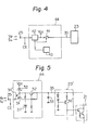
- FIG. 4 is a circuit diagram of a principle of a switching circuit included in the memory according to the present invention.
- a switching circuit 44 corresponds to the prior art switching circuit 24 shown in Fig. 1.
- Other members 23, 25, and 35 are identical to the constant current source, control terminal, and line, respectively.
- the switching circuit 44 includes therein a switching element 41 which receives, at its input side, the power source voltage V . Accordingly, so long as the switching element 41 is held off, no power source voltage V cc can be applied to the transistor 36 (Fig. 1) in the constant current source 23. This means that, even if the aforesaid channel leakage occurs in the transistor 36, there is no possibility that the base current will be supplied to the first stage transistor of each program circuit 21 (Fig. 1).
- the on-off driving for the switching element 41 is achieved by an on-off driving circuit 42.
- the circuit 42 is controlled by a voltage detecting element 43.
- a signal to be applied to the control terminal 25 is the usual input control signal S c
- the circuit 42 functions to place off the switching element 41.
- the program control voltage V is applied to the control terminal 25
- the voltage detecting element 43 detects the applied voltage level of, for example, 20 V.
- the circuit 42 functions such as to place on the switching element 41. This makes the constant current source 23 active, and thereby the program circuit 21 (Fig. 1), connected to the selected bit line 11 by the address AD b , is operated.
- FIG. 5 is a detailed circuit diagram of the switching circuit 44 of Fig. 4 and its neighboring control circuits.
- the switching element 41 of Fig. 4 is formed by, for exmple an output side transistor 52, as illustrated therein.
- the transistor 52 and an input side transistor 51 together with the voltage detecting element are constructed, as a whole, in the form of a thyristor.
- the thyristor structure is not intentionally formed, but necessarily results from the above-mentioned transistor arrangement. There is no reason for intentionally introducing such a thyristor.
- the voltage detecting element 43 (Fig. 4) is made of the Zener diode 37.
- the Zener diode 37 is not newly empolyed, but is one removed from the constant current source 23 of Fig. 1, which Zener voltage is, for exmaple 6 V. Thus, no Zener diode similar to that of the constant current source 23 in Fig. 1 is found in the corresponding constant current source 23' in Fig. 5.
- the transistor 51 can be turned on if a trigger current flows from the control terminal 25 via the emitter and base of the transistor 51 and the Zener diode 37 to the ground.
- the transistor 51 cannot be turned on, and the input control signal S is of the voltage V SC , which level merely reaches the Zener region of the Zener diode 37. Therefore, the transistor 52 is also still off.
- the input side transistor 51 to be connected to the control terminal 25 is preferably fabricated as a lateral PNP transistor, as is the transistor 36'. Further, the lateral PNP transistor 51 is preferably formed to have the enlarged emitter electrode as shown in Figs. 2A and 2B so as to prevent channel leakage. It should be noted that the employment of such a lateral PNP transistor 51 having an enlarged emitter electrode does not cause a problem in the integration of the memory. This is because there is only one transistor 51 in the memory. It should be noted that the above mentioned matters do not apply to the transistor 52, because it is an NPN type transistor.
- the high level program voltage V is applied to the control terminal 25. Therefore, the trigger current flows through the emitter and base of the transistor 51 and the diode 37. The transistor 51 is turned on by the trigger current. Soon after this, a base current is supplied to the output side transistor 52 from the transistor 51 now on. Thus, the transistor 52 is also turned on. Once both transistors 51 and 52 are turned on, the on state is held without the aforesaid trigger current. However, the transistors 51 and 52 are turned off when the program voltage V stops being applied to the terminal 25. If no program voltage V p is given, the transistors 51 and 52 are both off.
- each transistor 36' is guaranteed to be off during the read operation mode. Consequently, it is not necessary to form each transistor 36' as shown in Figs. 2A and 2B. They can be formed as shown in Figs. 3A and 3B. This makes it possible to reduce the size of each transistor 36'.
Landscapes
- Engineering & Computer Science (AREA)
- Power Engineering (AREA)
- Read Only Memory (AREA)
Applications Claiming Priority (2)
| Application Number | Priority Date | Filing Date | Title |
|---|---|---|---|
| JP57111536A JPS5922295A (ja) | 1982-06-30 | 1982-06-30 | 半導体記憶装置 |
| JP111536/82 | 1982-06-30 |
Publications (3)
| Publication Number | Publication Date |
|---|---|
| EP0098215A2 true EP0098215A2 (de) | 1984-01-11 |
| EP0098215A3 EP0098215A3 (en) | 1987-05-13 |
| EP0098215B1 EP0098215B1 (de) | 1992-05-06 |
Family
ID=14563836
Family Applications (1)
| Application Number | Title | Priority Date | Filing Date |
|---|---|---|---|
| EP83401300A Expired - Lifetime EP0098215B1 (de) | 1982-06-30 | 1983-06-23 | Halbleiterspeicheranordnung |
Country Status (5)
| Country | Link |
|---|---|
| US (1) | US4599688A (de) |
| EP (1) | EP0098215B1 (de) |
| JP (1) | JPS5922295A (de) |
| DE (1) | DE3382555D1 (de) |
| IE (1) | IE58553B1 (de) |
Cited By (8)
| Publication number | Priority date | Publication date | Assignee | Title |
|---|---|---|---|---|
| US4734885A (en) * | 1985-10-17 | 1988-03-29 | Harris Corporation | Programming arrangement for programmable devices |
| FR2608826A1 (fr) * | 1986-12-19 | 1988-06-24 | Eurotechnique Sa | Circuit integre comportant des elements d'aiguillage vers des elements de redondance dans une memoire |
| FR2632110A1 (fr) * | 1988-05-27 | 1989-12-01 | Bendix Electronics Sa | Procede et dispositif de programmation d'une memoire du type prom et memoire en faisant application |
| EP0229081A4 (de) * | 1985-07-09 | 1990-03-22 | Motorola Inc | Anpassungsfähiges zeilentreiberschaltung und ausgangsschaltung für programmierbaren nur-lese-speicher. |
| US4958324A (en) * | 1987-11-24 | 1990-09-18 | Sgs-Thomson Microelectronics Sa | Method for the testing of electrically programmable memory cells, and corresponding integrated circuit |
| EP0019381B1 (de) * | 1979-04-27 | 1991-01-09 | Fujitsu Limited | Halbleiterspeicher mit Adressensignalpegeleinstellung |
| EP0357502A3 (de) * | 1988-08-30 | 1992-01-02 | Fujitsu Limited | Programmierbare Halbleiterspeicherschaltung |
| FR2666913A1 (fr) * | 1990-09-19 | 1992-03-20 | Samsung Electronics Co Ltd | Circuit de regulation de courant dans une ram statique. |
Families Citing this family (3)
| Publication number | Priority date | Publication date | Assignee | Title |
|---|---|---|---|---|
| JPS61150199A (ja) * | 1984-12-25 | 1986-07-08 | Nec Corp | 半導体記憶装置 |
| US5498562A (en) * | 1993-04-07 | 1996-03-12 | Micron Technology, Inc. | Semiconductor processing methods of forming stacked capacitors |
| JP6265295B1 (ja) | 2017-06-14 | 2018-01-24 | Smk株式会社 | コンタクト |
Citations (1)
| Publication number | Priority date | Publication date | Assignee | Title |
|---|---|---|---|---|
| US4319341A (en) | 1979-04-25 | 1982-03-09 | Fujitsu Limited | Programming circuit for permanently storing data in a programmable read only memory |
Family Cites Families (5)
| Publication number | Priority date | Publication date | Assignee | Title |
|---|---|---|---|---|
| JPS55140265A (en) * | 1979-04-13 | 1980-11-01 | Fujitsu Ltd | Semiconductor memory device and method of fabricating the same |
| JPS55142475A (en) * | 1979-04-23 | 1980-11-07 | Fujitsu Ltd | Decoder circuit |
| JPS5828680B2 (ja) * | 1979-04-27 | 1983-06-17 | 富士通株式会社 | 半導体記憶装置 |
| JPS606040B2 (ja) * | 1979-06-07 | 1985-02-15 | 日本電気株式会社 | 集積回路 |
| JPS57143798A (en) * | 1981-03-02 | 1982-09-06 | Fujitsu Ltd | Programmable element |
-
1982
- 1982-06-30 JP JP57111536A patent/JPS5922295A/ja active Granted
-
1983
- 1983-06-23 EP EP83401300A patent/EP0098215B1/de not_active Expired - Lifetime
- 1983-06-23 DE DE8383401300T patent/DE3382555D1/de not_active Expired - Lifetime
- 1983-06-28 US US06/508,544 patent/US4599688A/en not_active Expired - Fee Related
- 1983-06-30 IE IE154183A patent/IE58553B1/en not_active IP Right Cessation
Patent Citations (1)
| Publication number | Priority date | Publication date | Assignee | Title |
|---|---|---|---|---|
| US4319341A (en) | 1979-04-25 | 1982-03-09 | Fujitsu Limited | Programming circuit for permanently storing data in a programmable read only memory |
Cited By (10)
| Publication number | Priority date | Publication date | Assignee | Title |
|---|---|---|---|---|
| EP0019381B1 (de) * | 1979-04-27 | 1991-01-09 | Fujitsu Limited | Halbleiterspeicher mit Adressensignalpegeleinstellung |
| EP0229081A4 (de) * | 1985-07-09 | 1990-03-22 | Motorola Inc | Anpassungsfähiges zeilentreiberschaltung und ausgangsschaltung für programmierbaren nur-lese-speicher. |
| US4734885A (en) * | 1985-10-17 | 1988-03-29 | Harris Corporation | Programming arrangement for programmable devices |
| FR2608826A1 (fr) * | 1986-12-19 | 1988-06-24 | Eurotechnique Sa | Circuit integre comportant des elements d'aiguillage vers des elements de redondance dans une memoire |
| EP0275752A1 (de) * | 1986-12-19 | 1988-07-27 | Sgs-Thomson Microelectronics S.A. | Integrierte Schaltung mit Weichenelementen nach redundanten Elementen in einem Speicher |
| US4860256A (en) * | 1986-12-19 | 1989-08-22 | Sgs-Thomson Microelectronics S.A. | Integrated circuit provided with switching elements for changeover to redundancy elements in a memory |
| US4958324A (en) * | 1987-11-24 | 1990-09-18 | Sgs-Thomson Microelectronics Sa | Method for the testing of electrically programmable memory cells, and corresponding integrated circuit |
| FR2632110A1 (fr) * | 1988-05-27 | 1989-12-01 | Bendix Electronics Sa | Procede et dispositif de programmation d'une memoire du type prom et memoire en faisant application |
| EP0357502A3 (de) * | 1988-08-30 | 1992-01-02 | Fujitsu Limited | Programmierbare Halbleiterspeicherschaltung |
| FR2666913A1 (fr) * | 1990-09-19 | 1992-03-20 | Samsung Electronics Co Ltd | Circuit de regulation de courant dans une ram statique. |
Also Published As
| Publication number | Publication date |
|---|---|
| IE58553B1 (en) | 1993-10-06 |
| US4599688A (en) | 1986-07-08 |
| EP0098215B1 (de) | 1992-05-06 |
| EP0098215A3 (en) | 1987-05-13 |
| JPS6137717B2 (de) | 1986-08-25 |
| DE3382555D1 (de) | 1992-06-11 |
| IE831541L (en) | 1983-12-30 |
| JPS5922295A (ja) | 1984-02-04 |
Similar Documents
| Publication | Publication Date | Title |
|---|---|---|
| EP0499110B1 (de) | Schalter zur Verwendung in einer integrierten Schaltung | |
| US4404659A (en) | Programmable read only memory | |
| US4347586A (en) | Semiconductor memory device | |
| US4599688A (en) | Semiconductor memory device having switching circuit for preventing channel leakage in constant current source | |
| US4174541A (en) | Bipolar monolithic integrated circuit memory with standby power enable | |
| US4319341A (en) | Programming circuit for permanently storing data in a programmable read only memory | |
| US4130889A (en) | Programmable write-once, read-only semiconductor memory array using SCR current sink and current source devices | |
| US5138142A (en) | Ic card with improved power supply switching circuitry | |
| JP2852391B2 (ja) | フューズ溶断装置 | |
| EP0140368B1 (de) | Mit Prüfzellen ausgestattetes programmierbares ROM-Gerät | |
| EP0019381B1 (de) | Halbleiterspeicher mit Adressensignalpegeleinstellung | |
| US4656609A (en) | Semiconductor memory device | |
| US4432070A (en) | High speed PROM device | |
| US4638466A (en) | Programmable semiconductor memory device having separate read word line drivers and write-only word line drivers | |
| EP0018192A1 (de) | Programmierbare, mit Adressierschaltungen versehene, bipolare Festwertspeichervorrichtung | |
| US4488261A (en) | Field programmable device | |
| EP0028157B1 (de) | Integrierte Halbleiterspeicherschaltung mit integrierter Injektionslogik | |
| EP0098142B1 (de) | Programmierbare Festwertspeicheranordnungen | |
| KR20040068225A (ko) | 반밀도 롬 내장형 디램 | |
| US5650956A (en) | Current amplification type mask-ROM | |
| EP0263318B1 (de) | Halbleiterspeicher | |
| US4593383A (en) | Integated circuit memory | |
| US4891683A (en) | Integrated SCR current sourcing sinking device | |
| US4729116A (en) | Bipolar programmable read only memory attaining high speed data read operation | |
| US3475735A (en) | Semiconductor memory |
Legal Events
| Date | Code | Title | Description |
|---|---|---|---|
| PUAI | Public reference made under article 153(3) epc to a published international application that has entered the european phase |
Free format text: ORIGINAL CODE: 0009012 |
|
| AK | Designated contracting states |
Designated state(s): DE FR GB |
|
| PUAL | Search report despatched |
Free format text: ORIGINAL CODE: 0009013 |
|
| AK | Designated contracting states |
Kind code of ref document: A3 Designated state(s): DE FR GB |
|
| 17P | Request for examination filed |
Effective date: 19870827 |
|
| 17Q | First examination report despatched |
Effective date: 19880405 |
|
| GRAA | (expected) grant |
Free format text: ORIGINAL CODE: 0009210 |
|
| AK | Designated contracting states |
Kind code of ref document: B1 Designated state(s): DE FR GB |
|
| REF | Corresponds to: |
Ref document number: 3382555 Country of ref document: DE Date of ref document: 19920611 |
|
| ET | Fr: translation filed | ||
| PLBE | No opposition filed within time limit |
Free format text: ORIGINAL CODE: 0009261 |
|
| STAA | Information on the status of an ep patent application or granted ep patent |
Free format text: STATUS: NO OPPOSITION FILED WITHIN TIME LIMIT |
|
| PGFP | Annual fee paid to national office [announced via postgrant information from national office to epo] |
Ref country code: GB Payment date: 19930408 Year of fee payment: 11 |
|
| 26N | No opposition filed | ||
| PGFP | Annual fee paid to national office [announced via postgrant information from national office to epo] |
Ref country code: FR Payment date: 19930629 Year of fee payment: 11 |
|
| PGFP | Annual fee paid to national office [announced via postgrant information from national office to epo] |
Ref country code: DE Payment date: 19930830 Year of fee payment: 11 |
|
| PG25 | Lapsed in a contracting state [announced via postgrant information from national office to epo] |
Ref country code: GB Effective date: 19940623 |
|
| GBPC | Gb: european patent ceased through non-payment of renewal fee |
Effective date: 19940623 |
|
| PG25 | Lapsed in a contracting state [announced via postgrant information from national office to epo] |
Ref country code: FR Effective date: 19950228 |
|
| PG25 | Lapsed in a contracting state [announced via postgrant information from national office to epo] |
Ref country code: DE Effective date: 19950301 |
|
| REG | Reference to a national code |
Ref country code: FR Ref legal event code: ST |
|
| APAH | Appeal reference modified |
Free format text: ORIGINAL CODE: EPIDOSCREFNO |