EP0263318B1 - Halbleiterspeicher - Google Patents
Halbleiterspeicher Download PDFInfo
- Publication number
- EP0263318B1 EP0263318B1 EP87113251A EP87113251A EP0263318B1 EP 0263318 B1 EP0263318 B1 EP 0263318B1 EP 87113251 A EP87113251 A EP 87113251A EP 87113251 A EP87113251 A EP 87113251A EP 0263318 B1 EP0263318 B1 EP 0263318B1
- Authority
- EP
- European Patent Office
- Prior art keywords
- data
- column
- writing
- mos transistor
- mos transistors
- Prior art date
- Legal status (The legal status is an assumption and is not a legal conclusion. Google has not performed a legal analysis and makes no representation as to the accuracy of the status listed.)
- Expired - Lifetime
Links
- 239000004065 semiconductor Substances 0.000 title claims description 30
- 230000015654 memory Effects 0.000 claims description 140
- 230000005540 biological transmission Effects 0.000 claims description 10
- 239000011159 matrix material Substances 0.000 claims description 9
- 230000007423 decrease Effects 0.000 claims description 4
- 238000010586 diagram Methods 0.000 description 12
- 239000000758 substrate Substances 0.000 description 12
- 238000000034 method Methods 0.000 description 6
- 238000009413 insulation Methods 0.000 description 4
- XUIMIQQOPSSXEZ-UHFFFAOYSA-N Silicon Chemical compound [Si] XUIMIQQOPSSXEZ-UHFFFAOYSA-N 0.000 description 3
- 230000006870 function Effects 0.000 description 3
- 239000000969 carrier Substances 0.000 description 2
- 238000009792 diffusion process Methods 0.000 description 2
- 229910052710 silicon Inorganic materials 0.000 description 2
- 239000010703 silicon Substances 0.000 description 2
- XAGFODPZIPBFFR-UHFFFAOYSA-N aluminium Chemical compound [Al] XAGFODPZIPBFFR-UHFFFAOYSA-N 0.000 description 1
- 229910052782 aluminium Inorganic materials 0.000 description 1
- 230000000295 complement effect Effects 0.000 description 1
- 230000006866 deterioration Effects 0.000 description 1
- 230000000694 effects Effects 0.000 description 1
- 239000012535 impurity Substances 0.000 description 1
- 230000010354 integration Effects 0.000 description 1
- 238000002955 isolation Methods 0.000 description 1
- 229910021420 polycrystalline silicon Inorganic materials 0.000 description 1
- 239000007787 solid Substances 0.000 description 1
Images


Classifications
-
- G—PHYSICS
- G11—INFORMATION STORAGE
- G11C—STATIC STORES
- G11C16/00—Erasable programmable read-only memories
- G11C16/02—Erasable programmable read-only memories electrically programmable
- G11C16/04—Erasable programmable read-only memories electrically programmable using variable threshold transistors, e.g. FAMOS
- G11C16/0408—Erasable programmable read-only memories electrically programmable using variable threshold transistors, e.g. FAMOS comprising cells containing floating gate transistors
- G11C16/0416—Erasable programmable read-only memories electrically programmable using variable threshold transistors, e.g. FAMOS comprising cells containing floating gate transistors comprising cells containing a single floating gate transistor and no select transistor, e.g. UV EPROM
Definitions
- the present invention relates to a semiconductor memory and, more particularly, to a programmable read-only memory (PROM) into which data can be written.
- PROM programmable read-only memory
- a floating-gate, n-channel MOS transistor used as a memory cell in a programmable read-only memory (PROM) has the structure as shown in Fig. 1.
- source 12 and drain 13, both constituted by N+ diffusion layers, are formed in one major surface region of P-type silicon substrate 11.
- Insulation film 14 is formed on the major surface of substrate 11.
- Floating gate 15 is embedded in insulation film 14 and is located above that portion of substrate 11 which is situated between source 12 and drain 13. Floating gate 15 thus floats electrically above substrate 11.
- Control gate 16 is formed on insulation film 14 and is located above floating gate 15.
- Source electrode 17 is formed in one of two contact holes cut in insulation film 14, and is thereby electrically connected to source 12.
- Drain electrode 18 is formed in the other contact hole, and is thereby electrically connected to drain 13.
- P-type silicon substrate 11 and source 12 are set at the ground potential (GND). Then, a voltage of, for example, 12.5 V is applied to control gate 16, and a voltage of, for example, 7.0 V is applied to drain 13. As a result, the potential of floating gate 15 rises to, for instance, 9.0 V, since 12.5 V, has been applied to control gate 16. Hence, 9.0 V is applied between floating gate 15 and substrate 11, whereby an inversion layer, that is, N-type layer 19, is formed in that surface region of substrate 11 which separates source 12 and drain 13. The electrons within inversion layer 19 are moved toward drain 13 by the voltage applied to drain 13, and collide with those silicon atoms of substrate 11 which are present near drain 13. A so-called "electron avalanche" occurs near drain 13, thereby generating new electrons. Some of these electrons drift to drain 13, and the rest are injected into floating gate 15.
- GND ground potential
- PROM comprising a number of memory cells having the structure as shown in Fig. 1, it is generally required that data be written into each memory cell in the shortest time possible; for example, within 1 millisecond, or within 100 microseconds.
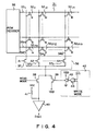
- Fig. 2 shows a circuit consisting of one memory cell 21 of the type shown in Fig. 1, and a circuit for writing data thereinto. Also provided are n-channel MOS transistors 22 and 23, having their current paths connected in series. MOS transistor 22, which is a data-writing transistor, has its drain connected to high-voltage power supply Vpp for supplying 12.5 V, and its gate receives a write signal. MOS transistor 23 is a column-selecting transistor, and its gate receives a column-address signal of voltage Vpp. A row-address signal of voltage Vpp is applied to the control gate of memory cell 21.
- Fig. 3 is a graph illustrating the data-writing characteristic of the semiconductor memory circuit shown in Fig. 2.
- curve I indicates the operation characteristic, i.e., the relationship between the drain current Ids and drain voltage Vds which memory cell 21 exhibits when a voltage of 12.5 V (i.e., voltage Vpp) is applied to its control gate.
- Vpp voltage of 12.5 V
- Curve II represents the way in which the load applied on memory cell 21 changes as current Ids and voltage Vds change.
- Intersection P of curves I and II denotes the operation point of memory cell 21.
- Curve II is specific to a load constituted by an n-channel MOS transistor.
- Data can be written into memory cell 21 even if current Ids is below point T, provided the data does not have to be written at high speed. In order that data can be written in at a sufficiently high speed, drain current Ids should be at the same level as, or above, point T.
- PROMs programmable read-only memories
- a PROM has memory-cell matrix 31, which comprises a floating-gate, and n-channel MOS transistors 32 ll to 32 mn which are used as memory cells.
- the MOS transistors are arranged in rows and columns.
- the control gates of the n-channel MOS transistors forming each row are coupled to a row-signal line. More specifically, MOS transistors 32 ll to 32 ln of the first row have their control gates connected to the first row-signal line 33 l , MOS transistors 32 2l to 32 2n of the second row have their control gates coupled to the second row line 332, and so forth.
- MOS transistors 32 ml to 32 mn of the last row have their control gates coupled to the last row-signal line 33 m . Further, the drains of the MOS transistors forming each column are coupled to a column-signal line. More precisely, MOS transistors 32 ll to 32 ml of the first column have their drains connected to the first column-signal line 34 l , MOS transistors 32 l2 to 32 m2 of the second column have their drains coupled to the second column-signal line 342, and so forth. MOS transistors 32 ln to 32 mn of the last column have their drains connected to the last column-signal line 34 n . The sources of all n-channel MOS transistors 32 ll to 32 mn are connected to the ground.
- the PROM further comprises row decoder 35 and column-selecting circuit 36.
- the output of row decoder 35 is coupled to row-signal lines 33 l to 33 m .
- the column-selecting circuit 36 is connected to column-signal lines 34 l to 34 n .
- Column-selecting circuit 36 comprises column-selecting n-channel MOS transistors 37 l to 37 n , which are turned on and off by outputs A l to A n of a column decoder (not shown).
- MOS transistors 37 l to 37 n are connected at one end to column-signal lines 34 l to 34 n , respectively, and at the other end to one another, thus forming a node.
- Data-reading n-channel MOS transistor 38 and data-writing MOS transistor 39 are each connected at one end to this node.
- the other end of MOS transistor 38 is connected to the input terminal of sense amplifier circuit 40 and also to resistor 41, which in turn is coupled to power supply potential Vcc.
- Data-reading MOS transistor 38 is turned on by a read-mode signal.
- the other end of data-writing MOS transistor 39 is coupled to high-voltage power supply potential Vpp.
- MOS transistor 39 is turned on by the output of data-writing gate circuit 42.
- Gate circuit 42 comprises buffer circuit 43 and AND gate 44.
- Buffer circuit 43 is coupled to power supply potential Vpp, and has an output terminal connected to the gate of data-writing MOS transistor 39.
- AND gate 44 has an output terminal coupled to the input terminal of buffer circuit 43, and provides a logical sum of a write-mode signal and data Din to be written in the PROM.
- Data “0” and data “1” can be written into any desired memory cell.
- MOS transistor 38 When the write-mode signal and the read-mode signal are at level “1" and level “0", respectively, MOS transistor 38 is off.
- data Din is “1”
- the output of AND gate is at level "1”.
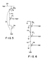
- Fig. 5 shows memory cell 32 ij and the circuit for writing data thereinto.
- the gate potentials of data-writing MOS transistor 39, column-selecting MOS transistor 37 j , and memory cell 32 ij are set at Vpp level (usually 12.5 V), thereby turning these MOS transistors on.
- Current Iw flows from high-voltage power source Vpp, coupled to the drain of MOS transistor 39, to the source (i.e., ground GND) of floating-gate MOS transistor 32 ij used as memory cell 32 ij .
- the hot carriers (i.e., electrons) induced by current I are injected into the floating gate of memory cell 32 ij , thereby writing data "0" thereinto.
- the gate potential of data-writing MOS transistor 39 is set at the GND level.
- MOS transistor 39 is off. Hence, no current flows to memory cell 32 ij from high-voltage power source Vpp. As a result, no electrons are injected into the floating gate of memory cell 32 ij , and this memory cell stores data "1".
- memory cell 32 ij is an n-channel MOS transistor.
- Column-selecting MOS transistor 37 j and data-writing MOS transistor 39 are also n-channel transistors.
- Fig. 6 is a circuit diagram modified from the diagram of Fig. 5, and explains how data "0" is written into memory cell 32 ij .
- Vpp high voltage
- MOS transistor 39 is of enhancement type: Va ⁇ Vpp - V THN where V THN is the threshold voltage of MOS transistor 39.
- Source potential Va is not equal to the substrate voltage (GND), and hence, due to the back-gate bias effect, the apparent threshold voltage of MOS transistor 39 rises, and source potential Va is therefore lower than Vpp - V THN .
- source potential Vb of column-selecting MOS transistor 37 j is approximately equal to source potential Va of MOS transistor 39. It follows that potential Va is applied to the source of memory cell 32 ij . As long as the Vpp level is sufficiently high, source potential Va of MOS transistor 39 is also high, and there is no problem in programming the PROM.
- a semiconductor memory having a non volatile cell, and first and second MOS transistors in series, with the first transistor being of different channel type, is shown in US-A-4 387 444.
- the gates of the cell and the transistors are connected together, and the circuit forms part of a non volatile semiconductor latch.
- EP-A-0 050 005 shows an EPROM device with a memory cell and two MOS transistors in series, but the cell and the transistors are of the same channel type.
- JP-A-61 097 976 shows improving read-out and write-in efficiency in an EPROM composed of a P-channel write transistor and an N-channel read transistor having a common floating gate.
- P-channel MOS transistors for addressing and for switching a programming voltage onto a memory cell is shown in pages 106-107 of the 1978 I EEE Solid State Circuit Conference 16th February 1978, but only in conjunction with P-channel memory cells.
- the data-writing voltage is lowered by the threshold voltage of the data-writing MOS transistor.
- the current flowing through the source-drain path of each memory cell therefore decreases. Consequently, the efficiency of writing data "0" into the memory cell is inevitably low.
- Another object of the present invention is to provide a semiconductor memory wherein sufficient current can be supplied to each memory cell, even if the data-writing voltage is relatively low, so as to ensure that data "0" can be written into the cell at a sufficiently high speed.
- a semiconductor memory comprising: means for connecting a data writing potential; means for connecting a reference potential; a PROM cell, a first MOS transistor and a second MOS transistor connected in series between said data writing potential and said reference potential, wherein the PROM cell is of a first channel type, and is electrically programmable to store data therein; the first MOS transistor is of a second channel type; characterized in that a gate of said PROM cell receives a row selection signal; a gate of said first MOS transistor receives a write signal to determine the operation point of said PROM cell when the memory is set in a data-writing mode; and the second MOS transistor is of said second channel type, and a gate of said second MOS transistor receives a column selection signal to decrease time required for writing data into said PROM cell; and further comprising means for generating and supplying said row selection signal to the gate of said PROM cell; means for generating and supplying said write signal to the gate of said first MOS transistor; and means for
- Opposite channel type MOS transistors are connected together, so that the opposite channel type MOS transistor functions as the load of the memory cell.
- the operational characteristic of the opposite channel type MOS transistor determines the data-writing current of the memory cell. In other words, the opposite channel type MOS transistor determines the operation point of the memory cell. Hence, hardly any change occurs in the data-writing current, even if the operational characteristic of the memory cell changes.
- a semiconductor memory comprising: a plurality of n-channel floating gate MOS transistors arranged in rows and columns, and used as memory cells; a plurality of row lines equal in number to the rows of memory cells, one row line being connected to the gate of each of the memory cells of the corresponding row; a plurality of column lines equal in number to the columns of memory cells, one column line being connected to the drain of each of the memory cells of the corresponding column; a data-writing, column-selecting circuit including a plurality of p-channel MOS transistors each connected at one end to one of said column lines, respectively, and controlled by data-writing, column-decode signals; a data-reading, column-selecting circuit including a plurality of n-channel MOS transistors each connected at one end to one of said column lines, respectively, and controlled by data-reading, column-decode signals; characterized in that a data-writing, p-channel MOS transistor is connected to the other ends of the p
- a semiconductor memory comprising: a plurality of n-channel floating gate MOS transistors arranged in rows and columns, and used as memory cells; a plurality of row lines equal in number to the rows of memory cells, one row line being connected to the gate of each of the memory cells of the corresponding row; a plurality of column lines equal in number to the columns of memory cells, one column line being connected to the drain of each of the memory cells of the corresponding column; a data-writing, column-selecting circuit including a plurality of p-channel MOS transistors each connected at one end to one of said column lines, respectively, and controlled by data-writing, column-decode signals; a data-reading, column-selecting circuit including a plurality of n-channel MOS transistors each connected at one end to one of said column lines, respectively, and controlled by data-reading, column-decode signals; characterized in that a data-writing, p-channel MOS transistor is connected to the other ends of the p
- Such circuit arrangements prevent the data-writing voltage from being lowered, by the use of two column-selecting circuits which are provided, one for the read mode, and the other for the write mode.
- the column-selecting circuit for the read mode comprises n-channel MOS transistors
- the column-selecting circuit for the write mode comprises p-channel MOS transistors.
- Fig. 7 shows a memory cell and the circuit for writing data thereinto.
- memory cell 21 is a floating-gate, n-channel MOS transistor having the structure shown in Fig. 1.
- the source-drain paths of p-channel MOS transistors 51 and 52 are connected in series to memory cell 21.
- Transistor 51 is provided for writing data into memory cell 21.
- High voltage Vpp or the data-writing voltage, is applied to the source of transistor 51.
- Voltage Vpp is 12.5 V.
- a write-mode signal is supplied to the gate of transistor 51.
- Transistor 52 is provided, in order to select the memory cells of the same column, including memory cell 21.
- the source of transistor 52 being coupled to the drain of transistor 51, the drain of transistor 52 being coupled to the drain of transistor forming memory cell 21.
- a column address signal is supplied to the gate of transistor 52.
- the back gates of both p-channel MOS transistors 51 and 52 are connected to high-voltage power supply Vpp, so that variation in the threshold voltage of transistor 51, resulting from the drop in the substrate bias, can be suppressed.
- the back gate and source of memory cell 21 are connected to the ground.
- the row-address signal is supplied to the control gate of memory cell 21.
- the drain voltage of memory cell 21 becomes approximately 7 V, whereupon data is written into memory cell 21.
- Fig. 8 represents the data-writing characteristic of the circuit shown in Fig. 7. More precisely, curve I denotes the Ids-Vds relation which is observed when 12.5 V is applied to the control gate of memory cell, where Ids is the drain current of cell 21, and Vds is the drain voltage of cell 21. The electron avalanche in memory cell 21 starts at point T.
- the p-channel MOS channel transistors 51 and 52 are both regarded as the load of memory cell 21. This load varies with Ids and Vds, as is illustrated by curve II in Fig. 8. Obviously, curve II is almost horizontal in the range now to be considered. This indicates that when a load circuit for memory cell 21 is formed of two p-channel MOS transistors, 51 and 52, the operational characteristic of the memory circuit can be improved.
- Intersection P of curves I and II (Fig. 8) is the operation point of memory cell 21. Drain current Ids, defined by intersection P, is 2 mA, which is sufficient to write data into cell 21 at high speed.
- the currents flowing through transistors 51 and 52 change little in the region above point T, at which the electron avalanche occurs in memory cell 21. This means that the data-writing current scarcely changes even if the operational characteristic of memory cell 21 fluctuates. Therefore, the data-writing speed of cell 21 is not affected by the process parameters of cell 21, thereby enabling a high yield of the PROM to be ensured.
- p-channel MOS transistors 51 and 52 both are used as loads on memory cell 21. However, only one data-writing MOS transistor may be used as a load. If this is the case, it suffices to use a p-channel transistor of a high conductance as column-selecting MOS transistor 52.
- transistor 52 shown in Fig. 7 becomes unnecessary.
- transistor 51 functions as a load to memory cell 21.
- memory cell 21 is an n-channel MOS transistor, and the load of cell 21 consists of p-channel MOS transistors 51 and 52.
- cell 21 can be a p-channel MOS transistor, and its load made of n-channel MOS transistors. Also in this case, the same Ids-Vds relation and the same load characteristic as represented by curve I and II shown in Fig. 8 will be obtained.
- the data-writing characteristic of each memory cell can be sufficiently stable even if the memory cells have different operation points, due to the difference in their process parameters, and data can therefore be written into each cell at high speed.
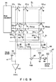
- Fig. 9 shows a PROM according to a second embodiment of the invention.
- this PROM has memory-cell matrix 31.
- Matrix 31 comprises floating gate, and n-channel MOS transistors 32 ll to 32 mn , used as memory cells and arranged in rows and columns. The control gates of the MOS transistors forming each row are coupled to a row-signal line.
- MOS transistors 32 ll to 32 ln of the first row have their control gates coupled to the first row-signal line 33 l
- MOS transistors 32 2l to 32 2n of the second row have their control gates coupled to the second row-signal line 332, and so forth.
- MOS transistors 32 ml to 32 mn of the last row have their control gates connected to the last row-signal line 33 m .
- the drains of the MOS transistors forming each column are coupled to a column-signal line.
- MOS transistors 32 ll to 32 ml of the first column have their drains connected to the first column-signal line 34 l
- MOS transistors 32 l2 to 32 m2 of the second column have their drains coupled to the second column-signal line 342, and so forth.
- MOS transistors 32 ln to 32 mn of the last column have their drains connected to the last column-signal line 34 n .
- the sources of n-channel MOS transistors 32 ll to 32 mn are connected to the ground.
- the PROM further comprises row decoder 35 and column-selecting circuits 61 and 62.
- First column-selecting circuit 61 is used to read data from memory-cell matrix 31, and second column-selecting circuit 62 is used to write data in memory-cell matrix 31.
- First column-selecting circuit 61 comprises column-selecting MOS transistors 63 l to 63 n .
- MOS transistors 63 l to 63 n are n-channel transistors and are turned on by output address signals A l to A n of a column decoder (not shown) which is used to read data from memory-cell matrix 31.
- MOS transistors 63 l to 63 n are connected at one end to column-signal lines 34 l to 34 n , respectively. They are connected at the other end to each other.
- Second column-selecting circuit 62 comprises column-selecting MOS transistors 64 l to 64 n .
- MOS transistors 64 l to 64 n are p-channel transistors and are turned on by output address signals B l ⁇ to B n ⁇ of another column decoder (not shown), which is provided to write data in memory-cell matrix 31.
- MOS transistors 64 l to 64 n are connected at one end to column-signal lines 34 l to 34 n , respectively, and are connected to each other at the other end.
- the node of the other ends of MOS transistors 63 l to 63 n is connected to one end of data-reading, n-channel MOS transistor 38.
- the node of the other ends of MOS transistors 64 l to 64 n is coupled to one end of data-writing, p-channel MOS transistor 65.
- the other end of data-reading MOS transistor 38 is coupled to the input terminal of sense amplifier circuit 40 and also to resistor 42 which in turn is coupled to power supply Vcc.
- Transistor 38 is turned on by a read-mode signal.
- the other end of data-writing MOS transistor 65 is coupled to high-voltage power supply Vpp.
- Transistor 65 is turned on by the output signal of buffer circuit 43 which is coupled to power supply Vpp.
- buffer circuit 43 The input terminal of buffer circuit 43 is connected to the output terminal of NAND gate 66 for providing the logical sum of the write-mode signal and data Din to be written into the PROM.
- Buffer circuit 43 and NAND gate 66 constitute gate circuit 67 for writing data into the PROM.
- the read-mode signal at level "1" is supplied to data-reading MOS transistor 38, and the write-mode signal at level "0" is supplied to one of the two input terminals of NAND gate 66.
- MOS transistor 38 is turned on, and data-writing MOS transistor 65 is turned off.
- the write-mode signal at level "1" is supplied to the first input terminal of NAND gate 66, and the read-mode signal at level "0" is supplied to data-reading MOS transistor 38. All outputs of the data-reading, column decoder are set at level "0". Therefore, MOS transistor 38 and all MOS transistors 63 l to 63 n of first column-selecting circuit 61 are turned off. When data Din is "1" in this condition, the output of NAND gate 66 falls to level "0", whereby data-writing MOS transistor 65 is turned on.
- a high voltage is thereby applied from high-voltage power source Vpp to column-signal line 34 j through MOS transistor 65 and then through column-selecting MOS transistor 64 j selected by the data-writing, column decoder.
- Data "0" is thus written into memory cell 32 ij connected to row-signal line 33 i selected by row decoder 35 and to column-signal line 34 j selected by the data-writing, column decoder.
- the output of NAND gate 66 rises to level "1". In this case, data-writing MOS transistor 65 is turned off.
- Fig. 10 shows memory cell 32 ij and the circuit for writing data into this cell 32 ij .
- a voltage at GND level i.e., level "0” is applied to the gate of data-writing MOS transistor 65, and also to the gate of column-selecting MOS transistor 64 j used for writing data.
- High voltage Vpp is applied to the back gates of MOS transistors 65 and 64 j .
- Both transistors 65 and 64j are of p-channel type, and their drain potentials Vc and Vd are not lowered by the threshold voltage and are thus equal to voltage Vpp applied to the source of transistor 65.
- high voltage Vpp is applied between the source and drain of memory cell 32 ij , whereby a current great enough to write data "0" into cell 32 ij is obtained.
- first column-selecting circuit 61 comprising n-channel MOS transistors 63 l to 63 n for reading data from memory cells 32 ll to 32 mn
- second column-selecting circuit 62 comprising p-channel MOS transistors 64 l to 64 n for writing data into memory cells 32 ll to 32 mn
- Second column-selecting circuit 62 is used to apply voltage Vpp to the drains of memory cells 32 ll to 32 mn .
- First column-selecting circuit 61 is used to read GND-level or level "0" data since the sources of memory cells 32 ll to 32 mn , which are n-channel transistors, are at GND potential.
- MOS transistors 63 l to 63 n of first column-selecting circuit 61 must be of n-channel type in order to read GND-level data. Were they p-channel MOS transistors, their drain potential would not be at the GND level. Rather, their drain potential would be at a level higher than the GND level by V THP , i.e., the threshold voltage of the p-channel MOS transistors.
- Vpp Since two column-selecting circuits 61 and 62 are used, high voltage Vpp does not fall when data "0" is written into any memory cell. Hence, not only data “1” but also data “0” can be efficiently written into the memory cells, even if voltage Vpp is set at a relatively low level. Therefore, voltage Vpp is set at a low level, thus preventing a deterioration of the LSI in which the PROM is incorporated, and also preventing a latch-up phenomenon. For the same reason, the Vpp-generating circuit can be fabricated within the LSI, involving no particular technical difficulties.
- Fig. 11 shows a further PROM, according to a third embodiment of the present invention.
- the same numerals and symbols are used to denote the same elements as used in the PROM shown in Fig. 9.
- This PROM differs from the PROM of Fig. 9 in that one column-selecting circuit 71 is used in place of two circuits 61 and 62.
- This column-selecting circuit 71 comprises complementary transmission gates 70 l to 70 n , each consisting of one n-channel MOS transistors and one p-channel MOS transistor. More specifically, as is shown in Fig.
- first gate 70 l consists of n-channel MOS transistor 68 l and p-channel MOS transistor 69 l
- second gate 702 consists of n-channel MOS transistors 682 and p-channel MOS transistor 692, and so forth.
- last gate 70 n consists of n-channel MOS transistor 68 n and p-channel MOS transistor 69 n .
- the n-channel and p-channel MOS transistors are connected in parallel to each other.
- the n-channel MOS transistors 68 l to 68 n of transmission gates 70 l to 70 n are turned on by decode signals A l to A n output from a column decoder (not shown), thereby to read data from memory cells 32 ll to 32 mn .
- the p-channel MOS transistors 69 l to 69 n of transmission gates 70 l to 70 n are turned on by decode signals A l to A n output from the decoder (not shown) whose level is inverted to that of signals A l to A n , thereby to write data into memory cells 32 ll to 32 mn .
- the transmission gates can function in both a data-read mode and a data-write mode, in accordance with decode signals A l to A n output from the column decoder (not shown) and decode signals A1 to An obtained by inverting decode signals A l to A n .
- the GND-level data is output through the n-channel MOS transistor of a transmission gate, and the Vpp-level data is input through the p-channel MOS transistor of the transmission gate. Therefore, high voltage Vpp does not fall by the threshold voltage V THN of the n-channel MOS transistor when data "0" is written into the selected memory cell. Neither does the GND-level voltage rise by the threshold voltage V THP of the p-channel MOS transistor when data "0" is read from the selected memory cell.
- the PROM of Fig. 11 has only one column-selecting circuit, i.e., circuit 71. It follows that this PROM needs to have only one column decoder. Decode signals A l to A n , and A1 to A n are used to control transmission gates 70 l to 70 n . Hence, the PROM of Fig. 11 does not require so large a pattern area as the PROM shown in Fig. 9.
- Fig. 12 illustrates still another PROM, according to a fourth embodiment of the present invention.
- the same numerals and symbols are used to represent the same elements as used in the PROM shown in Fig. 9.
- This PROM differs from that of Fig. 9 in that first column-selecting circuit 61 for reading data is provided on one side of memory-cell array 31, whereas second column-selecting circuit 62 for writing data is provided on the other side of array 31.
- This specific arrangement reduces the required area on the semiconductor chip.
- Column-signal lines 34 l to 34 n are arranged parallel at extremely short intervals, thereby raising the integration density of the PROM.
- column-selecting circuits 61 and 62 ensures complete electrical isolation between n-channel MOS transistors 63 l to 63 n , on the one hand, and p-channel MOS transistors 64 l to 64 n , on the other. That is, if n-channel MOS transistors 63 l to 63 n were arranged near p-channel MOS transistors 64 l to 64 n as in the PROM shown in Fig. 9, a latch-up phenomenon would likely occur. This undesired phenomenon should be avoided at all cost, because, in writing data in the PROM, a large current of tens of milliamperes flows through data-writing MOS transistors 64 l to 64 n .
- Fig. 13 shows the pattern in which the elements of column-selecting circuit 62 for writing data are arranged in the PROM illustrated in Fig. 12.
- the same numerals and symbols are used to designate the same elements as shown in Fig. 12.
- aluminum strips 81 l to 81 l5 are arranged parallel to one another.
- Contacts holes 82 l to 82 l8 are provided to connect some elements to others.
- Polycrystalline silicon layers 83 l to 837 and diffusion layers 84 l and 842 are also provided.
- Numerals 85 l to 854 denote the floating gates of memory cells 32 l to 324.
- MOS transistors 64 l to 644 are formed in the hatched regions.
- the present invention can provide a semiconductor memory wherein, even if the memory cells have different operation points arising from differences in their respective process parameters, the data-writing characteristic of each memory cell can be sufficiently stable, thereby ensuring that data can be written into each cell at high speed, and which can, therefore, be manufactured with a high yield.
- the present invention can provide a semiconductor memory wherein data "0" can be written into each memory cell at a sufficiently high speed, even if the data-writing voltage is relatively low.
Landscapes
- Engineering & Computer Science (AREA)
- Microelectronics & Electronic Packaging (AREA)
- Read Only Memory (AREA)
Claims (5)
- Halbleiterspeicher, umfassen:
Einrichtungen zum Anschließen eines Datenschreibpotentials;
Einrichtungen zum Anschließen eines Bezugspotentials;
eine PROM-Zelle (21), einen ersten MOS-Transistor (51) und einen zweiten MOS-Transistor (52), die in Reihe zwischen das Datenschreibpotential und das Bezugspotential geschaltet sind, wobei
die PROM-Zelle (21) einem ersten Kanaltyp angehört und elektrisch zur Speicherung von Daten programmierbar ist; und
der erste MOS-Transistor (51) einem zweiten Kanaltyp angehört;
dadurch gekennzeichnet,
daß ein Gate der PROM-Zelle ein Zeilenwählsignal empfängt;
ein Gate des ersten MOS-Transistors (51) ein Schreibsignal zur Bestimmung des Arbeitspunktes der PROM-Zelle empfängt, wenn der Speicher in einen Datenschreibmodus gesetzt ist; und
der zweite MOS-Transistor (52) einem zweiten Kanaltyp angehört und ein Gate des zweiten MOS-Transistors ein Spaltenwählsignal zur Verringerung der für das Einschreiben von Daten in die PROM-Zelle erforderlichen Zeit empfängt; und weiter aufweisend:
Einrichtungen zur Erzeugung und Lieferung des Zeilenwählsignals an das Gate der PROM-Zelle;
Einrichtungen zur Erzeugung und Lieferung des Schreibsignals an das Gate des ersten MOS-Transistors; und
Einrichtungen zur Erzeugung und Lieferung des Spaltenwählsignals an das Gate des zweiten MOS-Transistors. - Halbleiterspeicher nach Anspruch 1, dadurch gekennzeichnet, daß die PROM-Zelle ein n-Kanal-MOS-Transistor ist und der erste und der zweite MOS-Transistor (51, 52) jeweils p-Kanal-Transistoren sind.
- Halbleiterspeicher nach Anspruch 1, dadurch gekennzeichnet, daß die PROM-Zelle (21) ein MOS-Transistor mit schwebendem Gate ist.
- Halbleiterspeicher, umfassend:
eine Vielzahl von n-Kanal-MOS-Transistoren mit schwebendem Gate, die in Zeilen und Spalten angeordnet sind und als Speicherzellen (32ll bis 32mn) benutzt werden;
eine Vielzahl von Zeilenleitungen (33l bis 33m), die zahlenmäßig den Zeilen der Speicherzellen entsprechen, wobei eine einzelne Zeilenleitung jeweils an das Gate jedes der Speicherzellen der entsprechenden Reihe angeschlossen ist;
eine Vielzahl von Spaltenleitungen (34l bis 34n), die zahlenmäßig den Spalten der Speicherzellen entsprechen, wobei eine einzelne Spaltenleitung jeweils an den Drain jeder der Speicherzellen der entsprechenden Spalte angeschlossen ist;
eine datenschreibende, spaltenwählende Schaltung (62, 71) mit einer Vielzahl von p-Kanal-MOS-Transistoren (64l bis 64n), von denen jede mit einem Ende jeweils an eine der Spaltenleitungen angeschlossen ist und durch Datenschreib-, Spaltendekodiersignale gesteuert wird;
eine datenlesende, spaltenwählende Schaltung (61, 71) mit einer Vielzahl von n-Kanal-MOS-Transistoren (63l bis 63n; 68l bis 68n), von denen jeder mit einem Ende jeweils an eine der Spaltenleitungen angeschlossen ist und von datenlesenden, spaltendekodierenden Signalen gesteuert wird;
dadurch gekennzeichnet, daß
ein datenschreibender p-Kanal-MOS-Transistor (65) an die anderen Enden der p-Kanal-MOS-Transistoren der datenschreibenden, spaltenwählenden Schaltung angeschlossen ist, um eine hohe Spannung an diejenigen Speicherzellen zu legen, die gewählt und eingeschaltet werden, wenn der Halbleiterspeicher in den Datenschreibmodus mit Pegel "0" gesetzt ist; und
daß die p-Kanal-MOS-Transistoren (69l bis 69n) der datenschreibenden, spaltenwählenden Schaltung den n-Kanal-MOS-Transistoren (68l bis 68n) jeweils der datenschreibenden, spaltenwählenden Schaltung parallelgeschaltet sind, wodurch Durchlaßtore (17l bis 17n) geschaffen werden. - Halbleiterspeicher, umfassend:
eine Vielzahl von n-Kanal-MOS-Transistoren mit schwebendem Gate, die in Zeilen und Spalten angeordnet sind und als Speicherzellen (32ll bis 32mn) benutzt werden;
eine Vielzahl von Zeilenleitungen (33l bis 33m), die zahlenmäßig den Zeilen der Speicherzellen entsprechen, wobei eine Zeilenleitung an das Gate jedes der Speicherzellen der entsprechenden Reihe angeschlossen ist;
eine Vielzahl von Spaltenleitungen (34l bis 34n), die zahlenmäßig den Spalten der Speicherzellen entsprechen, wobei eine Spaltenleitung an den Drain jeder der Speicherzellen der entsprechenden Spalte angeschlossen ist;
eine datenschreibende, spaltenwählende Schaltung (62, 71) mit einer Vielzahl von p-Kanal-MOS-Transistoren (64l bis 64n), von denen jede mit einem Ende jeweils an eine der Spaltenleitungen angeschlossen ist und durch Datenschreib-, Spaltendekodiersignale gesteuert wird;
eine datenlesende, spaltenwählende Schaltung (61, 71) mit einer Vielzahl von n-Kanal-MOS-Transistoren (63l bis 63n; 68l bis 68n), von denen jeder mit einem Ende jeweils an eine der Spaltenleitungen angeschlossen ist und von Datenlese-, Spaltendekodiersignalen gesteuert wird;
dadurch gekennzeichnet, daß
ein datenschreibender p-Kanal-MOS-Transistor (65) an die anderen Enden der p-Kanal-MOS-Transistoren der datenschreibenden, spaltenwählenden Schaltung angeschlossen ist, um eine hohe Spannung an diejenigen Speicherzellen zu legen, die gewählt und eingeschaltet werden, wenn der Halbleiterspeicher in den Datenschreibmodus mit Pegel "0" gesetzt ist; und
wobei die datenschreibende, spaltenwählende Schaltung (62, 71) und die Datenlese-, Spaltenwählschaltung (61, 71) an entgegengesetzten Seiten einer Zellenmatrix angeordnet sind, die die MOS-Transistoren mit schwebendem Gate umfaßt.
Applications Claiming Priority (4)
| Application Number | Priority Date | Filing Date | Title |
|---|---|---|---|
| JP61231721A JPS6386195A (ja) | 1986-09-30 | 1986-09-30 | 半導体記憶装置 |
| JP231721/86 | 1986-09-30 | ||
| JP61231803A JPS6386196A (ja) | 1986-09-30 | 1986-09-30 | 半導体記憶装置 |
| JP231803/86 | 1986-09-30 |
Publications (3)
| Publication Number | Publication Date |
|---|---|
| EP0263318A2 EP0263318A2 (de) | 1988-04-13 |
| EP0263318A3 EP0263318A3 (en) | 1990-12-12 |
| EP0263318B1 true EP0263318B1 (de) | 1993-02-24 |
Family
ID=26530050
Family Applications (1)
| Application Number | Title | Priority Date | Filing Date |
|---|---|---|---|
| EP87113251A Expired - Lifetime EP0263318B1 (de) | 1986-09-30 | 1987-09-10 | Halbleiterspeicher |
Country Status (3)
| Country | Link |
|---|---|
| US (2) | US5050124A (de) |
| EP (1) | EP0263318B1 (de) |
| DE (1) | DE3784298T2 (de) |
Families Citing this family (7)
| Publication number | Priority date | Publication date | Assignee | Title |
|---|---|---|---|---|
| US5175704A (en) * | 1987-07-29 | 1992-12-29 | Kabushiki Kaisha Toshiba | Nonvolatile semiconductor memory device |
| KR910007434B1 (ko) * | 1988-12-15 | 1991-09-26 | 삼성전자 주식회사 | 전기적으로 소거 및 프로그램 가능한 반도체 메모리장치 및 그 소거 및 프로그램 방법 |
| EP0926686A1 (de) * | 1997-12-23 | 1999-06-30 | STMicroelectronics S.r.l. | Nichtflüchtiger Seriell-Flash-, EPROM-, EEPROM-, und Flash-EEPROM-Speicher in AMG-Konfiguration |
| JP4663094B2 (ja) | 2000-10-13 | 2011-03-30 | 株式会社半導体エネルギー研究所 | 半導体装置 |
| JP2006164447A (ja) * | 2004-12-09 | 2006-06-22 | Toshiba Corp | 半導体記憶装置 |
| ITTO20080647A1 (it) * | 2008-08-29 | 2010-02-28 | St Microelectronics Srl | Decodificatore di colonna per dispositivi di memoria non volatili, in particolare del tipo a cambiamento di fase |
| US9007822B2 (en) * | 2012-09-14 | 2015-04-14 | Micron Technology, Inc. | Complementary decoding for non-volatile memory |
Family Cites Families (11)
| Publication number | Priority date | Publication date | Assignee | Title |
|---|---|---|---|---|
| US4387444A (en) * | 1980-07-07 | 1983-06-07 | Hughes Aircraft Company | Non-volatile semiconductor memory cells |
| EP0050005B1 (de) * | 1980-10-15 | 1988-05-18 | Kabushiki Kaisha Toshiba | Halbleiterspeicher mit Programmierungszeit |
| JPS59218696A (ja) * | 1983-05-26 | 1984-12-08 | Toshiba Corp | 半導体メモリ |
| JPS6025269A (ja) * | 1983-07-21 | 1985-02-08 | Hitachi Ltd | 半導体記憶素子 |
| GB2160046B (en) * | 1984-04-20 | 1987-12-23 | Hitachi Ltd | Semiconductor memory device |
| JPS6197976A (ja) * | 1984-10-19 | 1986-05-16 | Hitachi Ltd | 半導体集積回路装置 |
| JPS61151898A (ja) * | 1984-12-26 | 1986-07-10 | Fujitsu Ltd | 半導体記憶装置におけるワ−ド線ドライバ回路 |
| JPH0746515B2 (ja) * | 1984-12-28 | 1995-05-17 | 日本電気株式会社 | デコ−ダ回路 |
| US4761764A (en) * | 1985-04-18 | 1988-08-02 | Nec Corporation | Programmable read only memory operable with reduced programming power consumption |
| US4663740A (en) * | 1985-07-01 | 1987-05-05 | Silicon Macrosystems Incorporated | High speed eprom cell and array |
| US4829203A (en) * | 1988-04-20 | 1989-05-09 | Texas Instruments Incorporated | Integrated programmable bit circuit with minimal power requirement |
-
1987
- 1987-09-09 US US07/094,706 patent/US5050124A/en not_active Expired - Lifetime
- 1987-09-10 DE DE8787113251T patent/DE3784298T2/de not_active Expired - Fee Related
- 1987-09-10 EP EP87113251A patent/EP0263318B1/de not_active Expired - Lifetime
-
1989
- 1989-12-07 US US07/447,391 patent/US4954991A/en not_active Expired - Lifetime
Also Published As
| Publication number | Publication date |
|---|---|
| DE3784298D1 (de) | 1993-04-01 |
| EP0263318A2 (de) | 1988-04-13 |
| EP0263318A3 (en) | 1990-12-12 |
| US4954991A (en) | 1990-09-04 |
| DE3784298T2 (de) | 1993-07-22 |
| US5050124A (en) | 1991-09-17 |
Similar Documents
| Publication | Publication Date | Title |
|---|---|---|
| US6674667B2 (en) | Programmable fuse and antifuse and method therefor | |
| US4103189A (en) | Mos buffer circuit | |
| US6521958B1 (en) | MOSFET technology for programmable address decode and correction | |
| US5515319A (en) | Non-volatile memory cell and level shifter | |
| US5557569A (en) | Low voltage flash EEPROM C-cell using fowler-nordheim tunneling | |
| KR100193101B1 (ko) | 비휘발성 반도체 기억장치 및 그 구동방법 | |
| EP0880144B1 (de) | Festwertspeicher | |
| US4761765A (en) | Semiconductor memory device having improved data output circuit | |
| JP3197168B2 (ja) | 半導体記憶装置の駆動方法 | |
| EP0337433B1 (de) | Zellenmusteranordnung einer Halbleiterspeichereinrichtung | |
| KR100712087B1 (ko) | 반도체메모리장치및그제조방법 | |
| US5469397A (en) | Semiconductor memory device with a reference potential generator | |
| KR100346991B1 (ko) | 반도체 기억 장치 | |
| US5580809A (en) | Method of making a mask ROM using tunnel current detection to store data | |
| US5966324A (en) | Static semiconductor memory device driving bit line potential by bipolar transistor shared by adjacent memory cells | |
| US4845538A (en) | E2 prom cell including isolated control diffusion | |
| EP0263318B1 (de) | Halbleiterspeicher | |
| EP0376290B1 (de) | Nichtflüchtige Halbleiterspeicheranordnung, fähig um einen durch einen Überlöschungszustand verursachten Lesefehler zu verhindern | |
| US6829179B2 (en) | Semiconductor storage device having substrate potential control | |
| US5502669A (en) | Electrically erasable and programmable read only memory device having selectively erasable sectors | |
| JP3084582B2 (ja) | 半導体記憶装置 | |
| JP2001028193A (ja) | 半導体記憶装置 | |
| JPH08236650A (ja) | 不揮発性半導体記憶装置及びその書き込み方法 | |
| JPH02356A (ja) | 半導体装置 | |
| JPH05283610A (ja) | 半導体記憶装置 |
Legal Events
| Date | Code | Title | Description |
|---|---|---|---|
| PUAI | Public reference made under article 153(3) epc to a published international application that has entered the european phase |
Free format text: ORIGINAL CODE: 0009012 |
|
| 17P | Request for examination filed |
Effective date: 19870910 |
|
| AK | Designated contracting states |
Kind code of ref document: A2 Designated state(s): DE FR GB |
|
| PUAL | Search report despatched |
Free format text: ORIGINAL CODE: 0009013 |
|
| AK | Designated contracting states |
Kind code of ref document: A3 Designated state(s): DE FR GB |
|
| 17Q | First examination report despatched |
Effective date: 19910626 |
|
| GRAA | (expected) grant |
Free format text: ORIGINAL CODE: 0009210 |
|
| AK | Designated contracting states |
Kind code of ref document: B1 Designated state(s): DE FR GB |
|
| REF | Corresponds to: |
Ref document number: 3784298 Country of ref document: DE Date of ref document: 19930401 |
|
| ET | Fr: translation filed | ||
| PLBE | No opposition filed within time limit |
Free format text: ORIGINAL CODE: 0009261 |
|
| STAA | Information on the status of an ep patent application or granted ep patent |
Free format text: STATUS: NO OPPOSITION FILED WITHIN TIME LIMIT |
|
| 26N | No opposition filed | ||
| PGFP | Annual fee paid to national office [announced via postgrant information from national office to epo] |
Ref country code: FR Payment date: 19970909 Year of fee payment: 11 |
|
| PGFP | Annual fee paid to national office [announced via postgrant information from national office to epo] |
Ref country code: DE Payment date: 19970919 Year of fee payment: 11 |
|
| REG | Reference to a national code |
Ref country code: GB Ref legal event code: 746 Effective date: 19981103 |
|
| PG25 | Lapsed in a contracting state [announced via postgrant information from national office to epo] |
Ref country code: FR Free format text: LAPSE BECAUSE OF NON-PAYMENT OF DUE FEES Effective date: 19990531 |
|
| PG25 | Lapsed in a contracting state [announced via postgrant information from national office to epo] |
Ref country code: DE Free format text: LAPSE BECAUSE OF NON-PAYMENT OF DUE FEES Effective date: 19990701 |
|
| REG | Reference to a national code |
Ref country code: FR Ref legal event code: ST |
|
| REG | Reference to a national code |
Ref country code: GB Ref legal event code: IF02 |
|
| PGFP | Annual fee paid to national office [announced via postgrant information from national office to epo] |
Ref country code: GB Payment date: 20060906 Year of fee payment: 20 |
|
| REG | Reference to a national code |
Ref country code: GB Ref legal event code: PE20 |
|
| PG25 | Lapsed in a contracting state [announced via postgrant information from national office to epo] |
Ref country code: GB Free format text: LAPSE BECAUSE OF EXPIRATION OF PROTECTION Effective date: 20070909 |