EP0098932A2 - Système à multi-niveaux réparable pour dispositif semi-conducteur - Google Patents
Système à multi-niveaux réparable pour dispositif semi-conducteur Download PDFInfo
- Publication number
- EP0098932A2 EP0098932A2 EP83104479A EP83104479A EP0098932A2 EP 0098932 A2 EP0098932 A2 EP 0098932A2 EP 83104479 A EP83104479 A EP 83104479A EP 83104479 A EP83104479 A EP 83104479A EP 0098932 A2 EP0098932 A2 EP 0098932A2
- Authority
- EP
- European Patent Office
- Prior art keywords
- wiring
- contacts
- chip
- planar support
- support frame
- Prior art date
- Legal status (The legal status is an assumption and is not a legal conclusion. Google has not performed a legal analysis and makes no representation as to the accuracy of the status listed.)
- Granted
Links
Images


Classifications
-
- H—ELECTRICITY
- H10—SEMICONDUCTOR DEVICES; ELECTRIC SOLID-STATE DEVICES NOT OTHERWISE PROVIDED FOR
- H10W—GENERIC PACKAGES, INTERCONNECTIONS, CONNECTORS OR OTHER CONSTRUCTIONAL DETAILS OF DEVICES COVERED BY CLASS H10
- H10W70/00—Package substrates; Interposers; Redistribution layers [RDL]
- H10W70/60—Insulating or insulated package substrates; Interposers; Redistribution layers
- H10W70/611—Insulating or insulated package substrates; Interposers; Redistribution layers for connecting multiple chips together
-
- H—ELECTRICITY
- H10—SEMICONDUCTOR DEVICES; ELECTRIC SOLID-STATE DEVICES NOT OTHERWISE PROVIDED FOR
- H10W—GENERIC PACKAGES, INTERCONNECTIONS, CONNECTORS OR OTHER CONSTRUCTIONAL DETAILS OF DEVICES COVERED BY CLASS H10
- H10W40/00—Arrangements for thermal protection or thermal control
- H10W40/60—Securing means for detachable heating or cooling arrangements, e.g. clamps
- H10W40/611—Bolts or screws
-
- H—ELECTRICITY
- H10—SEMICONDUCTOR DEVICES; ELECTRIC SOLID-STATE DEVICES NOT OTHERWISE PROVIDED FOR
- H10W—GENERIC PACKAGES, INTERCONNECTIONS, CONNECTORS OR OTHER CONSTRUCTIONAL DETAILS OF DEVICES COVERED BY CLASS H10
- H10W70/00—Package substrates; Interposers; Redistribution layers [RDL]
- H10W70/60—Insulating or insulated package substrates; Interposers; Redistribution layers
- H10W70/62—Insulating or insulated package substrates; Interposers; Redistribution layers characterised by their interconnections
- H10W70/641—Adaptable interconnections, e.g. fuses or antifuses
-
- H—ELECTRICITY
- H10—SEMICONDUCTOR DEVICES; ELECTRIC SOLID-STATE DEVICES NOT OTHERWISE PROVIDED FOR
- H10W—GENERIC PACKAGES, INTERCONNECTIONS, CONNECTORS OR OTHER CONSTRUCTIONAL DETAILS OF DEVICES COVERED BY CLASS H10
- H10W90/00—Package configurations
- H10W90/401—Package configurations characterised by multiple insulating or insulated package substrates, interposers or RDLs
-
- H—ELECTRICITY
- H10—SEMICONDUCTOR DEVICES; ELECTRIC SOLID-STATE DEVICES NOT OTHERWISE PROVIDED FOR
- H10W—GENERIC PACKAGES, INTERCONNECTIONS, CONNECTORS OR OTHER CONSTRUCTIONAL DETAILS OF DEVICES COVERED BY CLASS H10
- H10W40/00—Arrangements for thermal protection or thermal control
- H10W40/20—Arrangements for cooling
- H10W40/231—Arrangements for cooling characterised by their places of attachment or cooling paths
-
- H—ELECTRICITY
- H10—SEMICONDUCTOR DEVICES; ELECTRIC SOLID-STATE DEVICES NOT OTHERWISE PROVIDED FOR
- H10W—GENERIC PACKAGES, INTERCONNECTIONS, CONNECTORS OR OTHER CONSTRUCTIONAL DETAILS OF DEVICES COVERED BY CLASS H10
- H10W40/00—Arrangements for thermal protection or thermal control
- H10W40/20—Arrangements for cooling
- H10W40/231—Arrangements for cooling characterised by their places of attachment or cooling paths
- H10W40/235—Arrangements for cooling characterised by their places of attachment or cooling paths attached to package parts
-
- H—ELECTRICITY
- H10—SEMICONDUCTOR DEVICES; ELECTRIC SOLID-STATE DEVICES NOT OTHERWISE PROVIDED FOR
- H10W—GENERIC PACKAGES, INTERCONNECTIONS, CONNECTORS OR OTHER CONSTRUCTIONAL DETAILS OF DEVICES COVERED BY CLASS H10
- H10W40/00—Arrangements for thermal protection or thermal control
- H10W40/60—Securing means for detachable heating or cooling arrangements, e.g. clamps
- H10W40/625—Clamping parts not primarily conducting heat
-
- H—ELECTRICITY
- H10—SEMICONDUCTOR DEVICES; ELECTRIC SOLID-STATE DEVICES NOT OTHERWISE PROVIDED FOR
- H10W—GENERIC PACKAGES, INTERCONNECTIONS, CONNECTORS OR OTHER CONSTRUCTIONAL DETAILS OF DEVICES COVERED BY CLASS H10
- H10W72/00—Interconnections or connectors in packages
- H10W72/071—Connecting or disconnecting
- H10W72/072—Connecting or disconnecting of bump connectors
- H10W72/07251—Connecting or disconnecting of bump connectors characterised by changes in properties of the bump connectors during connecting
-
- H—ELECTRICITY
- H10—SEMICONDUCTOR DEVICES; ELECTRIC SOLID-STATE DEVICES NOT OTHERWISE PROVIDED FOR
- H10W—GENERIC PACKAGES, INTERCONNECTIONS, CONNECTORS OR OTHER CONSTRUCTIONAL DETAILS OF DEVICES COVERED BY CLASS H10
- H10W72/00—Interconnections or connectors in packages
- H10W72/20—Bump connectors, e.g. solder bumps or copper pillars; Dummy bumps; Thermal bumps
Definitions
- This invention relates to integrated circuit semiconductor chips and, in particular, to the repair of defective interconnection lines, semiconductor dies and/ or subassemblies and improvement of the engineering design of the packaging device. Specifically, the invention relates to a repairable multi-level overlay wiring system for a multi-level integrated packaging structure.
- a variety of packaging structures for mounting integrated circuit chips on substrates are known in the art.
- One common technique utilizes mounting of integrated circuit chips onto substrates which carry film or printed circuits.
- the integrated circuit chip is mounted face upward, with the array of connection contact areas uppermost such that connection between the contact areas and the jumper lands on the substrate is made by thin jumper wires extending over the edges of the chip.
- This technique is shown in U.S. Patent 3 082 327.
- the converse situation is also employed where the chip is mounted face downward and its contact areas are bonded to conductor lands on the substrate. This is shown in U.S. Patent 3 292 240.
- Multi-level overlay wiring systems are also used for mounting semiconductor chips. These systems employ a plurality of layers for power distribution, a plurality of layers for chip-to-chip connections, and a plurality of layers for intrachip connections.
- a composite package comprising a number of discrete wiring layers is generally known as a multi-layer ceramic (MLC).
- MLC multi-layer ceramic
- Defects in the conductors in some of the layers are generally repaired by means of so-called engineering changes in the semiconductor packages.
- These engineering changes (EC) have, in the past, employed complex techniques to make connections involving the use of discrete wires on various surfaces of the ceramic from an EC pad to the conductor in question. Such changes have been made by the use of fly wires which in practice are difficult to use given the dimensional constraints of the system. In extreme situations the MLC is unrepairable since the defect may not be circumvented.
- fly wires As VLSI circuit dimensions tend to decrease with increased packing density, the removal of insulation from the ends of fly wires becomes an inefficient technique in terms of fabrication labor costs and the propensity of operator error tending to damage or render useless the MLC. Moreover, the technique is labor intensive requiring discrete soldering from point to point as the EC is made. Hence, the use of fly wires is not cost effective.
- the chip itself includes a solid state device having a plurality of separate or structural integrated resistors, diodes, resistors and capacitors formed in the monolithic body of the semiconductor material which must be protected during the joining operation.
- the integrated circuit cannot readily be isolated from the conductor for couplings forming the I/O to the chip.
- Various packaging structures have been proposed in the prior art to provide the necessary cooling, thermal and mechanical shock resistance to this integrated circuit while at the same time providing sufficient reliability of any conductor coupling.
- U.S. Patent 3 325 882 relates to a method of interconnecting metal lands located on an insulating substrate to selected metal lands located on the solid state device.
- the method perceives the use of a removable powdered material in a cavity space disposed about the solid state device. This permits a bridging metal interconnection to be made between the solid state device and the substrate.
- U.S. Patent 3 614 832 A different technique is shown in U.S. Patent 3 614 832.
- a decal including a backing plate with a plurality of conductive strips which can be adhered to the plate by means of a soluble adhesive.
- the decal is positioned over a substrate to which the solid state device has been positioned with the strips in registration with respective contacts and lands.
- the strips are brought into contact with respective contact and land surface portions and then subjected to heat and pressure treatment so that bonding between the strips and land surface portions occurs.
- the decal backing plate may be removed from the strips, for example, by dissolving the adhesive thereby leaving the strips firmly bonded to the contacts and lands bridging the space therebetween.
- U.S. Patent 3 605 063 relates to a system for interconnecting electrical components although not of VLSI size.
- printed circuit cards are used having individual electrical components mounted on the edge with electrical interconnection between the cards achieved using wiring cards of a specific design sandwiched between the component cards.
- Each of the component and wiring cards have on one side a plurality of paired and electrically connected conductive pads arranged in a matrix.
- One pad of each pair of pads is provided with a plated through hole to the other side of the card to a similar pad on that side.
- each pad pair is electrically isolated from the other pair and conductive paths connect the leads of the component to selected pad pairs.
- Different types of wiring cards are used to establish either vertical or horizontal conductive paths.
- U.S. Patent 3 662 230 relates to a interconnection system utilizing conductive patterns bonded to thin flexible insulating films.
- a packaging system as disclosed in that patent employs one or more semiconductor chips each having metal contact pads on at least one face.
- a rigid support is provided for the semiconductor chip and also large leads are used to connect the package device to an external circuit.
- Thin metallic film strips are bonded to a thin flexible dielectric sheet for support. The set of metal strips interconnects the contact paths of the semiconductor chips and selected leads to electrically interconnect the semiconductor device and the leads. If a plurality of semiconductor devices are used, a plurality of dielectric sheets are stacked with electrical connections made between the different layers of metal film strips through openings in the dielectric sheets.
- U.S. Patent 3 702 025 defines a system of interconnecting circuits on a substrate in a discretionary manner by first probing cells that are mounted on the substrate to determine which are defective or inoperative. The cells are covered by a dielectric layer, a second layer connection pattern is then formed and connections are made to contacts on only the good cells with the connection patterns skipping across defective cells.
- U.S. Patent 3 757 175 relates to a system of coplanar connections to semiconductor chips mounted on a single substrate by using a rigid dielectric substrate for supporting a number of semiconductor chips.
- the chips have metallized contact electrodes and an insulating material overlies one surface of the substrate in which the chips are embedded.
- the substrate has conductor strips with terminal electrodes to be used for connecting the contact electrodes.
- the chips are bonded to the substrate with the contact electrodes in registration with the terminal electrodes and with the contact and terminal electrodes contiguous with the surface of the insulating material.
- Metallization is then deposited on the surface of the insulating material extending between the contact and terminal electrodes to form electrical connections to the chips.
- U.S. Patent 3 780 352 also relates to a semiconductor interconnecting system utilizing conductive patterns bonded to thin flexible insulating films.
- a packaging system for a plurality of semiconductor chips each having metal contact pads on at least one face is disclosed.
- a rigid support is provided for the chips and also for a series of leads which are used to connect the package device to an external circuit.
- Thin metallic film strips are bonded to a thin flexible dielectric sheet for support.
- the metal strips in the form of sets then interconnect the contact pads on the semiconductor chips to selected leads and thereby establish electrical interconnections of the semiconductor device and the leads.
- a plurality of dielectric sheets can be stacked and interconnections then made between different layers of thin metal strips through openings in the dielectric sheets if couplings to a plurality of semiconductor devices are to be established.
- U.S. Patent 3 781 596 also deals with packaging of semiconductors by means of flexible carriers.
- the carrier comprises a film base having a pattern of discretionary conductors and bonding pads.
- the film acts as a supporting layer for the conductor pattern which itself is applied to one surface by selective deposition or etching of coatings in raised contact areas.
- the semiconductor chips are mounted so that the active chip surface is bonded to the carrier pads. Thereafter, the chip is connected to the circuitry of the substrate by the discretionary carrier conductor pattern.
- the carrier pads serve to provide discrete bonding areas for reliable bonding and prevent shorting by raising the carrier conductors of the active surface of the chip.
- U.S. Patent 3 978 578 relates to packaging of semiconductor devices utilizing a polyimide film with selected areas etched from the surface of the wafer. The etching exposes electrical contact areas of each of the semiconductor devices. The integrated circuit devices are then separated from the wafer and attached to a support. Electrical continuity is established by using bonding wires to couple the contact areas on each of the device with electrical conductors. The device is then coated with a second layer of polyimide film.
- U.S. Patent 4 072 982 discloses a semiconductor circuit having a plurality of plate-shaped semiconductor islands supported on a dielectric carrier. Doping layers are provided on the island and thin film deposits on selected areas of the dielectric carrier are used to interconnect selected islands.
- U.S. Patent 4 251 852 relates to a packaging structure for integrated circuits wherein a plurality of circuit chips are mounted on a number of membrane-like insulating members. Each of the membrane-like members provide multi-level wiring and interconnections between the chip or chips and a secondary wiring- structure.
- the insulating membrane is material such as polyimide or parylene and by photoresist and etching procedures a number of openings in the membrane are provided over an active area of a particular chip such that by subsequent masking and metal deposition steps, metallic lands are provided to form electrical paths between the openings over a chip and openings for a secondary structure contact grid.
- a second thin layer of membrane material is then provided over the metallization of the first layer and is similarly processed to provide an identical set of openings in the secondary grid structure for a second chip. Accordingly, the interconnection of two memory chips to a common set of contact openings with levels of metal lands insulated from each other is accomplished such that the contact openings in both levels conform to a predetermined format.
- U.S. Patent 4 254 445 relates to an EC repair of VLSI devices.
- An array of chips are mounted on a substrate such that about each chip area a large peripheral area is defined for EC pads and for testing.
- Prefabricated thin film interconnection EC lines of varying lengths are preformed in the rows and columns between the peripheral areas surrounding each of the chips.
- These printed wire EC lines and pads are designed to have different lengths and are laid out so that the EC pads for different chips can be interconnected at the discretion of the designer.
- the '445 patent perceives a general hierarchy of EC lines having a multi-tier of long vertical lines of parallel shorter lines, a series of horizontal lines and fly wire interconnections. This hierarchy uses a generally orthogonal structure such that fly wire connections are extremely short.
- Yet another object of this invention is to define a system of packaging integrated circuit chips so that successive joining of levels with the capability of engineering change exist between various levels of a multi-level wiring medium.
- a further object of this invention is to define a packaging system capable of handling a mix of integrated circuit configurations on a multi-chip carrier.
- the packaging structure utilizes a primary planar support frame having an array of support areas disposed in a geometric relationship.
- a wiring pattern is formed on the primary planar support frame to provide connection contacts and EC wiring channels and contacts within the space between the areas on the frame.
- a plurality of secondary planar support frames are positioned respectively within each of the areas. The configuration of each of the secondary planar support frames is slightly less than that of each of the areas forming the array on the primary planar support frame. Secondary areas are formed in each of the secondary planar support frames.
- An array of secondary areas of greater number than the primary areas are formed in a geometric pattern in each of the secondary planar support frames.
- Each of the secondary planar support frames contain a wiring pattern to provide connection contacts and engineering wiring channels and contacts in the space between each of the - areas on each of the planar support frames.
- each of the secondary areas a planar single chip carrier is disposed, each of the chip carriers containing at least one integrated circuit chip supported thereon and connected to that area.
- the chip carriers are respectively positioned within each of the secondary areas and have an array of exposed connection contacts.
- Each of the planar single chip carriers contain wiring for electrically interconnecting the integrated circuit chip supported thereon to the array of exposed connection contacts on the associated single chip carrier.
- a plurality of interconnection conductors are used for first connecting each of the single chip carriers to predetermined connection contacts on one of the secondary planar support frames.
- Secondary connectors are used for connecting specified predetermined contacts of each of the secondary planar support frames to predetermined connection contacts on the primary planar support frame. Accordingly, by this multiple, multi- level wiring technique, repair and'replacement of individual chip carriers with engineering wiring changes is greatly facilitated.
- each of the single chip carriers comprises an integrated circuit chip having an array of electrical contacts and a thin flexible membrane insulating member containing a wiring pattern.
- the wiring pattern of each of the membrane-like insulating members interconnects the array of electrical contacts of the membrane-like member and the array of electrical contacts of the integrated circuit chip positioned thereon.
- the present invention is directed to a repairable multi-level overlay wiring system for semiconductor chips.
- a thermal conduction module TCM
- This multi-level semiconductor device is exceptionally complicated and accordingly, by defining the invention in the context of that system, other configurations which are less complex will be apparent to those of working skill in this technology. Referring now to FIGS. 1 and 2, the basic concepts of this invention will be described.
- a semiconductor array is defined on a printed circuit board.
- the array employs an intermediate 9-chip carrier having a 3 x 3 matrix of single chip carriers.
- the 9-chip carrier is then itself arrayed in a 2 x 2 configuration on a 36-chip carrier.
- multi-level wiring repair capability is established by utilizing a repair wire system on the 9-chip carrier, a second repair wire capability on the 36-chip carrier and a third repair wire capability on the printed circuit board.
- the invention is not limited to a specific type of device carried by the 9-chip carrier.
- the invention as shown in FIG. 1A is applicable to a leadless carrier, or tape automated bond carrier or a mixture thereof. These particular types of carriers are well known in the art.
- a flip-chip can also be employed on the 9-chip carrier. Such devices are described in L.S. Goldman, "Geometric Optimization of Controlled Collapse Interconnections", IBM J. Res. & Dev., Vol. 13, No. 3, p. 251 et seq., May, 1969.
- FIG. 1A shows a mixture of these carrier types and it is within the scope of this invention to use either a mixture of carriers or a matrix or a single type.
- FIG. 2 illustrates a cross-section of a particular encapsulated single chip carrier shown in FIG. lA.
- a pair of contact wells (b), (c) are located on the outer perimeter of the wiring film.
- the contact wells are located with a fixed separation L 1 .
- Each signal circuit path from the semiconductor die is configured so that a pair of contact wells are serially disposed in the circuit path at that fixed separation.
- FIG. 2 shows the chip carrier as having a series of discrete levels, polyimide/metal denoted as levels P1-P3 and M1-M2.
- the circuit path in FIG. 2 is defined, that is, wired from the chip to a land (a) through metallization layer M 1 to the EC well (b) and then to the circuit well (c).
- Metallization in layer M 1 denoted as delete land (d) defines the circuit path from the EC-well (b) to the circuit well (c). It is understood that the semiconductor die may have a large number of signal, I/O paths and therefore the contact well pairs are equally distributed along the outer edges of the wiring film portion of the encapsulated chip structure.
- FIG. 1 shows the chip carrier as having a series of discrete levels, polyimide/metal denoted as levels P1-P3 and M1-M2.
- the circuit path in FIG. 2 is defined, that is, wired from the chip to a land (a) through metallization layer M 1 to the EC
- 1B broadly shows a series of via pairs which would be used to define the contact wells about the periphery of the encapsulated chip. While the pairs are shown along one side, it is understood that the via pairs would exist about the total periphery of the encapsulated chip.
- a cylindrical cooling stud (F) is fittingly attached over the integral metallic cap. Attachment of the cooling stud to the cap may be by reflow solder, epoxy bonding or pressure attachment with thermal grease to the surface of the cap. As is understood in this technology, an appropriate cooling stud support and positioning structure would be provided depending on the attachment technique to be employed.
- FIG. 2 also illustrates the multi-level wiring path.
- complementary attachment protrusions in the forms of hemispherical protrusions (G) are located on a wiring film layer (H).
- the protrusions (G) are separated by a distance (L) identical to that of the centerline distance between the contact wells.
- the hemispherical protrusions (G) may be formed by screening an appropriate volume of a suitable alloy on a pad of predetermined size.
- the metal of choice may be, for example, Pb/Sn alloy employed on the wiring film (H). Pad size and solder volume determine the height and shape of the protrusions.
- the contact well (c) has a diameter D 2 which is determined by the etching process employed at the polyimide level (P 3 ).
- the well diameter (D 2 ) must be less than the hemispherical protrusion diameter (D 1 ). Stated differently, D 1 > D 2 and the ratio of D 2 /D 1 ⁇ 1 will therefore result in a limited physical engagement so that the contact well (c) resting on the protrusion (G) at a chord (D 2 ) will effectuate a separation between layer P 3 and the wiring interface H.
- the separation is sufficient so that the reflow attached well (c) to the protrusion (G) will have a vertical distance to allow adequate solder flux clean- out.
- a bond film (J) is utilized to provide mechanical support for the encapsulated chip structure.
- the thickness of the film (J) is equal to that of the separation between the lower surface of P 3 and the wiring interface (H) thereby limiting moisture entrapment after processing for flux rinse and drying.
- the reflow attached well is screen filled with the solder microcream having a melting temperature lower than that of the Pb/Sn alloy used to define the protrusion. Accordingly, the reflow of the solder microcream will not melt the hemispherical protrusion but provides a good solder bond. Such a procedure is reversible. Moreover, since the reflow attached well and the hemispherical protrusions are photolithographically process dependent, accurate placement and geometric control is possible.
- the repair capability of this system resides in the use of a multi-level design.
- the delete land region (d) shown in Figure 2 may be laser cut in the encapsulated chip structure.
- the EC wire bond contact well pad (b) and the circuit path segments are disposed on the supporting wiring film (H).
- this system allows the permissible removal of a defective encapsulated chip structure without disturbing the EC wire group.
- Figure 1B includes a portion of the wiring interface layer (H) on the 9-chip carrier in an exploded portion of that Figure.
- One chip site is shown.
- Each chip site contains a set of corresponding hemispherical protrusions (G) as shown in FIG. 2. It is understood that these protrusions are disposed in a regular pattern at each chip site.
- a set of EC pads is disposed around the protrusion pair with each EC pad connected to a distinct EC protrusion.
- a well pair (L) and (M) is defined in a regular pattern on each side.of the wiring interface.
- Each complementing wire net protrusion is connected to a conductive path that either connects one or more wire net protrusions (G) or to the well pair (L) and (M).
- a wiring net from a protrusion (G) to a protrusion (G) therefore represents a connection that is chip-to-chip.
- This intrachip wiring is accomplished by a pair of orthogonal wiring planes.
- Such wiring planes may be fabricated by techniques known in the technology such as utilizing photolithography with polyimide as an insulating material. Accordingly, as established in this art, fine lines with transmission line characteristics and densities on the order of 13 lines per mm (330 lines per inch) are possible.
- a wiring net between multi-levels is established from a protrusion (G) to the wells (L) and (M). This connection represents a wiring net leaving the multi- level wiring film (H) and transferring to the next multi-level wiring interface not shown.
- the circuit wells (L) and (M) are similar to those disposed on the single chip carrier, that is, similar to wells (B) and (C) except that the spacing density is increased.
- Wiring changes which are performed through the contact wells (b) and (c) and pads (K) define a wiring change in chip-to-chip wiring for any of the 9 chips supported by the wiring interface (H). Wiring between the two interfaces (H) and an adjacent one (N) may be laser deleted between the wells (L) and (M).
- the multi-level wiring interface (N) is divided into four quadrants. Each quadrant accepts a multilevel wiring interface (H) and its 9 encapsulated chip structures. Accordingly, 36-chip structures supported by a single multi-level interface (N)..
- the peripheral patterns on the interface (N) are essentially the same as that shown for interface (H). That is, the edge bond, the EC pad and the delete region is nearly the same.
- the interface (H) multiple rows of hemispherical protrusions, EC pads and a system of etched apertures exist. In the case of the interface (N), a multiple row capability is disposed along the edges. A slightly higher I/O capability exists.
- the interface level (N) is not intended in this system to be a replaceable level and as a result, apertures may be etched into the level to allow access to EC pads which exist on the printed circuit board level immediately below it.
- connection point (B) an electrical path from the chip shown in Figure 2 is wired to the connection point (B) to the connection (C) through the delete land (d).
- the connection points (b) and (c) are in turn electrically connected via protrusions (G) on the next carrier level.
- the outer connection point (b)-(G) is connected to a pad located in the repair channel of the next higher carrier level.
- the interconnection point (c)-(G) is routed into the X-Y wiring plane of the lower carrier level.
- the delete land (d) is severed, for example, by use of a laser.
- the wiring of the connection point (c)-(G) is then disregarded.
- the pad of the connection point (b)-(G) is located in the repair channel on the next carrier level.
- wires may be thermo-compression bonded to the proper pads in the repair channels in order to create a new electrical path.
- the repair wires are shown in Figure 1.
- Figure lA illustrates several examples of various repair capabilities of this invention.
- An alpha numeric code as shown is employed to identify any chip carrier site.
- the site matrix is defined by 1, 2, 3 x A,B,C while on the 36-chip carrier the site matrix is defined by 1, 2 x D,E.
- the site in any carrier (A-E) existing in any row (1-3) can be identified.
- Repair wires Q, Q', T, T' and R are also illustrated.
- the delete lands (d) on the respective single chip carriers would be severed.
- the use of a laser to effect such cutting is well known and is employed to excise the printed electrically conductive path joining the two chip carriers at their respective circuit wells (C).
- the chip carrier signal will now only be connected solely to their respective EC-Pads (K) through the outer EC-well (C) (FIG. 2) and the solder bump (G).
- a repair wire (Q) may be thermo-compression bonded to the respective pads (K) and the wire (Q) routed between the chips.
- a change between any of the 9-chip carriers may be similarly effectuated by a repair wire such as (Q').
- a second repair option could be between chip carrier site 2B and a spare pad (K) disposed along the edge of the 9-chip carrier (H).
- a laser delete operation would be performed at the delete land (d) of chip site 2B.
- a repair wire (T) is then routed as shown in Fig. 1 and thermo-compression bonded to the appropriate pads (K).
- On the 9-chip carrier a similar operation may be performed using repair wire (T').
- a repair wire (R) may be employed.
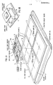
- Figure 3 shows an exploded view of the various elements involved in the multi-level interface used in accordance with the present invention.
- the encapsulated chip employs two levels of fine line metal patterns to perform chip I/O fanout and power distribution.
- the delete land (d) between contact wells (b) and (c) is shown on the single chip carrier.
- the second film level employs two levels of fine line metal patterns and is employed for power distribution and intra-connection of the 9-chip group.
- the relationship of the protrusion (G) to the delete land is clearly shown.
- two levels of fine line metal patterns are employed for intra-connection of a set of four 9-chip groups.
- the EC pads and EC apertures are shown on this 36-chip interface (N). Also shown is the power stripe coupling to the protrusions on the 9-chip interface (H).
- the equivalent printed board structure provides wiring between groups of the 36 chips. Accordingly, three film levels having 6 metal layers are used in this MLC structure.
- the wiring for the 36 chip structure is distributed through two plane pairs and is provided with three levels of laser delete and signal net repair via miniature thermo-compression bonded wires.
- a single chip on the single chip carrier or an entire 9-chip group may be designated for replacement.
- Replacement is effectuated by use of, for example, vacuum head with an appropriate perimeter mounted heating element.
- the multi-level wiring films are thin enough to permit viewing of embedded optical alignment marks to allow accurate placement of the head vis-a-vis that module designated for replacement.
- FIG. 4A The multi-level repairable system in accordance with this invention is compared in Figure 4 with a known TCM.
- the known system is shown in the exploded elevation view of FIG. 4A.
- This device is also defined in "Electronics", June 16, 1982, p. 145.
- the equivalent embodiment utilizing the concepts of this invention is shown in FIG. 4B.
- FIG. 4B also shows a first modification of the invention.
- encapsulated chip groups are mounted to both surfaces of the printed circuit board.
- the bottom surface shows the assembled multi-tiered arrangement while the top surface has the layers exploded away to show the individual components.
- Cooling studs (F) are directly attached to provide low thermal resistance pads into the immediate airflow stream.
- the dielectric constant for chip-to-chip is approximately 3.5 or lower.
- the 36-group to 36-group dielectric constant through the circuit board is approximately 4.6.
- the invention also provides extreme expansivity differential compensation since it can employ direct vapor deposition of Cr/Cu/Cr to the ball-limiting metallization pad. This extends along a membrane-like structure to a solderable connection point on the membrane but may extend beyond the edge of the silicon chip.
- the TCM shown in FIG. 4A employs five levels of the MLC for the chip footprint transformation to the wiring format.
- the multi-level interface in accordance with the present invention requires only two layers of polyimide.
- the dielectric constant of the polyimide is 3.5 as opposed to 9.4 for the ceramic in MLC.
- the TCM employs 6 plane pairs for wiring support. Equivalent wiring capacity is achieved in accordance with the present invention by using two photolithographic process plane pairs, the 9 and 36 chip carriers (H) and (N).
- the TCM requires a Harcon connector that in turn requires two via holes per signal contact element to effect a delete and EC capability on the far side of the circuit board.
- the multi-level interface of the present invention employs an integral multi-level repair capability that facilitates the placement of packaged electronics on both surfaces of the board.
- FIG. 4B illustrates a dual surface embodiment of the thin film structure shown in Figure 3.
- An assembly of film members comprising a single chip carrier of the 9-chip carrier (H) and the 36-chip carrier (N) are disposed on the printed circuit board on both sides.
- a retaining plate (P) covers the array of cooling studs (F) and is held in place by screws anchored in a stiffener (S).
- the stiffeners are disposed about the periphery of the 36-chip group. Accordingly, two separate 36-chip groups are disposed on opposite sides of the circuit board.
- the retaining plate (P) has, as shown in Figure 4B, a series of holes to allow the cooling studs (F) to protrude into the airflow stream. Tabs are placed about the perimeter of the retainer plate to allow adjacent retainer plates to share a common stiffener rib for purposes of mounting.
- the holes for the cooling studs are defined in a 6 x 6 array corresponding to the location of the studs above the 36-chip carrier.
- the retaining plate (P) has an elastomer backing for purposes of compressing the plate onto the assembly.
- a keeper plate having spring clips engaging the tops of the cooling studs may be employed to provide the necessary compression.
- the cooling studs (F) may alternatively be anchored by eliminating reflow soldering techniques to join the metal cap of the encapsulated chip.
- the studs are grooved to accept snap rings.
- the snap rings then anchor the cooling studs to the retainer plate. Since reflow solder coupling to the metal cap is not used, a thermal grease coating is applied to the contact surface of the cooling stud.
- An advantage in this technique is that the cooling stud is separable from the encapsulated chip and is made an integral part of the retainer plate.
- the elastomer material on the bottom of the retainer plate allows compression so that forced engagement of the cooling stud to the top of the encapsulated chip takes place.
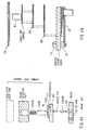
- Figure 5 illustrates another modification of this invention to allow the inclusion of a thin ceramic support member for effectuating mechanical support and additional printed wiring capabilities.
- a thin film wiring structure is processed on the surface of a thin ceramic support element.
- the thin ceramic is then laser scribed about its perimeter or along one edge thereof to allow for a subsequent breaking operation.
- the region within the laser scribed perimeter has a Cr/Cu/Cu interface with the thin film wiring structure.
- the region external the laser scribed perimeter has a Cr/Al interface with the thin film structure.
- the opposite surface of the thin ceramic can be processed utilizing known thick film techniques to effectuate power distribution patterns, including passive elements such as decoupling decapacitors or termination resistors.
- Via holes (L) and (M) are disposed in the Cr/Al interface.
- the aluminum is then dissolved at the interface of the ceramic and the thin film wiring structure and the ceramic segments outside the laser scribed regions are then broken off and discarded. This is shown in Figure 5B.
- the thin film member may then be deflected'for bonding to the next package level.
- a replacement wire for bonding to the next package level is preprocessed in the system. This is accomplished while providing the necessary mechanical support and stability necessary to build-u p device using the thick film. Also, the resulting metal film will not fold or wrinkle prior to use since it is supported by the thick film. Another advantage of this technique is that it provides a replacement wire that will easily compensate for physical size differences between layers. Naturally, it is possible to have the thin film member bonded to the next level of packaging without deflection by simply bonding directly to the next succeeding ceramic support element.
- a repairable multi-level overlay wiring system for semiconductor chips is defined.
- a unique packaging structure having exceptional versatility is defined.
Landscapes
- Wire Bonding (AREA)
- Semiconductor Integrated Circuits (AREA)
- Production Of Multi-Layered Print Wiring Board (AREA)
Applications Claiming Priority (2)
| Application Number | Priority Date | Filing Date | Title |
|---|---|---|---|
| US396204 | 1982-07-08 | ||
| US06/396,204 US4549200A (en) | 1982-07-08 | 1982-07-08 | Repairable multi-level overlay system for semiconductor device |
Publications (3)
| Publication Number | Publication Date |
|---|---|
| EP0098932A2 true EP0098932A2 (fr) | 1984-01-25 |
| EP0098932A3 EP0098932A3 (en) | 1986-09-17 |
| EP0098932B1 EP0098932B1 (fr) | 1990-01-17 |
Family
ID=23566285
Family Applications (1)
| Application Number | Title | Priority Date | Filing Date |
|---|---|---|---|
| EP83104479A Expired EP0098932B1 (fr) | 1982-07-08 | 1983-05-06 | Système à multi-niveaux réparable pour dispositif semi-conducteur |
Country Status (4)
| Country | Link |
|---|---|
| US (1) | US4549200A (fr) |
| EP (1) | EP0098932B1 (fr) |
| JP (1) | JPS5914660A (fr) |
| DE (1) | DE3381129D1 (fr) |
Cited By (6)
| Publication number | Priority date | Publication date | Assignee | Title |
|---|---|---|---|---|
| WO1988000396A1 (fr) * | 1986-06-30 | 1988-01-14 | Robert Bosch Gmbh | Appareil hybride a plaquettes multiples |
| EP0320660A3 (en) * | 1987-12-17 | 1989-08-09 | International Business Machines Corporation | Integrated circuit package |
| EP0638931A3 (fr) * | 1993-08-12 | 1995-05-10 | Fujitsu Ltd | Module à multi-puce. |
| EP0315792B1 (fr) * | 1987-11-06 | 1995-05-10 | Loral Aerospace Corporation | Système d'interconnexion pour puces de circuits intégrés |
| EP0649171A3 (fr) * | 1993-10-18 | 1995-10-11 | Hughes Aircraft Co | Module multi-puces avec interconnexion à décalcomanie fabriquée par l'intermédiaire d'une préforme. |
| KR101238255B1 (ko) * | 2004-08-19 | 2013-02-27 | 로베르트 보쉬 게엠베하 | 소형 캐리어가 구비된 디스크 브레이크 |
Families Citing this family (60)
| Publication number | Priority date | Publication date | Assignee | Title |
|---|---|---|---|---|
| US4727410A (en) * | 1983-11-23 | 1988-02-23 | Cabot Technical Ceramics, Inc. | High density integrated circuit package |
| US4672421A (en) * | 1984-04-02 | 1987-06-09 | Motorola, Inc. | Semiconductor packaging and method |
| FR2567709B1 (fr) * | 1984-07-11 | 1990-11-09 | Nec Corp | Ensemble a paillette comprenant un substrat de cablage multi-couche |
| JPS61296800A (ja) * | 1985-06-25 | 1986-12-27 | 日本電気株式会社 | 設計変更用電極 |
| US4689103A (en) * | 1985-11-18 | 1987-08-25 | E. I. Du Pont De Nemours And Company | Method of manufacturing injection molded printed circuit boards in a common planar array |
| US4681654A (en) * | 1986-05-21 | 1987-07-21 | International Business Machines Corporation | Flexible film semiconductor chip carrier |
| JPH0766253B2 (ja) * | 1986-06-20 | 1995-07-19 | 松下電器産業株式会社 | マトリクス型画像表示装置 |
| US4746815A (en) * | 1986-07-03 | 1988-05-24 | International Business Machines Corporation | Electronic EC for minimizing EC pads |
| US4945399A (en) * | 1986-09-30 | 1990-07-31 | International Business Machines Corporation | Electronic package with integrated distributed decoupling capacitors |
| US4744008A (en) * | 1986-11-18 | 1988-05-10 | International Business Machines Corporation | Flexible film chip carrier with decoupling capacitors |
| US4855867A (en) * | 1987-02-02 | 1989-08-08 | International Business Machines Corporation | Full panel electronic packaging structure |
| US4766670A (en) * | 1987-02-02 | 1988-08-30 | International Business Machines Corporation | Full panel electronic packaging structure and method of making same |
| US4788767A (en) * | 1987-03-11 | 1988-12-06 | International Business Machines Corporation | Method for mounting a flexible film semiconductor chip carrier on a circuitized substrate |
| US5159535A (en) * | 1987-03-11 | 1992-10-27 | International Business Machines Corporation | Method and apparatus for mounting a flexible film semiconductor chip carrier on a circuitized substrate |
| US5170931A (en) * | 1987-03-11 | 1992-12-15 | International Business Machines Corporation | Method and apparatus for mounting a flexible film semiconductor chip carrier on a circuitized substrate |
| USD312646S (en) | 1987-06-17 | 1990-12-04 | Sierra Research And Technology, Inc. | Electronic circuit board rework and repair system |
| US4918335A (en) * | 1987-11-06 | 1990-04-17 | Ford Aerospace Corporation | Interconnection system for integrated circuit chips |
| US4814283A (en) * | 1988-04-08 | 1989-03-21 | General Electric Company | Simple automated discretionary bonding of multiple parallel elements |
| US5014114A (en) * | 1988-09-30 | 1991-05-07 | Harris Corporation | High speed, high density semiconductor memory package with chip level repairability |
| US5122475A (en) * | 1988-09-30 | 1992-06-16 | Harris Corporation | Method of making a high speed, high density semiconductor memory package with chip level repairability |
| JP2751450B2 (ja) * | 1989-08-28 | 1998-05-18 | セイコーエプソン株式会社 | テープキャリアの実装構造及びその実装方法 |
| US5060116A (en) * | 1990-04-20 | 1991-10-22 | Grobman Warren D | Electronics system with direct write engineering change capability |
| US5224022A (en) * | 1990-05-15 | 1993-06-29 | Microelectronics And Computer Technology Corporation | Reroute strategy for high density substrates |
| US5124677A (en) * | 1990-08-22 | 1992-06-23 | Harris Corporation | Waffleline-configured surface-mount package for high frequency signal coupling applications |
| US5155577A (en) * | 1991-01-07 | 1992-10-13 | International Business Machines Corporation | Integrated circuit carriers and a method for making engineering changes in said carriers |
| EP0518701A3 (en) * | 1991-06-14 | 1993-04-21 | Aptix Corporation | Field programmable circuit module |
| US5261155A (en) * | 1991-08-12 | 1993-11-16 | International Business Machines Corporation | Method for bonding flexible circuit to circuitized substrate to provide electrical connection therebetween using different solders |
| US5243140A (en) * | 1991-10-04 | 1993-09-07 | International Business Machines Corporation | Direct distribution repair and engineering change system |
| US5208729A (en) * | 1992-02-14 | 1993-05-04 | International Business Machines Corporation | Multi-chip module |
| US5343366A (en) * | 1992-06-24 | 1994-08-30 | International Business Machines Corporation | Packages for stacked integrated circuit chip cubes |
| US5354955A (en) * | 1992-12-02 | 1994-10-11 | International Business Machines Corporation | Direct jump engineering change system |
| US5294754A (en) * | 1992-12-24 | 1994-03-15 | Iternational Business Machines Corporation | Direct write EC single metal layer |
| US5422514A (en) * | 1993-05-11 | 1995-06-06 | Micromodule Systems, Inc. | Packaging and interconnect system for integrated circuits |
| US5796164A (en) * | 1993-05-11 | 1998-08-18 | Micromodule Systems, Inc. | Packaging and interconnect system for integrated circuits |
| DE19605966A1 (de) * | 1996-02-17 | 1997-08-21 | Bosch Gmbh Robert | Vorrichtung, insbesondere zur Verwendung in einem elektronischen Steuergerät |
| KR100474002B1 (ko) | 1998-04-28 | 2005-07-18 | 엘지.필립스 엘시디 주식회사 | 액정표시장치의불량패드수리방법및그구조 |
| US6713854B1 (en) | 2000-10-16 | 2004-03-30 | Legacy Electronics, Inc | Electronic circuit module with a carrier having a mounting pad array |
| US7102892B2 (en) * | 2000-03-13 | 2006-09-05 | Legacy Electronics, Inc. | Modular integrated circuit chip carrier |
| US7337522B2 (en) * | 2000-10-16 | 2008-03-04 | Legacy Electronics, Inc. | Method and apparatus for fabricating a circuit board with a three dimensional surface mounted array of semiconductor chips |
| JP4484430B2 (ja) * | 2001-03-14 | 2010-06-16 | レガシー エレクトロニクス, インコーポレイテッド | 半導体チップの3次元表面実装アレイを有する回路基板を製造する方法 |
| US6954984B2 (en) * | 2002-07-25 | 2005-10-18 | International Business Machines Corporation | Land grid array structure |
| WO2004023859A1 (fr) | 2002-09-03 | 2004-03-18 | Pcb Plus, Inc. | Appareil et procede de remplacement de carte a circuit imprime defectueuse sur un panneau a cartes a circuits imprimes |
| WO2006076381A2 (fr) * | 2005-01-12 | 2006-07-20 | Legacy Electronics, Inc. | Carte de circuit radial, systeme et procedes |
| US7534966B2 (en) * | 2007-06-12 | 2009-05-19 | Clear Electronics, Inc. | Edge connection structure for printed circuit boards |
| US7741151B2 (en) * | 2008-11-06 | 2010-06-22 | Freescale Semiconductor, Inc. | Integrated circuit package formation |
| TWM362572U (en) * | 2009-04-13 | 2009-08-01 | Phytrex Technology Corp | Signal convertor |
| US9645603B1 (en) | 2013-09-12 | 2017-05-09 | Advanced Processor Architectures, Llc | System clock distribution in a distributed computing environment |
| US9429983B1 (en) | 2013-09-12 | 2016-08-30 | Advanced Processor Architectures, Llc | System clock distribution in a distributed computing environment |
| US8022526B2 (en) | 2009-08-07 | 2011-09-20 | Advanced Processor Architectures, Llc | Distributed computing |
| US11042211B2 (en) | 2009-08-07 | 2021-06-22 | Advanced Processor Architectures, Llc | Serially connected computing nodes in a distributed computing system |
| TWI461127B (zh) * | 2012-12-25 | 2014-11-11 | Univ Nat Taipei Technology | 電子裝置及其製法 |
| USD759022S1 (en) * | 2013-03-13 | 2016-06-14 | Nagrastar Llc | Smart card interface |
| USD729808S1 (en) | 2013-03-13 | 2015-05-19 | Nagrastar Llc | Smart card interface |
| USD758372S1 (en) * | 2013-03-13 | 2016-06-07 | Nagrastar Llc | Smart card interface |
| US9888283B2 (en) | 2013-03-13 | 2018-02-06 | Nagrastar Llc | Systems and methods for performing transport I/O |
| US9647997B2 (en) | 2013-03-13 | 2017-05-09 | Nagrastar, Llc | USB interface for performing transport I/O |
| USD780763S1 (en) | 2015-03-20 | 2017-03-07 | Nagrastar Llc | Smart card interface |
| USD864968S1 (en) | 2015-04-30 | 2019-10-29 | Echostar Technologies L.L.C. | Smart card interface |
| CN107770956A (zh) * | 2016-08-16 | 2018-03-06 | 光宝电子(广州)有限公司 | 电路板结构 |
| CN108615772B (zh) * | 2018-05-17 | 2020-05-12 | 中国科学院微电子研究所 | 传感器的封装结构与其制作方法 |
Family Cites Families (9)
| Publication number | Priority date | Publication date | Assignee | Title |
|---|---|---|---|---|
| US3777221A (en) * | 1972-12-18 | 1973-12-04 | Ibm | Multi-layer circuit package |
| US4069498A (en) * | 1976-11-03 | 1978-01-17 | International Business Machines Corporation | Studded heat exchanger for integrated circuit package |
| US4225900A (en) * | 1978-10-25 | 1980-09-30 | Raytheon Company | Integrated circuit device package interconnect means |
| US4254445A (en) * | 1979-05-07 | 1981-03-03 | International Business Machines Corporation | Discretionary fly wire chip interconnection |
| US4288841A (en) * | 1979-09-20 | 1981-09-08 | Bell Telephone Laboratories, Incorporated | Double cavity semiconductor chip carrier |
| JPS5687395A (en) * | 1979-12-18 | 1981-07-15 | Fujitsu Ltd | Semiconductor device |
| US4322778A (en) * | 1980-01-25 | 1982-03-30 | International Business Machines Corp. | High performance semiconductor package assembly |
| US4472762A (en) * | 1980-09-25 | 1984-09-18 | Texas Instruments Incorporated | Electronic circuit interconnection system |
| US4423468A (en) * | 1980-10-01 | 1983-12-27 | Motorola, Inc. | Dual electronic component assembly |
-
1982
- 1982-07-08 US US06/396,204 patent/US4549200A/en not_active Expired - Lifetime
-
1983
- 1983-05-06 DE DE8383104479T patent/DE3381129D1/de not_active Expired - Lifetime
- 1983-05-06 EP EP83104479A patent/EP0098932B1/fr not_active Expired
- 1983-05-17 JP JP58085186A patent/JPS5914660A/ja active Granted
Cited By (8)
| Publication number | Priority date | Publication date | Assignee | Title |
|---|---|---|---|---|
| WO1988000396A1 (fr) * | 1986-06-30 | 1988-01-14 | Robert Bosch Gmbh | Appareil hybride a plaquettes multiples |
| EP0315792B1 (fr) * | 1987-11-06 | 1995-05-10 | Loral Aerospace Corporation | Système d'interconnexion pour puces de circuits intégrés |
| EP0320660A3 (en) * | 1987-12-17 | 1989-08-09 | International Business Machines Corporation | Integrated circuit package |
| US4899208A (en) * | 1987-12-17 | 1990-02-06 | International Business Machines Corporation | Power distribution for full wafer package |
| EP0638931A3 (fr) * | 1993-08-12 | 1995-05-10 | Fujitsu Ltd | Module à multi-puce. |
| US5586006A (en) * | 1993-08-12 | 1996-12-17 | Fujitsu Limited | Multi-chip module having a multi-layer circuit board with insulating layers and wiring conductors stacked together |
| EP0649171A3 (fr) * | 1993-10-18 | 1995-10-11 | Hughes Aircraft Co | Module multi-puces avec interconnexion à décalcomanie fabriquée par l'intermédiaire d'une préforme. |
| KR101238255B1 (ko) * | 2004-08-19 | 2013-02-27 | 로베르트 보쉬 게엠베하 | 소형 캐리어가 구비된 디스크 브레이크 |
Also Published As
| Publication number | Publication date |
|---|---|
| EP0098932B1 (fr) | 1990-01-17 |
| JPH0512859B2 (fr) | 1993-02-19 |
| US4549200A (en) | 1985-10-22 |
| DE3381129D1 (de) | 1990-02-22 |
| EP0098932A3 (en) | 1986-09-17 |
| JPS5914660A (ja) | 1984-01-25 |
Similar Documents
| Publication | Publication Date | Title |
|---|---|---|
| US4549200A (en) | Repairable multi-level overlay system for semiconductor device | |
| US4991000A (en) | Vertically interconnected integrated circuit chip system | |
| US4472876A (en) | Area-bonding tape | |
| US5477933A (en) | Electronic device interconnection techniques | |
| US4251852A (en) | Integrated circuit package | |
| US6180881B1 (en) | Chip stack and method of making same | |
| US4446477A (en) | Multichip thin film module | |
| US7104804B2 (en) | Method and apparatus for memory module circuit interconnection | |
| US5032896A (en) | 3-D integrated circuit assembly employing discrete chips | |
| US6404043B1 (en) | Panel stacking of BGA devices to form three-dimensional modules | |
| US5343366A (en) | Packages for stacked integrated circuit chip cubes | |
| EP0863548B1 (fr) | Support pour circuit intégré et méthode de fabrication associée | |
| US5477082A (en) | Bi-planar multi-chip module | |
| US7180170B2 (en) | Lead-free integrated circuit package structure | |
| JP3669004B2 (ja) | プリント回路板を使用した電子部品パッケージの立体相互接続方法 | |
| US5155302A (en) | Electronic device interconnection techniques | |
| JPH07101728B2 (ja) | 多層配線構造体 | |
| JPH01132151A (ja) | 集積回路を相互接続するためのモジユ−ル | |
| WO1992003844A1 (fr) | Module de circuits integres multicouche | |
| EP0590915B1 (fr) | Assemblage des puces sur une carte | |
| EP0171232B1 (fr) | Ruban pour la soudure de surfaces | |
| US6437436B2 (en) | Integrated circuit chip package with test points | |
| KR100469543B1 (ko) | 반도체장치,반도체장치제조프로세스,다이입출력패턴재구성방법및다이-적응가능한반도체장치어셈블리설계방법 |
Legal Events
| Date | Code | Title | Description |
|---|---|---|---|
| PUAI | Public reference made under article 153(3) epc to a published international application that has entered the european phase |
Free format text: ORIGINAL CODE: 0009012 |
|
| AK | Designated contracting states |
Designated state(s): DE FR GB |
|
| 17P | Request for examination filed |
Effective date: 19840523 |
|
| PUAL | Search report despatched |
Free format text: ORIGINAL CODE: 0009013 |
|
| AK | Designated contracting states |
Kind code of ref document: A3 Designated state(s): DE FR GB |
|
| 17Q | First examination report despatched |
Effective date: 19880506 |
|
| GRAA | (expected) grant |
Free format text: ORIGINAL CODE: 0009210 |
|
| AK | Designated contracting states |
Kind code of ref document: B1 Designated state(s): DE FR GB |
|
| REF | Corresponds to: |
Ref document number: 3381129 Country of ref document: DE Date of ref document: 19900222 |
|
| ET | Fr: translation filed | ||
| PLBE | No opposition filed within time limit |
Free format text: ORIGINAL CODE: 0009261 |
|
| STAA | Information on the status of an ep patent application or granted ep patent |
Free format text: STATUS: NO OPPOSITION FILED WITHIN TIME LIMIT |
|
| 26N | No opposition filed | ||
| PGFP | Annual fee paid to national office [announced via postgrant information from national office to epo] |
Ref country code: GB Payment date: 19930427 Year of fee payment: 11 |
|
| PGFP | Annual fee paid to national office [announced via postgrant information from national office to epo] |
Ref country code: DE Payment date: 19930525 Year of fee payment: 11 |
|
| PGFP | Annual fee paid to national office [announced via postgrant information from national office to epo] |
Ref country code: FR Payment date: 19940427 Year of fee payment: 12 |
|
| PG25 | Lapsed in a contracting state [announced via postgrant information from national office to epo] |
Ref country code: GB Effective date: 19940506 |
|
| GBPC | Gb: european patent ceased through non-payment of renewal fee |
Effective date: 19940506 |
|
| PG25 | Lapsed in a contracting state [announced via postgrant information from national office to epo] |
Ref country code: DE Effective date: 19950201 |
|
| PG25 | Lapsed in a contracting state [announced via postgrant information from national office to epo] |
Ref country code: FR Effective date: 19960229 |
|
| REG | Reference to a national code |
Ref country code: FR Ref legal event code: ST |
|
| REG | Reference to a national code |
Ref country code: FR Ref legal event code: ST |