EP0099174A1 - Vorrichtung und Verfahren zum Überziehen von Durchgangslöchern - Google Patents
Vorrichtung und Verfahren zum Überziehen von Durchgangslöchern Download PDFInfo
- Publication number
- EP0099174A1 EP0099174A1 EP83303045A EP83303045A EP0099174A1 EP 0099174 A1 EP0099174 A1 EP 0099174A1 EP 83303045 A EP83303045 A EP 83303045A EP 83303045 A EP83303045 A EP 83303045A EP 0099174 A1 EP0099174 A1 EP 0099174A1
- Authority
- EP
- European Patent Office
- Prior art keywords
- chamber
- power electrode
- electrode
- gas
- electrical energy
- Prior art date
- Legal status (The legal status is an assumption and is not a legal conclusion. Google has not performed a legal analysis and makes no representation as to the accuracy of the status listed.)
- Withdrawn
Links
- 238000000034 method Methods 0.000 title claims abstract description 57
- 238000009792 diffusion process Methods 0.000 claims abstract description 22
- 239000000463 material Substances 0.000 claims abstract description 21
- 238000000151 deposition Methods 0.000 claims abstract description 20
- 230000007423 decrease Effects 0.000 claims description 8
- 230000002093 peripheral effect Effects 0.000 claims description 6
- 230000003247 decreasing effect Effects 0.000 claims description 3
- 230000003116 impacting effect Effects 0.000 claims 1
- 239000007789 gas Substances 0.000 abstract description 74
- 229910052751 metal Inorganic materials 0.000 abstract description 21
- 239000002184 metal Substances 0.000 abstract description 21
- RYGMFSIKBFXOCR-UHFFFAOYSA-N Copper Chemical compound [Cu] RYGMFSIKBFXOCR-UHFFFAOYSA-N 0.000 description 11
- 229910052802 copper Inorganic materials 0.000 description 11
- 239000010949 copper Substances 0.000 description 11
- 230000008021 deposition Effects 0.000 description 9
- 230000008569 process Effects 0.000 description 8
- 238000004544 sputter deposition Methods 0.000 description 6
- QAOWNCQODCNURD-UHFFFAOYSA-N Sulfuric acid Chemical compound OS(O)(=O)=O QAOWNCQODCNURD-UHFFFAOYSA-N 0.000 description 5
- KDLHZDBZIXYQEI-UHFFFAOYSA-N Palladium Chemical compound [Pd] KDLHZDBZIXYQEI-UHFFFAOYSA-N 0.000 description 4
- 230000004913 activation Effects 0.000 description 4
- 238000004140 cleaning Methods 0.000 description 4
- 238000004891 communication Methods 0.000 description 4
- 239000004020 conductor Substances 0.000 description 4
- 239000012530 fluid Substances 0.000 description 4
- 230000006872 improvement Effects 0.000 description 4
- 238000004519 manufacturing process Methods 0.000 description 4
- 239000000203 mixture Substances 0.000 description 4
- XLYOFNOQVPJJNP-UHFFFAOYSA-N water Substances O XLYOFNOQVPJJNP-UHFFFAOYSA-N 0.000 description 4
- HEMHJVSKTPXQMS-UHFFFAOYSA-M Sodium hydroxide Chemical compound [OH-].[Na+] HEMHJVSKTPXQMS-UHFFFAOYSA-M 0.000 description 3
- ATJFFYVFTNAWJD-UHFFFAOYSA-N Tin Chemical compound [Sn] ATJFFYVFTNAWJD-UHFFFAOYSA-N 0.000 description 3
- 238000007747 plating Methods 0.000 description 3
- IJGRMHOSHXDMSA-UHFFFAOYSA-N Atomic nitrogen Chemical compound N#N IJGRMHOSHXDMSA-UHFFFAOYSA-N 0.000 description 2
- MHAJPDPJQMAIIY-UHFFFAOYSA-N Hydrogen peroxide Chemical compound OO MHAJPDPJQMAIIY-UHFFFAOYSA-N 0.000 description 2
- 239000012190 activator Substances 0.000 description 2
- ROOXNKNUYICQNP-UHFFFAOYSA-N ammonium persulfate Chemical compound [NH4+].[NH4+].[O-]S(=O)(=O)OOS([O-])(=O)=O ROOXNKNUYICQNP-UHFFFAOYSA-N 0.000 description 2
- 239000000919 ceramic Substances 0.000 description 2
- 238000010276 construction Methods 0.000 description 2
- 239000003989 dielectric material Substances 0.000 description 2
- 229910001873 dinitrogen Inorganic materials 0.000 description 2
- 238000007772 electroless plating Methods 0.000 description 2
- 238000002474 experimental method Methods 0.000 description 2
- 239000012212 insulator Substances 0.000 description 2
- 229910052763 palladium Inorganic materials 0.000 description 2
- LCPVQAHEFVXVKT-UHFFFAOYSA-N 2-(2,4-difluorophenoxy)pyridin-3-amine Chemical compound NC1=CC=CN=C1OC1=CC=C(F)C=C1F LCPVQAHEFVXVKT-UHFFFAOYSA-N 0.000 description 1
- VEXZGXHMUGYJMC-UHFFFAOYSA-M Chloride anion Chemical compound [Cl-] VEXZGXHMUGYJMC-UHFFFAOYSA-M 0.000 description 1
- QPLDLSVMHZLSFG-UHFFFAOYSA-N Copper oxide Chemical compound [Cu]=O QPLDLSVMHZLSFG-UHFFFAOYSA-N 0.000 description 1
- 239000005751 Copper oxide Substances 0.000 description 1
- 239000004593 Epoxy Substances 0.000 description 1
- 230000003213 activating effect Effects 0.000 description 1
- 229910001870 ammonium persulfate Inorganic materials 0.000 description 1
- QVGXLLKOCUKJST-UHFFFAOYSA-N atomic oxygen Chemical compound [O] QVGXLLKOCUKJST-UHFFFAOYSA-N 0.000 description 1
- 230000009286 beneficial effect Effects 0.000 description 1
- 239000003054 catalyst Substances 0.000 description 1
- 239000003638 chemical reducing agent Substances 0.000 description 1
- 239000008139 complexing agent Substances 0.000 description 1
- 239000012141 concentrate Substances 0.000 description 1
- 230000001143 conditioned effect Effects 0.000 description 1
- 230000003750 conditioning effect Effects 0.000 description 1
- 230000001276 controlling effect Effects 0.000 description 1
- 229910000431 copper oxide Inorganic materials 0.000 description 1
- 229910000365 copper sulfate Inorganic materials 0.000 description 1
- ARUVKPQLZAKDPS-UHFFFAOYSA-L copper(II) sulfate Chemical compound [Cu+2].[O-][S+2]([O-])([O-])[O-] ARUVKPQLZAKDPS-UHFFFAOYSA-L 0.000 description 1
- 125000004122 cyclic group Chemical group 0.000 description 1
- 239000008367 deionised water Substances 0.000 description 1
- 229910021641 deionized water Inorganic materials 0.000 description 1
- 238000005553 drilling Methods 0.000 description 1
- 238000001035 drying Methods 0.000 description 1
- 238000009713 electroplating Methods 0.000 description 1
- 239000004519 grease Substances 0.000 description 1
- 150000008282 halocarbons Chemical class 0.000 description 1
- 238000007654 immersion Methods 0.000 description 1
- 238000003780 insertion Methods 0.000 description 1
- 230000037431 insertion Effects 0.000 description 1
- WSFSSNUMVMOOMR-NJFSPNSNSA-N methanone Chemical compound O=[14CH2] WSFSSNUMVMOOMR-NJFSPNSNSA-N 0.000 description 1
- 238000012986 modification Methods 0.000 description 1
- 230000004048 modification Effects 0.000 description 1
- 238000009828 non-uniform distribution Methods 0.000 description 1
- 239000001301 oxygen Substances 0.000 description 1
- 229910052760 oxygen Inorganic materials 0.000 description 1
- 239000002245 particle Substances 0.000 description 1
- JRKICGRDRMAZLK-UHFFFAOYSA-L persulfate group Chemical group S(=O)(=O)([O-])OOS(=O)(=O)[O-] JRKICGRDRMAZLK-UHFFFAOYSA-L 0.000 description 1
- 230000001105 regulatory effect Effects 0.000 description 1
- 238000011160 research Methods 0.000 description 1
- 229920006395 saturated elastomer Polymers 0.000 description 1
- 238000005201 scrubbing Methods 0.000 description 1
- CHQMHPLRPQMAMX-UHFFFAOYSA-L sodium persulfate Substances [Na+].[Na+].[O-]S(=O)(=O)OOS([O-])(=O)=O CHQMHPLRPQMAMX-UHFFFAOYSA-L 0.000 description 1
- 239000008399 tap water Substances 0.000 description 1
- 235000020679 tap water Nutrition 0.000 description 1
- 238000012546 transfer Methods 0.000 description 1
- 238000013022 venting Methods 0.000 description 1
Images



Classifications
-
- H—ELECTRICITY
- H05—ELECTRIC TECHNIQUES NOT OTHERWISE PROVIDED FOR
- H05K—PRINTED CIRCUITS; CASINGS OR CONSTRUCTIONAL DETAILS OF ELECTRIC APPARATUS; MANUFACTURE OF ASSEMBLAGES OF ELECTRICAL COMPONENTS
- H05K3/00—Apparatus or processes for manufacturing printed circuits
- H05K3/40—Forming printed elements for providing electric connections to or between printed circuits
- H05K3/4038—Through-connections; Vertical interconnect access [VIA] connections
- H05K3/4076—Through-connections; Vertical interconnect access [VIA] connections by thin-film techniques
-
- C—CHEMISTRY; METALLURGY
- C23—COATING METALLIC MATERIAL; COATING MATERIAL WITH METALLIC MATERIAL; CHEMICAL SURFACE TREATMENT; DIFFUSION TREATMENT OF METALLIC MATERIAL; COATING BY VACUUM EVAPORATION, BY SPUTTERING, BY ION IMPLANTATION OR BY CHEMICAL VAPOUR DEPOSITION, IN GENERAL; INHIBITING CORROSION OF METALLIC MATERIAL OR INCRUSTATION IN GENERAL
- C23C—COATING METALLIC MATERIAL; COATING MATERIAL WITH METALLIC MATERIAL; SURFACE TREATMENT OF METALLIC MATERIAL BY DIFFUSION INTO THE SURFACE, BY CHEMICAL CONVERSION OR SUBSTITUTION; COATING BY VACUUM EVAPORATION, BY SPUTTERING, BY ION IMPLANTATION OR BY CHEMICAL VAPOUR DEPOSITION, IN GENERAL
- C23C14/00—Coating by vacuum evaporation, by sputtering or by ion implantation of the coating forming material
- C23C14/04—Coating on selected surface areas, e.g. using masks
- C23C14/046—Coating cavities or hollow spaces, e.g. interior of tubes; Infiltration of porous substrates
Definitions
- This invention relates to a plated-through-hole apparatus and method. More particularly, this invention relates to an apparatus and method for depositing a thin layer of metal onto the entire inside surface of a hole in an object.
- the four different types of printed circuit boards are single sided boards, double sided boards, multi-layered boards, and flexible boards. Except for single sided boards and single sided flexible boards, it is necessary to provide electrical continuity via the holes in the boards, between the conductive pattern on each side of the board. This is accomplished by plating a layer of conductive material onto the inside surface of the hole in the board, and is referred to as the plated-thru-hole operation of the manufacturing process.
- the only presently available plated-thru-hole methods consist of electrolytic plating, electroless plating, and immersion plating. Each of these methods have their own particular advantages and disadvantages which largely depends on the type of printed circuit board being treated.
- electroless plating which is probably the most widely commercially used method, basically comprises subjecting the boards to a cleaning procedure, an activation procedure, and then a copper deposition procedure. More particularly, the cleaning procedure includes cleaning the boards with an alkaline cleaner to remove light oil and grease, fingerprints, etc.
- the holes in the boards are then "conditioned" to accept activation and subsequent electroless copper deposition.
- the conditioning of the holes involves removing epoxy smear caused by the drilling operation. Drill smear can be removed from within the holes by utilizing an -tchback process, or by utilizing my novel plasma desmearing apparatus and method which is disclosed in my copending application, Serial No. 253,007, filed April 10, 1981, the disclosure of which is hereby incorporated by reference.
- the holes are preetched by using ammonium persulfate, sodium persulfate, or hydrogen peroxide/sulfuric acid. This removes copper oxide and etches the copper to a uniform matte finish.
- the boards are dipped into sulfuric acid to remove any persulfate residues which would interfere with adhesion. The boards are then thoroughly rinsed in water to remove any sulfuric acid residues. This completes the cleaning procedure of the plated-thru-hole operation.
- the activation procedure comprises subjecting the boards to a preactivator (pre-dip) and then an activator (catalyst) which seeds particles of tin/palladium onto the nonconductive holes in order to provide a basis for subsequent electroless copper deposition. After one or more water rinses, the boards are immersed in an accelerator which dissolves the tin from the tin/palladium complex that was deposited in the holes by the activator. The activation procedure is completed by thoroughly rinsing the boards with tap water or deionized water.
- the copper deposition procedure comprises immersing the boards into an electroless copper bath which contains copper sulfate or chloride, sodium hydroxide, a reducing agent such as formaldehyde, and a complexing agent which holds the copper in solution.
- the boards remain in the copper bath for an appropriate length of time (depending on the desired thickness of the deposited layer of copper), and are removed and rinsed in water. After scrubbing and drying the boards, the boards are ready for the image transfer operation.
- electroless copper deposition is an extremely lengthy process. Moreover, the multitude of variables involved in the process makes the process more an art than a science, and results in nonuniform deposition of the copper within the holes of the printed circuit boards.
- Another object of this invention is to provide an apparatus and method for depositing a material onto an object by using plasma gas techniques.
- Another object of this invention is to provide an apparatus and method for depositing a material on the surface of an object in a controlled process with a high level of precise repeatability and at cyclic rates substantially reducing the overall cost of the process.
- Another object of this invention is to provide an apparatus and method for depositing the material uniformly on the surface of the object.
- the invention comprises a plated-thru-hole apparatus and method which deposits a thin layer of metal within the hole of an object such as a printed circuit board.
- the apparatus of the invention includes a chamber having a gas diffusion chamber connected to each end thereof. Means are provided for introducing a gas or a mixture of gases into one or both of the gas diffusion chambers and into the central area of the chamber itself.
- a vacuum pump is connected in fluid communication with the gas diffusion chambers for evacuating the chamber and for producing the desired flow of the gas in one direction and then in the other direction within the chamber.
- a plurality of power electrodes are positioned within the chamber transverse to the direction of the flow of the gases.
- the objects to be treated such as the printed circuit boards are then inserted into the areas between the power electrodes.
- the output of a generator means is connected to the power electrodes for supplying electrical energy thereto.
- the outer conductive layers of the printed circuit boards being treated are then connected to the ground of the generator means to complete the path of the electrical energy.
- the method of the invention basically comprises introducing the desired gases into one of the diffusion chambers while creating a reduced pressure in the other gas diffusion chamber such that the gas is drawn through the power electrodes and the printed circuit boards.
- the direction of the flow of the gas is then reversed by introducing the gas into the other gas diffusion chamber and creating a reduced pressure in the opposite gas diffusion chamber.
- the generator means supplies an amount of electical energy to the power electrodes.
- the gas is excited to a plasma state as the gas flows through apertures in the power electrodes.
- a portion of the material constituting the power electrode is sputtered into the holes of the printed circuit boards. The process is continued until the entire inside surface of the holes is uniformly coated with the material constituting the power electrode.
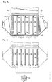
- Fig. 1 is a plan view of the plated-thru-hole apparatus 10 of the invention designed to deposit a thin layer of material such as a metal 12 on the inside surface of a hole 14 in an object such as a double-sided, multi-layered, or flexible printed circuit board 16. More particularly, the apparatus 10 comprises a substantially rectangular chamber 18. A frustopyramidal diffusion chamber 20 is connected to the left side of the chamber 18 (see Fig. 2). Similarly, another frustopyramidal diffusion chamber 22 is connected to the right side of the chamber 18. A left and a right exhaust conduit 24 and 26 are respectively connected in fluid communication with the diffusion chambers 20 and 22 and are orientated to extend rearwardly of the chamber 18.
- a frustopyramidal diffusion chamber 20 is connected to the left side of the chamber 18 (see Fig. 2).
- another frustopyramidal diffusion chamber 22 is connected to the right side of the chamber 18.
- a left and a right exhaust conduit 24 and 26 are respectively connected in fluid communication with the diffusion chambers
- the two exhaust conduits 24 and 26 then extend laterally of the chamber 18 and are each connected to a vacuum pump 28 by a tee conduit 30.
- vacuum pump 28 comprises a Stokes Pennwalt vacuum pump, Model 1736, with halocarbon oil for oxygen service which is capable of exhausting the chamber 18 to approximately 11 microns at a rate of 650 cubic feet per minute.
- a solenoid operated air valve 32 is connected to the rear of the chamber 18 for venting atmospheric air into the chamber 18 to normalize the pressure in the chamber 18.
- a left and a right exhaust valve 34 and 36 are connected in fluid communication with the left and right exhaust conduits 24 and 26, respectively.
- each of the exhaust valves 34 and 36 comprises a Vacuum Research Corporation exhaust valve, Model 6AV, which is air activated at 60 p.s.i. and which is solenoid controlled.
- the plated-thru-hole apparatus 10 of the invention further includes means for supplying a mixture of gases to the chamber 18. More particularly, a plurality of gas bottles 38 are provided for storing a particular gas identified as gases A through E inclusive.
- the output of each of the gas bottles 38 is connected to a gas manifold 40.
- the amount of gas supplied from the bottles 38 to the gas manifold 40 is controlled by means of electrically operated valves 42A-E, or the like.
- the output of the gas manifold 40 is then connected to a left and a right supply conduit 44 and 46 which are in turn connected in fluid communication with the diffusion chambers 20 and 22, respectively.
- a middle supply conduit 48 similarly extends from the gas manifold 40 to the central area of the chamber 18.
- Suitable control valves 50, 52, and 54 are connected within the conduits 44, 46, 48, respectively, to control the flow of gas into the chamber 18.
- a lid 56 is secured about the opened end of the chamber 18.
- the lid 56 comprises a substantially rectangular configuration which is dimensioned to fit over the opened end of the chamber 18.
- a gasket 58 is positioend about the periphery of the opened end of the chamber 18 enabling the lid 56 to seal about the opened end of the chamber 18 (see Fig. 3).
- Suitable latches 60 are positioned at opposing ends of the chamber 18 to rigidly secure the lid 56 in the closed position.
- the lid 56 is operatively connected to a pair of rails 62 and 64 which extend rearwardly of the chamber 18 such that the lid 56 may be slid rearwardly away from the opened end of the chamber 18 to an open position.
- Fig. 3 is a plan view of the chamber 18 showing the interior thereof. More particularly, a plurality of power electrodes 66 are uniformly suspended within the chamber 18 by means of a plurality of electrically insulative standoffs 68 which are rigidly secured to each of the power electrodes 66 about the sides and bottom thereof. The standoffs 68 are then rigidly secured to the inside surface of the chamber 18 such that the power electrodes 66 extend traversely across the longitudinal length of the chamber 18 .
- a source of electrical energy hereinafter referred to as a generator 70
- a generator 70 for supplying electrical energy to the power electrodes 66 to create a plasma gas in the chamber 18.
- the output of the generator 70 is connected to the power electrodes 66 by a coaxial cable or the like.
- the ground of the generator 70 is then connected to the chamber 18 and to the printed circuit board 16.
- the generator 70 may comprise a d.c. generator for supplying electrical energy at a constant rate and power level to the power electrode 66.
- the generator 70 may comprise a frequency generator for supplying electrical energy at a predetermined frequency and power level to the power electrode 66.
- the cross-sectional area of the chamber 18 preferably comprises a configuration substantially identical to the configuration of the object 16 to be treated.
- the cross-sectional area of the chamber 18 preferably comprises a configuration substantially identical to the configuration of the object 16 to be treated.
- the power electrodes 66 are preferably uniformly spaced apart from one another and possibly from the sides of the chamber 18 to define receiving areas 72 for receiving one or more printed circuit boards 16.
- the method of the invention for depositing a material such as a metal 12 on the inside surface of the holes 14 contained within the printed circuit boards 16 comprise the following steps. First, the lid 56 is slid rearwardly along the rails 62 and 64 to expose the opened end of the chamber 18. The printed circuit boards 16 are then inserted into the chamber 18 between adjoining power electrodes 66. In the specific embodiment of the chamber 18 which contains three power electrodes 66, shown diagrammatically in Fig. 4, four printed circuit boards 16 are inserted within the chamber 18 such that only one printed circuit board 16 is positioned within each receiving area 72. It should be understood, however, that a plurality of printed circuit boards 16 may be inserted within each receiving area 72 without departing from the spirit and scope of this invention.
- the next step of the method includes grounding the outer conductive layers 74 of the printed circuit board 16 to the ground of the generator 70.
- the lid 56 is slid forwardly along rails 62 and 64 to a closed position over the opened end of the chamber 18. Latches 60 are then tightened to sealingly secure the lid 56 in the closed position.
- the printed circuit boards 16 are now ready to receive the treatment of deposition of the metal 12 in the holes 14 contained in the printed circuit boards 16.
- the plated-thru-hole portion of the method of the invention comprises first activating the vacuum pump 28 to evacuate the interior of the chamber 18.
- a desired blend of gases is then selected by controlling valves 42A-E which regulate the selection and the flow rate of the gases contained within the gas bottles 38A-E into the gas manifold 40.
- the method proceeds by closing the right exhaust valve 36 and opening the right control valve 52 of the right supply conduit 46 while opening the left exhaust valve 34 and closing the left control valve 50 and the middle control valve 54. This causes the selected blend of gases to flow into the right diffusion chamber 22 wherein the gases are uniformly diffused over the cross-sectional area of the chamber 18.
- the reduced pressure created by the vacuum pump 28 which is supplied to the left exhaust valve 34 draws the gases from the right supply conduit 46 to the left exhaust valve 34 such that the gases flow serially through apertures in the power electrodes 66 and the holes 14 in the printed circuit boards 16 from right to left.
- the flow of the gases is reversed by closing the left exhaust valve 34 and opening the right exhaust valve 36, and opening the left control valve 50 and closing the right and middle control valves 52 and 54.
- the vacuum present at the right exhaust valve 36 draws the gases, which are injected into and diffused in the left diffusion chamber 20, serially through the power electrodes 66 and the printed circuit boards 16 in the reverse direction.
- the generator 70 is activated to supply electrical energy to the power electrodes 66.
- the gases flowing through the apertures in the power electrodes 66 are therefore excited to a plasma state.
- the power electrodes 66 being at least partially composed of the type of material such as the metal 12 to be deposited on the inside of the holes 14 of the printed circuit boards 16, a portion of such metal 12 will be "sputtered" from the power electrodes 66 into the holes 14 (and onto all exposed surfaces) of the printed circuit board 16 adjacent to the power electrode 66.
- the thickness of the layer of metal 12 deposited in the holes 14 of the printed circuit boards 16 will be progressively increased each time the above procedure is repeated.
- More uniform plating can be achieved by alternating the direction of the flow of the gas through the power electrodes 66 and the printed circuit boards 16.
- the plated-thru-hole portion of the method of the invention is completed when the desired thickness of the layer of metal in the hole has been achieved.
- a thickness of 25-to-100 microns is usually adequate.
- the next portion of the method of the invention comprises the steps of opening both of the exhaust valves 34 and 36 and injecting nitrogen gas into the chamber 18 via control valves 50, 52, and 54.
- air valve 32 is opened to vent atmospheric air into the chamber 18.
- the lid 56 is then slid rearwardly -along rails 62 and 64 to an open position.
- the treated printed circuit boards 16 are then removed from the chamber 18 thereby completing the method of the invention.
- the printed circuit boards 16 are now ready for further treatment of the manufacturing process.
- control valves 50 and 52 may be controlled to pulsate on and off to create a pulsating flow of gas in one direction through the electrodes 66 and the printed circuit boards 16, and then create another pulsating flow of gas in the other direction through the power electrodes 66 and the printed circuit boards 16.
- the method of the invention further contemplates the introduction of gas from the middle supply conduit 48 into the chamber 18 via control valve 54.
- control valve 54 inasmuch as the gas being introduced via control valve 54 will not be subjected to the diffusing characteristics of the diffusion chambers 20 and 22, the use of the middle control valve 54 should be limited to introducing.a small amount of gas into the chamber 18 to compensate for any depletion of the plasma gas therein.
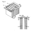
- FIG. 6 illustrates a unique printed circuit board rack 76 which enables a plurality of printed circuit boards 16 to be quickly and easily loaded within the chamber 18 and then subsequently unloaded after treatment.
- the rack 76 comprises a substantially rectangular frame member 78 having a number of groups of retainer clips 80 secured to the underside thereof.
- Each of the retainer clips 80 comprise a left and right member 82 and 84 which are resiliently biased toward one another.
- the individual printed circuit boards 16 are secured to the underside of the frame member 78 by pushing the edges of the printed circuit boards 16 between the members 82 and 84 of the respective retainer clip 80.
- the rack 76 is lifted by hand or by a hoist, positioned over the opened end of the chamber 18, and then lowered into the chamber 18 such that the groups of the retainer clips 80 and correspondingly, the group of installed printed circuit boards 16, are positioned between the power electrodes 66.
- a flange member (not shown) is connected to each of the sides'of the chamber 18 to enable the frame member 78 of the rack 76 to seat thereon, rather than on top of the power electrodes 66.
- the groups of retainer clips 80 must be spaced sufficiently apart such that the corresponding groups of printed circuit boards . 16 will straddle, and not touch the power electrodes 66 as the groups of installed printed circuit boards 16 are loaded into their respective receiving area 72. It is also noted that the members 82 and 84 of the retainer clips 80, the frame 78 of the rack 76, and the flange secured within the chamber 18 are each composed of an electrically conductive material such that the outer conductive layers of the printed circuit boards 16 will be electrically connected to the chamber 18 which is in turn connected to the ground of the generator 70. Thus, it should be appreciated that the rack 76, in addition to facilitating the loading of the printed circuit board 16 in the chamber 18, provides a convenient means for grounding the printed circuit boards 16 to the ground of the generator 70.
- FIG. 7 is a diametric view of an improvement which compensates for any saturation of the plasma gas which may occur as the plasma gas flows from one end of the chamber 18 to the other.
- this improvement includes providing three generators 70A, 70B, and 70C, the output of which are respectively connected to the power electrodes 66A, 66B, and 66C.
- Each of the generators 70A-C may individually comprise a d.c. generator or a frequency generator and may be individually regulated to supply the same or differing amounts of electrical energy to their respective power electrodes 66A-C.
- the amount of sputtering of the metal 12 from the power electrodes 66 to the respective printed circuit boards 16 installed within the chamber 18 is a function of the exposed surface area of the power electrodes 66 and the amount of electrical energy supplied to the power electrodes 66 per unit area (for example, watts per square inch).
- the saturation of the plasma gas as the plasma gas flows from one end of the chamber to the other is easily compensated for by increasing the amount of electrical energy supplied to succeeding power electrodes 66.
- the sputtering of the metal 12 from the power electrodes 66 tend to concentrate more in the holes 14 located in the outer periphery of the printed circuit boards 16 than in those holes 14 located near the center portion of the printed circuit boards 16.
- an improved power electrode identified in the drawings by the numeral 86, compensates for this nonuniform sputtering of the metal therefrom by increasing the amount of exposed surface area or the power density from the center portion to the outer peripheral edges of the power electrode 86.
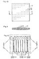
- the first embodiment of the improved electrode 86 as shown in Figs. 8 and 9 comprises incorporating a nonuniform distribution of the apertures 88 in the improved power electrode 86 such that the porosity of the improved power electrode 86 decreases from the central to the outer peripheral edges thereof. This results in a decreasing rate of exposed surface area from the central to the outer peripheral edges of the improved electrode 86.
- that portion of the plasma gas which flows through the apertures 88 in the center portion of the improved electrode 86 will be exposed to a greater surface area than the other portion of the plasma gas which flows through apertures 88 located in the outer portions of the improved power electrode 86.
- the same result may be accomplished by progressively decreasing or increasing the diameter of the apertures 88 from the center to the outer portions of the improved power electrode 86. It can be shown mathematically that the greatest exposed surface area occurs when the diameter of the apertures 88 decreases or increases from being equal to the thickness of the electrode 86. Thus, the diai,-eter-equal-to-thickness apertures 88 in the center portion of the improved power electrode 86 will provide an increased surface area over the other smaller (or larger) diameter apertures 88 located in the outer peripheral edges of the improved power electrode 86.
- Figs. 10 and 11 illustrate another embodiment of the improved power electrode 86 which compensates for the nonuniform sputtering of the metal 12 from the improved power electrode 86 into the holes 14 in the printed circuit boards 16.
- This second embodiment of the improved power electrode 86 is manufactured from a sheet of the metal 12, the opposing sides of which are convexed outwardly such that the cross-sectional configuration of the improved power electrode 86 progressively decreases from the center to the outer portion thereof.
- the length of the apertures 88 in the improved power electrode 86 and the exposed surface area thereof will progressively decrease from the center to the outer portions of the power electrode 86.
- Figs. 12 and 13 are a side view and a cross-sectional view, respectively, of the third embodiment of the improved power electrode 86.
- the third embodiment of the improved power electrode 86 comprises a central electrode 90 which is positioned within a drilled out center portion of an outer electrode 92.
- a suitable dielectric 94 such as a ceramic insulator is positioned within the air space between the central and the outer electrodes 90 and 92 to prevent arcing thereacross.
- Figs 14 and 15 are a side view and a cross-sectional view of the fourth embodiment of the improved power electrode 86 which is a modification of the third embodiment shown in Figs. 12 and 13.
- the fourth embodiment of the improved power electrode 86 comprises a central electrode 96 positioned within the center of a middle electrode 98, which is in turn positioned within the center of an outer electrode 100.
- Two dielectrics 102 and 104 such as ceramic insulators are respectively positioned between the central electrode 96 and the middle electrode 98, and the middle electrode 98 and the outer electrode 100 to prevent arcing therebetween.
- a grounding wire represented by numerals 106, 108, and 110 may be molded within each of the respective dielectrics 94, 102, and 104 and connected to the ground of the system to ground any arcing which may occur between the respective electrodes 90 and 92, and 96, 98, and 100.
- electrical energy is supplied individually to the central and the outer electrodes 90 and 92 by means of two corresponding generators 112A and 112B.
- the power level of each of the generators l12A and 112B are individually controlled such that a greater amount of electrical energy is supplied to the central electrode 90 than to the outer electrode 92. This assures that the plasma gas flowing through the apertures in the central electrode 90 will be excited to a higher plasma state than the other portion of the gas flowing through the apertures in the outer electrode 92. Uniform sputtering of the metal 12 from the electrodes 90 and 92 into the holes 14 of the printed circuit boards 16 will therefore be achieved.
- the use of the two generators 112A and 112B also provides for supplying electrical energy at separate or the same frequency to the central and outer electrodes 90 and 92.
- Fig. 14 illustrates the output of a single generator 114 being connected to each of the electrodes 98, 100, and 102 of the improved power electrode 86 by conductors 116A, 116B, and 116C.
- Attenuators 118A, 118B, and 118C are respectively interconnected within the conductors 116A, 116B, and 116C to individually attenuate the power level of the electrical energy being supplied from the generator 114 to the electrodes 96, 98, and 100.
- a greater power density of the electrical energy may be achieved on the central electrode 96 than on the middle electrode 98, and on the middle electrode 98 than the outer electrode 100. It is noted that unlike the generators 112A and 112B described in conjunction with the third embodiment of the improved power electrode 86, the use of a single generator 114 together with the attenuators 118A-C in the fourth embodiment of the improved power electrode 86 precludes the supply of electrical energy at different frequencies to the individual electrodes 96, 98, and 100.
- individual generators may be electrically connected to the electrodes 96, 98, and 100 such that not only different power levels may be supplied to the individual electrodes 96, 98, and 100, but also electrical energy at different frequencies may be supplied to the individual electrodes 96, 98, and 100.
- Fig. 16 is a diagrametric view of the apparatus 10 of the inventions incorporated within my desmearing apparatus which is more particularly disclosed in my copending patent applications, Serial Nos. 204,329 and 253,007, filed on November 4, 1980, and April 10, 1981, respectively, entitled "Plasma Desmearing Apparatus and Method” and which are hereby incorporated by reference into this application.
- my prior inventions comprised a plurality of electrode pairs 120 which were uniformly spaced within a chamber or the like. Each electrode pair comprised a power electrode 122 spaced an appreciable distance apart from a ground electrode 124.
- a generator 126 was then connected to the power electrode 122, with the ground electrode 124 being connected to the ground of the generator 126.
- Fig. 14 it is shown that two such electrode pairs 120 are positioned within the chamber 18 of my present invention. Then, three of the power electrodes 66 of the present invention are equally spaced within the distance between the electrode pairs 120. Two printed circuit boards 16 are then inserted between the power electrodes 66 in the respective receiving areas 72.
- the first step of the treatment of the printed circuit boards 16 involves desmearing the holes 14 contained therein according to my prior inventions. Then, the holes 14 in the printed circuit boards 16 are plated-through by using the method of my present invention.
Landscapes
- Engineering & Computer Science (AREA)
- Chemical & Material Sciences (AREA)
- Manufacturing & Machinery (AREA)
- Microelectronics & Electronic Packaging (AREA)
- Chemical Kinetics & Catalysis (AREA)
- Materials Engineering (AREA)
- Mechanical Engineering (AREA)
- Metallurgy (AREA)
- Organic Chemistry (AREA)
- Printing Elements For Providing Electric Connections Between Printed Circuits (AREA)
- Physical Vapour Deposition (AREA)
- Manufacturing Of Printed Wiring (AREA)
Applications Claiming Priority (2)
| Application Number | Priority Date | Filing Date | Title |
|---|---|---|---|
| US383311 | 1982-05-28 | ||
| US06/383,311 US4474659A (en) | 1982-05-28 | 1982-05-28 | Plated-through-hole method |
Publications (1)
| Publication Number | Publication Date |
|---|---|
| EP0099174A1 true EP0099174A1 (de) | 1984-01-25 |
Family
ID=23512572
Family Applications (1)
| Application Number | Title | Priority Date | Filing Date |
|---|---|---|---|
| EP83303045A Withdrawn EP0099174A1 (de) | 1982-05-28 | 1983-05-26 | Vorrichtung und Verfahren zum Überziehen von Durchgangslöchern |
Country Status (3)
| Country | Link |
|---|---|
| US (1) | US4474659A (de) |
| EP (1) | EP0099174A1 (de) |
| JP (1) | JPS58223400A (de) |
Cited By (3)
| Publication number | Priority date | Publication date | Assignee | Title |
|---|---|---|---|---|
| EP0188206B1 (de) * | 1985-01-17 | 1989-12-27 | International Business Machines Corporation | Einrichtung zur Erzeugung eines im wesentlichen homogenen Plasmas |
| EP0490469A1 (de) * | 1990-12-07 | 1992-06-17 | Brunswick Corporation | Methode zur Verringerung der Maschenweite eines feinmaschigen Siebes |
| WO1998032154A1 (en) * | 1997-01-17 | 1998-07-23 | Balzers Aktiengesellschaft | Capacitively coupled rf-plasma reactor |
Families Citing this family (20)
| Publication number | Priority date | Publication date | Assignee | Title |
|---|---|---|---|---|
| KR900001825B1 (ko) * | 1984-11-14 | 1990-03-24 | 가부시끼가이샤 히다찌세이사꾸쇼 | 성막 지향성을 고려한 스퍼터링장치 |
| US4681649A (en) * | 1985-04-15 | 1987-07-21 | Fazlin Fazal A | Multi-layer printed circuit board vacuum lamination method |
| US4828668A (en) * | 1986-03-10 | 1989-05-09 | Semiconductor Energy Laboratory Co., Ltd. | Sputtering system for deposition on parallel substrates |
| NL8601824A (nl) * | 1986-07-11 | 1988-02-01 | Hauzer Holding | Werkwijze en inrichting voor het met een geleidend plasmakanaal ontsteken van een boog. |
| US4885074A (en) * | 1987-02-24 | 1989-12-05 | International Business Machines Corporation | Plasma reactor having segmented electrodes |
| DE3854792D1 (de) * | 1987-02-24 | 1996-02-01 | Ibm | Plasmareaktor |
| US4913789A (en) * | 1988-04-18 | 1990-04-03 | Aung David K | Sputter etching and coating process |
| JP2604853B2 (ja) * | 1989-05-25 | 1997-04-30 | 松下電工株式会社 | 回路板のスルーホール形成方法 |
| JPH0449523A (ja) * | 1990-06-18 | 1992-02-18 | Denki Kagaku Kogyo Kk | 磁気記録媒体の製造法及びその装置 |
| US5415753A (en) * | 1993-07-22 | 1995-05-16 | Materials Research Corporation | Stationary aperture plate for reactive sputter deposition |
| US5670415A (en) * | 1994-05-24 | 1997-09-23 | Depositech, Inc. | Method and apparatus for vacuum deposition of highly ionized media in an electromagnetic controlled environment |
| EP1387602A1 (de) * | 2002-07-31 | 2004-02-04 | Fox Technologies S.r.l. | Verfahren zum Herstellen einer elektrisch leitenden Beschichtung auf Substraten für Leiterplatten |
| KR20060115734A (ko) * | 2003-10-28 | 2006-11-09 | 노드슨 코포레이션 | 플라즈마 프로세싱 시스템 및 플라즈마 처리 방법 |
| US8097133B2 (en) * | 2005-07-19 | 2012-01-17 | Applied Materials, Inc. | Evacuable magnetron chamber |
| US7976908B2 (en) * | 2008-05-16 | 2011-07-12 | General Electric Company | High throughput processes and systems for barrier film deposition and/or encapsulation of optoelectronic devices |
| US8372238B2 (en) * | 2008-05-20 | 2013-02-12 | Nordson Corporation | Multiple-electrode plasma processing systems with confined process chambers and interior-bussed electrical connections with the electrodes |
| US8226795B2 (en) * | 2009-02-03 | 2012-07-24 | Nordson Corporation | Magnetic clips and substrate holders for use in a plasma processing system |
| US9324597B2 (en) * | 2010-04-30 | 2016-04-26 | Applied Materials, Inc. | Vertical inline CVD system |
| US8940627B2 (en) | 2012-11-19 | 2015-01-27 | Nthdegree Technologies Worldwide Inc. | Conductive ink for filling vias |
| US11150412B2 (en) | 2018-01-31 | 2021-10-19 | Commscope Technologies Llc | Tunable fiber optic connectors |
Citations (6)
| Publication number | Priority date | Publication date | Assignee | Title |
|---|---|---|---|---|
| DE1281224B (de) * | 1963-12-12 | 1968-10-24 | Telefunken Patent | Verfahren zur Herstellung von elektrisch leitenden Belaegen auf den Innenwandungen sehr duenner Kanaele |
| FR1595037A (de) * | 1968-02-12 | 1970-06-08 | ||
| US3676320A (en) * | 1969-03-17 | 1972-07-11 | Disa Elektronik As | Method for depositing thin films on thin elongated electrically insulating substrates |
| US3846294A (en) * | 1974-01-11 | 1974-11-05 | Rca Corp | Method of coating the interior walls of through-holes |
| FR2324755A1 (fr) * | 1975-09-19 | 1977-04-15 | Anvar | Dispositif de pulverisation cathodique de grande vitesse de depot |
| DD142965A1 (de) * | 1979-04-25 | 1980-07-23 | Manfred Rost | Vorrichtung zur plasmazerstaeubung |
Family Cites Families (2)
| Publication number | Priority date | Publication date | Assignee | Title |
|---|---|---|---|---|
| US4425210A (en) * | 1980-11-04 | 1984-01-10 | Fazlin Fazal A | Plasma desmearing apparatus and method |
| US4351697A (en) * | 1982-01-04 | 1982-09-28 | Western Electric Company, Inc. | Printed wiring boards |
-
1982
- 1982-05-28 US US06/383,311 patent/US4474659A/en not_active Expired - Fee Related
-
1983
- 1983-05-26 EP EP83303045A patent/EP0099174A1/de not_active Withdrawn
- 1983-05-28 JP JP58093393A patent/JPS58223400A/ja active Pending
Patent Citations (6)
| Publication number | Priority date | Publication date | Assignee | Title |
|---|---|---|---|---|
| DE1281224B (de) * | 1963-12-12 | 1968-10-24 | Telefunken Patent | Verfahren zur Herstellung von elektrisch leitenden Belaegen auf den Innenwandungen sehr duenner Kanaele |
| FR1595037A (de) * | 1968-02-12 | 1970-06-08 | ||
| US3676320A (en) * | 1969-03-17 | 1972-07-11 | Disa Elektronik As | Method for depositing thin films on thin elongated electrically insulating substrates |
| US3846294A (en) * | 1974-01-11 | 1974-11-05 | Rca Corp | Method of coating the interior walls of through-holes |
| FR2324755A1 (fr) * | 1975-09-19 | 1977-04-15 | Anvar | Dispositif de pulverisation cathodique de grande vitesse de depot |
| DD142965A1 (de) * | 1979-04-25 | 1980-07-23 | Manfred Rost | Vorrichtung zur plasmazerstaeubung |
Non-Patent Citations (1)
| Title |
|---|
| PATENTS ABSTRACTS OF JAPAN, vol. 4, no. 65 (C-10)[547], 16th May 1980, page 29 C 10 & JP - A - 55 31115 (NIPPON SHINKU GIJUTSU K.K.) 05-03-1980 * |
Cited By (6)
| Publication number | Priority date | Publication date | Assignee | Title |
|---|---|---|---|---|
| EP0188206B1 (de) * | 1985-01-17 | 1989-12-27 | International Business Machines Corporation | Einrichtung zur Erzeugung eines im wesentlichen homogenen Plasmas |
| EP0490469A1 (de) * | 1990-12-07 | 1992-06-17 | Brunswick Corporation | Methode zur Verringerung der Maschenweite eines feinmaschigen Siebes |
| WO1998032154A1 (en) * | 1997-01-17 | 1998-07-23 | Balzers Aktiengesellschaft | Capacitively coupled rf-plasma reactor |
| US5981899A (en) * | 1997-01-17 | 1999-11-09 | Balzers Aktiengesellschaft | Capacitively coupled RF-plasma reactor |
| US6281469B1 (en) | 1997-01-17 | 2001-08-28 | Unaxis Balzers Aktiengesellschaft | Capacitively coupled RF-plasma reactor |
| KR100523766B1 (ko) * | 1997-01-17 | 2005-10-25 | 어낵시스 발처스 악티엔게젤샤프트 | 용량적 결합 rf-플라즈마 리액터 |
Also Published As
| Publication number | Publication date |
|---|---|
| US4474659A (en) | 1984-10-02 |
| JPS58223400A (ja) | 1983-12-24 |
Similar Documents
| Publication | Publication Date | Title |
|---|---|---|
| US4474659A (en) | Plated-through-hole method | |
| US4425210A (en) | Plasma desmearing apparatus and method | |
| US4328081A (en) | Plasma desmearing apparatus and method | |
| US4618477A (en) | Uniform plasma for drill smear removal reactor | |
| CA1128896A (en) | Treating multilayer printed wiring boards | |
| US4891095A (en) | Method and apparatus for plasma treatment | |
| US3798136A (en) | Method for completely filling small diameter through-holes with large length to diameter ratio | |
| JP3357473B2 (ja) | 電気鍍金方法 | |
| US4718972A (en) | Method of removing seed particles from circuit board substrate surface | |
| US5061359A (en) | Plasma processing apparatus including three bus structures | |
| US5741361A (en) | Method for fluid transport | |
| US4601807A (en) | Reactor for plasma desmear of high aspect ratio hole | |
| EP0188208B2 (de) | Kammer für Plasma-Behandlung | |
| US6797135B2 (en) | Electroplating apparatus | |
| US4863577A (en) | Desmearing and plated-through-hole method | |
| US4806225A (en) | Desmearing and plated-through-hole apparatus | |
| JPH0878529A (ja) | 表面処理方法及びその装置、基板の表面処理方法、多層配線基板の形成方法、並びに液晶パネルの配向膜形成方法 | |
| US5021138A (en) | Side source center sink plasma reactor | |
| JPH11315383A (ja) | 基板のめっき装置 | |
| US20030000830A1 (en) | Stacked panel processing apparatus and methods | |
| JPS6143427A (ja) | スパツタエツチング装置 | |
| US20050061444A1 (en) | Plasma cleaning device | |
| JP3813313B2 (ja) | プラズマ表面処理装置 | |
| JPH1053892A (ja) | 基板のパターン電気めっき装置及び電気メッキ方法 | |
| KR100239698B1 (ko) | 플라즈마 화학기상증착 장치 |
Legal Events
| Date | Code | Title | Description |
|---|---|---|---|
| PUAI | Public reference made under article 153(3) epc to a published international application that has entered the european phase |
Free format text: ORIGINAL CODE: 0009012 |
|
| AK | Designated contracting states |
Designated state(s): AT BE CH DE FR GB IT LI LU NL SE |
|
| 17P | Request for examination filed |
Effective date: 19840716 |
|
| STAA | Information on the status of an ep patent application or granted ep patent |
Free format text: STATUS: THE APPLICATION IS DEEMED TO BE WITHDRAWN |
|
| 18D | Application deemed to be withdrawn |
Effective date: 19861106 |