EP0100098A2 - Gleichstromumformer für Fernstromversorgung - Google Patents
Gleichstromumformer für Fernstromversorgung Download PDFInfo
- Publication number
- EP0100098A2 EP0100098A2 EP83107388A EP83107388A EP0100098A2 EP 0100098 A2 EP0100098 A2 EP 0100098A2 EP 83107388 A EP83107388 A EP 83107388A EP 83107388 A EP83107388 A EP 83107388A EP 0100098 A2 EP0100098 A2 EP 0100098A2
- Authority
- EP
- European Patent Office
- Prior art keywords
- winding
- switching
- shield layer
- capacitor
- electrostatic shield
- Prior art date
- Legal status (The legal status is an assumption and is not a legal conclusion. Google has not performed a legal analysis and makes no representation as to the accuracy of the status listed.)
- Granted
Links
Images


Classifications
-
- H—ELECTRICITY
- H02—GENERATION; CONVERSION OR DISTRIBUTION OF ELECTRIC POWER
- H02M—APPARATUS FOR CONVERSION BETWEEN AC AND AC, BETWEEN AC AND DC, OR BETWEEN DC AND DC, AND FOR USE WITH MAINS OR SIMILAR POWER SUPPLY SYSTEMS; CONVERSION OF DC OR AC INPUT POWER INTO SURGE OUTPUT POWER; CONTROL OR REGULATION THEREOF
- H02M3/00—Conversion of DC power input into DC power output
- H02M3/22—Conversion of DC power input into DC power output with intermediate conversion into AC
- H02M3/24—Conversion of DC power input into DC power output with intermediate conversion into AC by static converters
- H02M3/28—Conversion of DC power input into DC power output with intermediate conversion into AC by static converters using discharge tubes with control electrode or semiconductor devices with control electrode to produce the intermediate AC
- H02M3/325—Conversion of DC power input into DC power output with intermediate conversion into AC by static converters using discharge tubes with control electrode or semiconductor devices with control electrode to produce the intermediate AC using devices of a triode or a transistor type requiring continuous application of a control signal
- H02M3/335—Conversion of DC power input into DC power output with intermediate conversion into AC by static converters using discharge tubes with control electrode or semiconductor devices with control electrode to produce the intermediate AC using devices of a triode or a transistor type requiring continuous application of a control signal using semiconductor devices only
Definitions
- the present invention relates to a DC-DC converter for remote power feeding which is connected via a power separating filter to a signal line on which a bit stream signal is superimposed on DC power.
- a DC-DC converter for remote power feeding which is connected via a power separating filter to a signal line on which a bit stream signal is superimposed on DC power.
- an input DC power supplied thereto is switched at a high frequency and applied to the primary winding of a transformer.
- the power induced in the secondary winding of the transformer is rectified to obtain an output DC voltage different from the input DC voltage.
- a remote power feeding DC-DC converter which is used as a power feeding source or receiving sink in the case of operating a digital line terminating equipment in a subscriber's premises by power feeding from the central office in a digital subscriber line transmission system, is connected via a power separating filter to a signal line on which a bit stream signal is superimposed on DC power.
- the input and output sides of the transformer are made to float off ground and an electrostatic shield layer is interposed between the primary and secondary windings of the transformer and connected to a capacitor on the side of one of the primary and secondary windings.
- rectifying or switching element balancing means is provided by which an AC voltage potential induced in a half winding portion of the primary or secondary winding on one side of the center winding point relative to the one terminal of the capacitor in the input or output side and an AC voltage potential induced in the other half winding portion of the abovesaid winding are made symmetrical with respect to the center winding point, opposite in polarity and substantially equal in amplitude to each other.
- the electrostatic shield layer is connected to the junction between the primary winding and the input capacitor to prevent the generation of the common mode noise which results from a switching voltage developed in the primary winding.
- the secondary winding is divided at the center winding point thereof into two and a rectifying element is connected in series to the divided two winding portions and stray capacitances of the winding portions of the secondary winding on both sides of the rectifying element are differentially activated to be balanced, thereby suppressing the common mode noise which results from a switching noise induced in the secondary winding.
- a first electrostatic shield layer is interposed between the primary and secondary windings of the transformer and connected to the input capacitor to prevent the generation of the common mode noise which is caused by the switching voltage induced in the primary winding.
- a second electrostatic shield layer is interposed between the first electrostatic shield layer and the secondary winding and connected to the output capacitor to prevent the generation of the common mode noise which is caused by the switching voltage induced in the secondary winding.
- Fig. 1 shows a subscriber line transmission system, in which a digital line terminating equipment 11 installed in a subscriber's premises is usually arranged to be activated by remote power feeding from the central office and, on a subscriber's line 12 of a balanced type cable connected at one end to the digital line terminating equipment 11, a digital signal is superimposed on DC for power feeding.
- the other end of the subscriber's line 12 is led into the central office and connected to a digital line terminating equipment 1 therein.
- the subscriber's line 12 is connected via a transformer 2 to a pulse transmission circuit 3 and, at the same time, it is connected via power separating filters 4a and 4b to the output side of a DC-DC converter 5, to the input side of which is connected a battery 6.
- a DC blocking capacitor 7 is connected between the transformer 2 and the subscriber's line 12.
- the power of the battery 6 is voltage converted by the DC-DC converter 5 and provided to the subscriber's line 12.
- the digital signal on the subscriber's line 12 is input to a pulse transmission circuit 15 via a junction 13 between the line 12 and the equipment 11, and a transformer 14.
- the pulse transmission circuit 15 comprises an equalizing amplifier, a pulse transmitter and so forth although not shown in the figures.
- the DC for power feeding on the subscriber's line 12 is input via the junction 13 and power separating filters 16a and 16b to the input terminals 18a and 18b of a DC-DC converter 17, across which is applied, for example, a DC voltage of 30 V.
- the DC-DC converter 17 carries out a DC-DC conversion of the input voltage to produce across its output terminals 19a and 19b a DC voltage of 5 V, for instance.
- the principal or entire part of the digital line terminating equipment 11 operates on the output power derived across the output terminals 19a and 19b of the DC-DC converter 17.
- a DC blocking capacitor 21, which is connected between the junction 13 and the transformer 14, is provided for preventing the DC for power feeding from flowing into the transformer 14.
- the power separating filters 16a and 16b are each formed, for example, by a coil so that it may produce a low resistance for a DC current and a high impedance for an AC current. This is intended to avoid short-circuiting of the digital signal since the impedance across the input terminals 18a and 18b of the DC-DC converter 17 is low.
- CMRR common mode rejection ratio
- the resonance frequency of the resonance circuit be set to a frequency sufficiently higher than the pulse transmission frequency band. This requires the removal of the externally connected capacitor 23 and the isolation of the input terminals 18a and 18b from the output terminals 19a and 19b of the DC-DC converter 17 by a high impedance substantially equal to the stray capacitance of the transformer 14. With the conventional circuit arrangement, however, this introduces the defect referred to above in (a).
- Fig. 3 illustrates the basic structure of the prior art DC-DC converter.
- An input DC voltage E 1 which is supplied from a DC power source 24 to the DC-DC converter across the input terminals 18a and 18b thereof, is converted by the repetitive ON-OFF operation (hereinafter referred to as the switching) of a switching element 25 into an alternating voltage (hereinafter referred to as the switching voltage), producing a switching voltage e 1 across a primary winding 27 of a transformer 26.
- the switching voltage e 2 is induced across a secondary winding 28 of the transformer 26.
- the switching voltage e 2 is half-wave rectified by a rectifying element, for instance, a diode 34 and the rectified output is smoothed by an output capacitor 35 to obtain thereacross a DC output voltage E 2 , which is provided to a load 36 via the output terminals 19a and 19b of the DC-DC converter.
- a rectifying element for instance, a diode 34
- the rectified output is smoothed by an output capacitor 35 to obtain thereacross a DC output voltage E 2 , which is provided to a load 36 via the output terminals 19a and 19b of the DC-DC converter.
- the ratio between the switching voltages e 1 and e 2 induced across the primary and secondary windings 27 and 28 of the transformer 26, respectively, is dependent upon the winding ratio between the primary and secondary windings 27 and 28.
- An input capacitor 37 is connected across the DC power source 24 and the switching element 25 is, for example, a transistor, which is connected in series to the primary winding 27 of the transformer 26, and a driver 38 is
- Fig. 3 illustrates a common mode switching noise generating mechanism in the DC-DC converter of Fig. 3, noting the AC components of the noise.
- the same reference numerals as those in Fig. 3 indicate like components; e 1 , e 21 v, and V2 each identify a switching voltage between respective terminals at a given time point and the arrows indicate the interrelation of the polarity of the respective voltages.
- the junction between the switching element 25 and the power source 24 is used as the input terminal 18b and the junction between the diode 34 and the output capacitor 35 is used as the output terminal 19b.
- a capacitor 42 between the winding ends 29 and 32 and a capacitor 43 between the winding ends 31 and 33 each represent a lumped approximation of stray capacitances distributed between the primary and secondary windings 27 and 28.
- Closed circuits which are respectively formed by the switching element 25, the primary winding 27 and the input capacitor 37, by the primary winding 27, the secondary winding 28 and the capacitors 42 and 43 and by the secondary winding 28 and the diodes 42 and 43, will hereinafter be referred to as closed circuits I, II and III, respectively.
- the input capacitor 37 shows a short (a sufficiently low impedance) with respect to the switching frequency component, and hence does not produce thereacross a switching voltage. Accordingly, a switching voltage, which is equal in amplitude but opposite in polarity to the switching voltage e 1 induced across the primary winding 27, is generated across the switching element 25 through the Kirchhoff's voltage law.
- the output capacitor 35 shows a short with respect to the switching frequency component, and hence does not generate thereacross a switching voltage. Accordingly, a switching voltage, which is equal in amplitude but opposite in polarity to the switching voltage e 2 induced across the secondary winding 28, is generated across the diode 34 through the Kirchhoff's voltage law.
- the capacitors 42 and 43 are both usually small in capacitance value and exhibit sufficiently high impedances over a high-frequency range including the switching frequency.
- the switching voltage v 1 generated across the capacitor 42 is the common mode switching noise. This will be described with reference to Fig. 5 which shows the closed circuit II on an enlarged scale. In Fig. 5 the same reference numerals as those in Fig. 4 indicate like components.
- the capacitance values of the capacitors 42 and 43 will hereinafter be identified by C and C 2 , respectively.
- the amplitude value v 1 of the common mode switching noise becomes as follows:
- the common mode switching noise is produced under the influence of both of the switching voltage e 1 generated across the primary winding 27 and the switching voltage e 2 generated across the secondary winding 28. Since an ordinary DC-DC converter is to yield the output DC voltage E 2 different from the input DC voltage E 1 , e 1 ⁇ e 2 -Consequently, in order--to-isolate the input terminals 18a and 18b from the output terminals 19a and 19b with a high impedance and to suppress the generation of the common mode switching noise, the capacitance value C 2 of the capacitor 43 must be decreased sufficiently smaller than the capacitance value C 1 of the capacitor 42.
- the capacitance value C 2 of the capacitor 43 is determined by the primary and secondary windings 27 and 28 and the configuration of the core of the transformer 26, and it cannot be made appreciably small.
- an increase in the capacitance value C 1 of the capacitor 42 decreases the common mode switching noise but it causes resonance between the capacitor 42 and the power separating filter 16a (or 16b) and, at the resonance frequency, the impedance at the input point 13 of the digital line terminating equipment 11 becomes low, resulting in the common mode rejection ratio being reduced.
- FIG. 6 shows such an arrangement of a shield layer, where an electrostatic shield layer 8 is interposed between the primary and secondary windings 27 and 28.
- Fig. 7 shows an equivalent circuit of the Fig. 6 circuit for AC current in the same manner as in Fig. 4.
- Capacitors 42p and 43p each indicate a lumped parameter approximation of the stray capacitance between the primary winding 27 and the electrostatic shield layer 8.
- capacitors 42s and 43s each indicate a lumped parameter approximation of the stray capacitance between the secondary winding 28 and the electrostatic shield layer 8.
- a closed circuit formed by the primary winding 27, the capacitor 42p, the electrostatic shield layer 8 and the capacitor 43p will hereinafter be referred to as the closed circuit IIp and a closed circuit by the secondary winding 28, the capacitor 43s, the electrostatic shield layer 8 and the capacitor 42s will hereinafter be referred to as the closed circuit IIs.
- the common mode switching noise is a voltage between the terminals 18a and 19a and it is given by
- Fig. 8 illustrates a first embodiment of the present invention.
- the secondary winding 28 is opened at its center winding point and divided into two winding portions 28a and 28b, and a half-wave rectifying element, for instance, a diode 34 is connected between their open ends 44 and 45, forming balancing means.
- an electrostatic shield layer 46 Interposed between the primary winding 27 and the secondary windings 28a and 28b is an electrostatic shield layer 46, which is connected to the primary winding 27 on the side on which the input capacitor 37 is connected to the primary winding 27, that is, to the input terminal 18a which is an equi-potential point in terms of AC voltage (hereinafter referred to as the static end).
- the input terminal 18b is also the static end and even if the electrostatic shield layer 46 is connected to the input terminal 18b, the results would be the same.
- the other reference numerals and characters are the same as those in Fig. 3.
- this embodiment possesses the function of reducing the switching voltage which is yielded between the input terminal 18a and the output terminal 19a, that is, the common mode switching noise as will be described herein below.
- the common mode switching noise is produced under the influence of both of the switching voltages e and e 2 induced across the primary and secondary windings 27 and 28, respectively, as seen from Eq. (1).
- the switching voltage e 1 across the primary winding 27 is not produced as the voltage (the common mode switching noise) between the input terminal 18a and the output terminal 19a.
- Fig. 9 shows the common mode switching noise reducing action in the DC-DC converter of Fig. 8, noting the AC component.
- reference numerals and characters are the same as those in Fig. 5, e 1 , e 2 and v 1 each indicate a switching voltage between the respective terminals at a given time point and the arrows indicate the interrelation of the polarity of the voltages.
- Capacitors 47 and 48 each indicate in the form of a lumped parameter approximation of the stray capacitance distributed between the secondary winding portion 28a and the electrostatic shield layer 46, the capacitors 47 and 48 being respectively connected between both ends 32 and 44 of the secondary winding portion 28a and the electrostatic shield layer 46.
- capacitors 49 and 51 each indicate in the form of a lumped parameter approximation of the stray capacitance distributed between the secondary winding portion 28b and the electrostatic shield layer 46, the capacitors 49 and 51 being respectively connected between both ends 45 and 33 of the secondary winding portion 28b and the electrostatic shield layer 46.
- Capacitors 52 and 53 each indicate in the form of a lumped parameter approximation of the stray capacitance distributed between the primary winding 27 and the electrostatic shield layer 46, the capacitors 52 and 53 being respectively connected between both ends 29 and 31 of the primary winding 27 and the electrostatic shield layer 46.
- a closed circuit formed by the input capacitor 37, the primary winding 27 and the switching element 25, a closed circuit formed by the primary winding 27, the capacitors 52 and 53 and the electrostatic shield layer 46, a closed circuit formed by the secondary winding 28a, the capacitors 47 and 48 and the electrostatic shield layer 46, a closed circuit formed by the diode 34, the capacitors 48 and 49 and the electrostatic shield layer 46, a closed circuit formed by the secondary winding portions 28a and 28b, the diode 34, the capacitors 47 and 51 and the electrostatic shield layer 46 and a closed circuit formed by the secondary winding portions 28a and 28b, the diode 34 and the output capacitor 35 will hereinafter be referred to as closed circuits I, IV, V, VI, VII, VIII and III, respectively.
- the output capacitor 35 shows a short with respect to the switching frequency component, and hence it generates no switching voltage thereacross. Since the secondary winding 28 is divided into two at the center taps 44 and 45, switching voltages e/2 of the same amplitude and the same polarity are induced across the secondary winding portions 28a and 28b. In consequence, a switching voltage equal in amplitude to the sum e 2 of the switching voltages induced across the secondary winding portions 28a and 28b is developed across the diode 34 in the opposite polarity through the Kirchhoff's voltage law in the closed circuit III.
- the capacitors 47, 48, 49 and 51 are small in capacitance value and exhibit sufficiently high impedances over the high-frequency range including the switching frequency.
- the secondary winding portions 28a and 28b are usually formed as bifilar windings with their ends 32 and 45 held on the same side, by which the positions of the winding ends 32 and 45 become physically symmetrical with respect to the electrostatic shield layer 46. Therefore, the capacitance values of the capacitors 47 and 49 are nearly equal to each other and they are identified by C 3 .
- the positions of the winding ends-44 and 33 are also physically symmetrical with respect to the electrostatic shield layer 46. Therefore, the capacitance values of the capacitors 48 and 51 are substantially equal and they are identified by C 4 .
- FIG. 8A shows the potential distribution, where e a and e b represent potential distributions in the winding portions 28a, 28b with respect to either side of the capacitor 35, and e a ' and e b I represent potential distribution in the winding portions 28a, 28b with respect to the electrostatic shield layer 46.
- the distribution e and e a ' as well as eb and e b I are symmetrical to each other.
- Fig. 8 it is possible with the arrangement of Fig. 8 to offer a DC-DC converter in which the input terminals 18a and 18b and the output terminals 19a and 19b are isolated for DC current by a high impedance over the high-frequency range including the switching frequency and the generation of the common mode switching noise is suppressed.
- Fig. 11 illustrates a second embodiment of the present invention, in which half-wave rectifying elements, for example, diodes 34a and 34b are respectively connected in series to the both ends of the secondary winding 28. The other ends of the diodes 34a and 34b are connected to the both ends of the output capacitor 35.
- the electrostatic shield layer 46 which is connected to the winding end 29 which is an AC-wise zero potential point (hereinafter referred to as the static end) of the primary winding 27.
- the input terminal 18b is also a static end because the impedance of the input capacitor 17 is substantially zero for the AC voltage. Therefore, even if the electrostatic shield layer 46 is connected to the input terminal 18b, the same effect can be obtained.
- this embodiment has the function of reducing the switching voltage which develops between the input and output terminals 18a and 19a, that is, the common mode switching noise as will be described hereinunder.
- the switching voltage e 1 which is generated across the primary winding 27 does not contribute to generate a voltage (the common mode switching noise) between the input and output terminals 18a and 19a.
- the switching voltage which is generated between the electrostatic shield layer 46 and the winding end 32 (or 33) and the switching voltage which is generated between the winding end 32 (or 33) and the output terminal 19a (or 19b) that are both ends of the diode 34b (or 34a) become opposite in polarity, and hence they are cancelled each other, so that the switching voltage e 2 developed across the secondary winding 28 does not contribute to produce a voltage (the common mode switching noise) between the input and output terminals 18a and 19a.
- Fig. 12 shows the common mode switching noise reducing action in the DC-DC converter of Fig. 11 in respect of the AC components of the noise.
- reference numerals and characters are the same as those in Fig. 11, e 1 , e 2 , v, and v 2 each indicate a switching voltage between the respective terminals at a given time point and the arrows indicate the interrelation of the polarity of the respective voltages. Further, the parts corresponding to those in Fig. 9 are identified by the same reference numerals.
- the closed circuits I and IV are identical with those in Fig.
- the closed circuit VIII is made up of the secondary winding 28, the capacitors 47 and 51 and the electrostatic shield layer 46; and the closed circuit III is formed by the secondary winding 28, the diodes 34a and 34b and the capacitor 34.
- the switching voltage e 1 generated on the input side is confined thereto by the electrostatic shield layer 46 and does not exert influence upon the voltage between the input and output terminals 18a and 19a for the reasons given previously in connection with Figs. 8 and 9.
- the output capacitor 35 shows a short with respect to the switching frequency component, and hence does not produce a switching voltage thereacross.
- Across the secondary winding 28 is induced the switching voltage e 2 .
- a switching voltage which is opposite in polarity to the switching voltage e 2 induced across the secondary winding 28 and whose amplitude is one-half that of the voltage e 2 is developed across each of the diodes 34a and 34b through the Kirchhoff's voltage law in the closed circuit III.
- the amplitudes of the switching voltages across the diodes 34a and 34b are set to e2/2 + A and e2/2 - A, respectively, in view of dispersion in the diode characteristics.
- the capacitors 47 and 51 each indicate in the form of a lumped parameter approximation of the stray capacitance distributed between the electrostatic shield layer 46 and the secondary winding 28.
- the capacitor 47 is connected between the electrostatic shield layer 46 and the winding end 32, whereas the capacitor 51 is connected between the electrostatic shield layer 46 and the winding end 33.
- Fig. 13 shows the closed circuit VIII on an enlarged scale.
- reference numerals and characters are the same as those in Fig. 12.
- the capacitance values of the capacitors 47 and 51 are identified by C 3 and C 4 , respectively. Solving the equation in connection with the closed circuit VIII of Fig. 13, it follows that
- the common mode switching voltage is a switching voltage which is developed between the input and output terminals 18a and 19a. Letting this voltage be represented by v 31 it follows from Fig. 12 that
- the value of ⁇ is sufficiently small and the smaller the difference between the capacitance values C 3 and C 4 of the capacitors 47 and 51 becomes, the more the common mode switching noise is reduced. It is relatively easy to make equal the stray capacitances between the electrostatic shield layer 46 and the winding end 32 and between the electrostatic shield layer 46 and the winding end 33. This can be achieved by making the physical positions of the winding ends 32 and 33 symmetrical with respect to the electrostatic shield layer 46. For instance, it is sufficient to arrange the secondary winding 28 to be a single-layer winding. That is, the technique of making the capacitance values C 3 and C 4 of the capacitors 47 and 51 substantially equal in Fig. 13 is already known.
- Fig. 11A shows the potential distributions e a , e b produced in the secondary winding 28 with respect to either the terminals 19a and 19b and e a ', e b 1 with respect to the electrostatic shield 46.
- Figs. 14 and 15 illustrate the ON-ON type DC-DC converters of the present invention which correspond to the circuit arrangements of Figs. 8 and 11, respectively.
- the embodiments of Figs. 14 and 15 are identical with those of Figs. 8 and 11 except that the rectifying diodes 34, 34a and 34b are reverse in polarity from those in the latter.
- Fig. 16 illustrates a fifth embodiment of the present invention, in which the parts corresponding to those in Fig. 3 are identified by the same reference numerals.
- the center winding point of the primary winding 27 is opened and the switching element 25 is connected between open ends 54 and 55 of the primary winding 27, constituting the balancing means. Accordingly, the primary winding 27 is divided into winding portions 27a and 27b.
- the electrostatic shield layer 46 which is connected to the side of the output capacitor 35, that is, to the output terminal 19a which is an AC-wise zero potential point (hereinafter referred to as the static end) of the secondary winding 28.
- the output terminal 19b is also a static end and even if the electrostatic shield layer 46 is connected to the output terminal 19b, the same effect is produced. Such an arrangement reduces the switching voltage which is developed between the input and output terminals 18a and 19a, that is, the common mode switching noise, as will be described hereunder.
- the common mode switching noise is generated by the influence of both the switching voltage e induced across the primary winding 27 and the switching voltage e 2 induced across the secondary winding 28 as will be seen from Eq. (1).
- the switching voltage e 2 across the secondary winding 28 does not cause to produce a voltage (the common mode switching noise) between the input and output terminals 18a and 19a because the electrostatic shield layer 46 is interposed between the primary and secondary windings 27 and 28 and is connected to the output terminal 19a which is the static end of the secondary winding 28.
- a switching voltage which is generated between the one end 18a of the input capacitor 37 and a given point on the primary winding portion 27a and a switching voltage which is produced between the other end 18b of the input capacitor 37 and a given point on the primary winding portion 27b become symmetrical with respect to the center taps 54 and 55, opposite in polarity but substantially equal in amplitude to each other because of the connection of the switching element 25 to the center taps of the primary winding 27.
- Fig. 17 shows the common mode switching noise reducing action in the DC-DC converter of Fig. 16, noting the AC components of the noise.
- the same reference numerals as those in Fig. 16 are used to indicate like parts, e1' e 2 and v 4 each indicate a switching voltage between respective terminals at a given time point and the arrows indicate the interrelation of the polarities of the respective voltages.
- Capacitors 57 and 58 each indicate in the form of a lumped parameter approximation of the stray capacitance distributed between the primary winding portion 27a and the electrostatic shield layer 46, the capacitors 57 and 58 being connected between the both ends 29 and 54 of the primary winding portion 27a and the electrostatic shield layer 46, respectively.
- Capacitors 59 and 61 each indicate in the form of a lumped parameter approximation of the stray capacitance distributed between the primary winding portion 27b and the electrostatic shield layer 46, the capacitors 59 and 61 being connected between the both ends 55 and 31 of the primary winding portion 27b and the electrostatic shield layer 46, respectively.
- capacitors 62 and 63 each indicate in the form of a lumped parameter approximation of the stray capacitance distributed between the secondary winding 28 and the electrostatic shield layer 46, the capacitors 62 and 63 being connected between the both ends 32 and 33 of the secondary winding 28 and the electrostatic shield layer 46, respectively.
- the output capacitor 35 shows a short (a sufficiently low impedance) with respect to the switching frequency component, and hence does not induce thereacross a switching voltage. Accordingly, a switching voltage which is equal in amplitude but opposite in polarity to the switching voltage e 2 induced across the secondary winding 28 is developed across the half-wave rectifying diode 34 through the Kirchhoff's voltage law. In the closed circuit VIII', since the both ends of the capacitor 62 are short-circuited by the electrostatic shield layer 46, no switching voltage is generated across the capacitor 62.
- the input capacitor 37 shows a short with respect to the switching frequency component, and hence does not produce thereacross a switching voltage. Since the primary winding 27 is divided into two at the center winding point, switching voltages e 1 /2 of the same amplitude are induced across the primary winding portions 27a and 27b in the same polarity. In this case, a switching voltage which is equal in amplitude to the sum e of the voltages e 1/ 2 induced across the primary winding portions 27a and 27b is developed across the switching element 25 in the polarity reverse from those of the voltages e 1 /2 through the Kirchhoff's voltage law in closed circuit I.
- the capacitors 57, 58, 59 and 61 are usually small in capacitance value and exhibit sufficiently high impedances over the high-frequency range including the switching frequency.
- the primary winding portions 27a and 27b are usually formed as bifilar windings with their ends 29 and 55 held at the same side, by which the winding ends 29 and 55 assume positions physically symmetrical with respect to the electrostatic shield layer 46.
- the capacitors 57 and 59 have a nearly equal capacitance value, which is identified by C 5 .
- the positions of the winding ends 54 and 31 are also physically symmetrical with respect to the electrostatic shield layer 46, so that the capacitors 58 and 61 have substantially the same capacitance value, which is represented by C 6 .
- a switching voltage v 4 is produced across the capacitor 57. Since the sum of the voltages across the primary winding portions 27a and 27b and the voltage across the switching element 25 are equal but opposite in polarity as referred to previously, a switching voltage which is equal in amplitude but opposite in polarity to the switching voltage v 4 across the capacitor 57 is developed across the capacitor 61 through the Kirchhoff's voltage law. The switching voltage v 4 is the common mode switching voltage.
- Fig. 18, shows the closed circuits V', VI' and VII' in Fig. 17 and in which the parts corresponding to those in Fig. 17 are identified by the.same reference numerals.
- the stray capacitances distributed between the electrostatic shield layer 46 and the winding end 29 (or 55) and between the electrostatic shield layer 46 and the winding end 54 (or 31) can be made equal relatively easily; this can be achieved by making the physical positions of the winding ends 29 (or 55) and 54 (or 31) relative to the electrostatic shield layer 46 symmetrical with respect thereto, for example, by forming the primary winding portions 27a and 27b as single-layer windings.
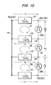
- Fig. 19 illustrates a sixth embodiment of the present invention, in which switching elements 25a and 25b are connected in series to the respective winding ends of the primary winding 27 and are controlled by the drive circuit 38 to be turned ON and OFF at the same timing.
- the other ends of the switching elements 25a and 25b are connected to the respective ends of the input capacitor 37.
- the electrostatic shield layer 46 which is connected to the winding end 32 which is the static end of the secondary winding 28.
- the output terminal 19a is also a static end and, therefore, even if the electrostatic shield layer 46 is connected to the output terminal 19b, the same effect is obtained.
- the other reference numerals and characters are the same as those in Fig. 3.
- Such an arrangement as mentioned above produces the effect of reducing the switching voltage which is developed between the input and output terminals 18a and 19a, that is, the common mode switching noise.
- the switching voltage e 2 which is induced across the second winding 28 is not generated as a voltage (the common mode switching noise) between the input and output terminals 18a and 19a because the electrostatic shield layer 46 is interposed between the primary and secondary windings 27 and 28 and is connected to the winding end 32 which is the static end of the secondary winding 28.
- switching voltages yielded between the electrostatic shield 46 and the winding end 29 (or 31) and between the winding end 29 (or 31) and the input terminal 18a (or 18b) which are the both ends of the switching element 25a (or 25b) become opposite in polarity and they are cancelled each other, so that the switching voltage e 1 produced across the primary winding 27 is not developed as a voltage (the common switching noise) between the input and output terminals 18a and 19a.
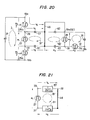
- Fig. 20 shows the common mode switching noise reducing action in the DC-DC converter of Fig. 19 in respect of the AC components of the noise.
- Fig. 20 the same characters as those in Fig. 19 are used, e 1 , e 2 , v 4 and v 5 each indicate a switching voltage between terminals at a given time point and the arrows show the interrelation of the polarities of the voltages.
- the parts corresponding to those in Fig. 17 are identified by the same reference numerals and the closed circuits III and VIII are identical with those in Fig. 17.
- the closed circuit I is formed by the capacitor 37, the primary winding 27 and the switching elements 25a and 25b, and the closed circuit IV' is formed by the primary winding 27, the capacitors 57 and 61 and the electrostatic shield layer 46.
- the input capacitor 37 shows a short with respect to the switching frequency component, and hence does not induce thereacross any switching voltage.
- the switching voltage e 1 Across the primary winding 27 is induced the switching voltage e 1 .
- the switching elements 25a and 25b are turned ON and OFF in in-phase relation. Accordingly, a switching voltage which is opposite in polarity to the switching voltage e 1 induced across the primary winding 27 and the amplitude of which is one-half of the amplitude of the voltage e 1 is developed across each of the switching elements 25a and 25b through the Kirchhoff's voltage law in the closed circuit I.
- the amplitudes of the switching voltages across the switching elements 25a and 25b are represented by e 1/ 2 + ⁇ and e 1/ 2 - A, respectively.
- the capacitors 57 and 61 each indicate in the form of a lumped parameter approximation of the stray capacitance distributed between the electrostatic shield layer 46 and the primary winding 27.
- the capacitor 57 is connected between the electrostatic shield layer 46 and the winding end 29, and the capacitor 61 is connected between the electrostatic shield layer 46 and the winding end 31.
- the capacitors 57 and 61 are both small in capacitance value and exhibit sufficiently high impedances over the high-frequency range including the switching frequency.
- Fig. 21 is an enlarged view showing of the closed circuit IV'.
- the same reference characters as those in Fig. 20 are used and the capacitance values of the capacitors 57 and 61 are represented by C 5 and C 6 , respectively.. Solving an equation in connection with the closed circuit IV' of Fig. 21, it follows that
- the common mode switching voltage is the switching voltage which is generated between the input and output terminals 18a and 19a and, letting this voltage be represented by v 6 , it follows from Fig. 20 that
- Figs. 16 and 19 the present invention has been described as being applied to what is called ON-OFF type DC-DC converter in which the half-wave rectifying diode 34 on the output side is conducted when the switching elements 25, 25a and 25b on the input side are in the OFF state
- the methods employed in Figs. 16 and 19 are also be applicable to what is called ON-ON type DC-DC converter in which the half-wave rectifying diode on the output side is conducted when the switching elements on the input side are in the ON state.
- Fig. 22 shows its example corresponding to Fig. 16. The difference between these circuit arrangements is that the polarity of the half-wave rectifying diode 34 in Fig. 22 is reverse from that in the case of Fig. 16.
- Fig. 23 illustrates the ON-ON type DC-DC converter corresponding to the converter of Fig. 19 and, in this case, too, the former differs from the latter only in the polarity of the half-wave rectifying diode 34.
- Fig. 24 illustrates a ninth embodiment of the present invention.
- an electrostatic shield layer 46p is interposed between the primary and secondary windings 27 and 28 and is connected to the static end of the primary winding 27, for instance, the winding end 29.
- another electrostatic shield layer 46s is interposed between the electrostatic shield layer 46p and the secondary winding 28 and is connected to the static end of the secondary winding 28, for example, the winding end 32.
- the electrostatic shield layers 46p and 46s are electrically separated from each other by an insulating film.
- Reference numerals and characters used in Fig. 24 are the same as those in Fig. 3.
- Fig. 25 shows an equivalent circuit of the DC-DC converter in terms of AC components in noise.
- the input side on the side of the electrostatic shield layer 46p is identical with the input side on the side of the electrostatic shield layer 46 in Fig. 9, so that the switching voltage e 1 generated on the input side is confined thereto by the electrostatic shield layer 46p, exerting no influence on the voltage between the input and output terminals 18a and 19a.
- the output side on the side of the electrostatic shield layer 46s is identical with the output side on the side of the electrostatic shield layer 46 in Fig. 17, so that the switching voltage e 2 generated on the output side is confined thereto by the electrostatic shield 46s, exerting no influence on the voltage between the input and output terminals 18a and 19a.
- the DC-DC converter of Fig. 24 is free from the generation of the switching voltage between the input and output terminals 18a and 19a. It is evident that the method of providing the two electrostatic shield layers 46p and 46s is also applicable to the ON-ON type DC-DC converter.
- the input and output side of the DC-DC converter can be isolated by a high impedance over a high-frequency range including DC and the switching frequency and the generation of the common mode switching noise can be suppressed.
- the DC-DC converter of the present invention is suitable for use, for example, as the power receiving source 17 for the digital line terminating equipment which is installed in the subscriber's premises and activated by remote power feeding from the central office and as the power feeding source 5 of the central office in the digital subscriber line transmission system using the balanced type cable, described previously in respect of Fig. 1.
- the present invention prevents that the switching noise developed by the DC-DC converter is induced in the pulse transmission system, permitting that the digital line terminating equipment and the subscriber's line can be isolated by a high impedance. This ensures to provide a high common mode rejection ratio of the digital line terminating equipment in the pulse transmission band, minimizing the occurrence of a code error of the digital signal with respect to large common mode noise that is induced on the subscriber's line.
Landscapes
- Engineering & Computer Science (AREA)
- Power Engineering (AREA)
- Dc-Dc Converters (AREA)
Applications Claiming Priority (4)
| Application Number | Priority Date | Filing Date | Title |
|---|---|---|---|
| JP13236582A JPS5925579A (ja) | 1982-07-28 | 1982-07-28 | Dc−dc変換回路 |
| JP132364/82 | 1982-07-28 | ||
| JP132365/82 | 1982-07-28 | ||
| JP13236482A JPS5925578A (ja) | 1982-07-28 | 1982-07-28 | Dc−dc変換回路 |
Publications (3)
| Publication Number | Publication Date |
|---|---|
| EP0100098A2 true EP0100098A2 (de) | 1984-02-08 |
| EP0100098A3 EP0100098A3 (en) | 1985-12-11 |
| EP0100098B1 EP0100098B1 (de) | 1987-11-25 |
Family
ID=26466952
Family Applications (1)
| Application Number | Title | Priority Date | Filing Date |
|---|---|---|---|
| EP83107388A Expired EP0100098B1 (de) | 1982-07-28 | 1983-07-27 | Gleichstromumformer für Fernstromversorgung |
Country Status (3)
| Country | Link |
|---|---|
| US (1) | US4507721A (de) |
| EP (1) | EP0100098B1 (de) |
| DE (1) | DE3374745D1 (de) |
Cited By (5)
| Publication number | Priority date | Publication date | Assignee | Title |
|---|---|---|---|---|
| US4679132A (en) * | 1985-08-08 | 1987-07-07 | American Telephone And Telegraph Company, At&T Bell Laboratories | Floating battery feed circuit using multifilar transformer |
| US4780696A (en) * | 1985-08-08 | 1988-10-25 | American Telephone And Telegraph Company, At&T Bell Laboratories | Multifilar transformer apparatus and winding method |
| GB2254202A (en) * | 1991-03-19 | 1992-09-30 | Kijima Co Ltd | Electric converter |
| EP2184748A3 (de) * | 2008-11-06 | 2014-04-09 | Power Integrations, Inc. | Verfahren und Vorrichtung zur Einstellung des Verschiebungsstroms in einem Energieübertragungselement |
| US9356504B2 (en) | 2011-02-17 | 2016-05-31 | Salcomp Oyj | Power supply with interference suppression, and method for operating a power supply |
Families Citing this family (24)
| Publication number | Priority date | Publication date | Assignee | Title |
|---|---|---|---|---|
| JPH0521986Y2 (de) * | 1986-03-17 | 1993-06-04 | ||
| US4814965A (en) * | 1987-09-30 | 1989-03-21 | Spectra Physics | High power flyback, variable output voltage, variable input voltage, decoupled power supply |
| US5724236A (en) * | 1996-03-05 | 1998-03-03 | Motorola, Inc. | Power converter transformer having an auxilliary winding and electrostatic shield to suppress noise |
| US6480510B1 (en) | 1998-07-28 | 2002-11-12 | Serconet Ltd. | Local area network of serial intelligent cells |
| US6956826B1 (en) | 1999-07-07 | 2005-10-18 | Serconet Ltd. | Local area network for distributing data communication, sensing and control signals |
| US6690677B1 (en) | 1999-07-20 | 2004-02-10 | Serconet Ltd. | Network for telephony and data communication |
| US6549616B1 (en) | 2000-03-20 | 2003-04-15 | Serconet Ltd. | Telephone outlet for implementing a local area network over telephone lines and a local area network using such outlets |
| RU2168837C1 (ru) * | 2000-04-05 | 2001-06-10 | Открытое акционерное общество "Концерн Энергомера" | Сглаживающий фильтр |
| US6549431B2 (en) * | 2001-03-08 | 2003-04-15 | Power Integrations, Inc. | Method and apparatus for substantially reducing electrical earth displacement current flow generated by wound components |
| US6995990B2 (en) * | 2001-03-08 | 2006-02-07 | Power Integrations, Inc. | Method and apparatus for substantially reducing electrical earth displacement current flow generated by wound components |
| RU2214036C2 (ru) * | 2001-09-20 | 2003-10-10 | Открытое акционерное общество "Научно-исследовательский институт вычислительных комплексов им. М.А. Карцева" | Сетевой фильтр для оборудования, питающегося от сети переменного тока с заземленной нейтралью |
| IL154234A (en) | 2003-01-30 | 2010-12-30 | Mosaid Technologies Inc | Method and system for providing dc power on local telephone lines |
| IL159838A0 (en) | 2004-01-13 | 2004-06-20 | Yehuda Binder | Information device |
| US20070070911A1 (en) * | 2005-09-29 | 2007-03-29 | Goldberg Keith J | Method for testing links in a wireless network |
| TWI306327B (en) * | 2005-12-30 | 2009-02-11 | System General Corp | An energy transfer device for reducing a conductivity electromagnetic interference and manufacturing method thereof |
| TWI343586B (en) * | 2006-07-21 | 2011-06-11 | Delta Electronics Inc | Power source transforming device and transformer thereof |
| JP5434370B2 (ja) * | 2009-08-26 | 2014-03-05 | サンケン電気株式会社 | 共振型スイッチング電源装置 |
| WO2012064063A2 (ko) * | 2010-11-09 | 2012-05-18 | Park Chan-Woong | 전기적 잡음을 상쇄시키는 자기에너지전달소자 및 전원장치 |
| US8791687B2 (en) | 2012-05-24 | 2014-07-29 | Agilent Technologies, Inc. | Transformer correction circuit and technique for reducing cross-talk current |
| US9478351B2 (en) * | 2013-05-24 | 2016-10-25 | Keithley Instruments, Inc. | Isolation transformer for use in isolated DC-to-DC switching power supply |
| DE102013106702B4 (de) * | 2013-06-26 | 2017-08-31 | Sma Solar Technology Ag | Verfahren und Vorrichtung zum Erkennen eines Lichtbogens |
| CN103731011B (zh) * | 2013-12-31 | 2016-05-11 | 深圳航天科技创新研究院 | 一种用于公路远距离供电的高可靠恒流转恒压装置 |
| FR3029370A1 (fr) * | 2014-12-02 | 2016-06-03 | Orange | Procede et dispositif d'annulation de bruit pour les systemes de transmission bifilaires |
| US9722499B2 (en) * | 2015-12-08 | 2017-08-01 | Power Integrations, Inc. | Energy transfer element with capacitor compensated cancellation and balance shield windings |
Family Cites Families (9)
| Publication number | Priority date | Publication date | Assignee | Title |
|---|---|---|---|---|
| GB1449646A (en) * | 1972-11-20 | 1976-09-15 | Matsushita Electric Industrial Co Ltd | High voltage generator for television apparatus |
| DE2444894A1 (de) * | 1974-09-19 | 1976-04-08 | Siemens Ag | Transformator mit galvanischer trennung der primaer- und sekundaerseite |
| GB1539757A (en) * | 1975-06-11 | 1979-01-31 | Sony Corp | Transformers and converters including such transformers |
| JPS523132A (en) * | 1975-06-25 | 1977-01-11 | Nakamichi Corp | Power source device |
| JPS5625384A (en) * | 1979-08-09 | 1981-03-11 | Toshiba Corp | Self-excited converter |
| JPS5660004A (en) * | 1979-10-19 | 1981-05-23 | Sony Corp | Parts of insulated inductance |
| DE3001975A1 (de) * | 1980-01-21 | 1981-07-23 | Licentia Patent-Verwaltungs-Gmbh, 6000 Frankfurt | Zeilentransformator fuer einen fernsehempfaenger |
| JPS56148179A (en) * | 1980-04-21 | 1981-11-17 | Fujitsu Ltd | Converting method of ac-dc |
| US4443839A (en) * | 1980-12-23 | 1984-04-17 | Tokyo Shibaura Denki Kabushiki Kaisha | Single ended, separately driven, resonant DC-DC converter |
-
1983
- 1983-07-21 US US06/515,754 patent/US4507721A/en not_active Expired - Lifetime
- 1983-07-27 DE DE8383107388T patent/DE3374745D1/de not_active Expired
- 1983-07-27 EP EP83107388A patent/EP0100098B1/de not_active Expired
Cited By (6)
| Publication number | Priority date | Publication date | Assignee | Title |
|---|---|---|---|---|
| US4679132A (en) * | 1985-08-08 | 1987-07-07 | American Telephone And Telegraph Company, At&T Bell Laboratories | Floating battery feed circuit using multifilar transformer |
| US4780696A (en) * | 1985-08-08 | 1988-10-25 | American Telephone And Telegraph Company, At&T Bell Laboratories | Multifilar transformer apparatus and winding method |
| GB2254202A (en) * | 1991-03-19 | 1992-09-30 | Kijima Co Ltd | Electric converter |
| GB2254202B (en) * | 1991-03-19 | 1995-01-11 | Kijima Co Ltd | Electric converter |
| EP2184748A3 (de) * | 2008-11-06 | 2014-04-09 | Power Integrations, Inc. | Verfahren und Vorrichtung zur Einstellung des Verschiebungsstroms in einem Energieübertragungselement |
| US9356504B2 (en) | 2011-02-17 | 2016-05-31 | Salcomp Oyj | Power supply with interference suppression, and method for operating a power supply |
Also Published As
| Publication number | Publication date |
|---|---|
| EP0100098B1 (de) | 1987-11-25 |
| DE3374745D1 (en) | 1988-01-07 |
| EP0100098A3 (en) | 1985-12-11 |
| US4507721A (en) | 1985-03-26 |
Similar Documents
| Publication | Publication Date | Title |
|---|---|---|
| US4507721A (en) | DC-DC Converter for remote power feeding | |
| US12125631B2 (en) | Shielded electrical transformer | |
| US6693805B1 (en) | Ripple cancellation circuit for ultra-low-noise power supplies | |
| US8472215B2 (en) | Grid-tie inverter for interconnecting AC voltage to electric power grid | |
| US4667173A (en) | Line filter | |
| US4355352A (en) | DC to DC Converter | |
| FR2468193A1 (fr) | Transformateur notamment utilisable comme regulateur de commutation | |
| US7672147B1 (en) | High attenuation filtering circuit for power converters | |
| US4910653A (en) | Power converter with cascaded output transformers | |
| US4855891A (en) | Power supply design | |
| JPS59129571A (ja) | スイツチング電源 | |
| US4725936A (en) | High-voltage stabilizing power supply apparatus with an improved inductive noise compensation | |
| EP3928334A1 (de) | Gleichtaktdrossel | |
| US4011410A (en) | Communication system interface circuits | |
| US4767978A (en) | Hybrid switching circuit in a DC to DC converter | |
| JPH0745451A (ja) | スイッチングトランス | |
| JPH0463628B2 (de) | ||
| US5508673A (en) | High frequency transformer apparatus | |
| US4912447A (en) | Transformer with channels in bobbin | |
| JPH0113309B2 (de) | ||
| US6930894B2 (en) | Switching power supply and distributed parameter structure | |
| EP0400271A2 (de) | Hochspannungsgenerator-Einrichtung vom Typ eines in mehrfachen Stufen isolierenden Transformators | |
| JPH0530145B2 (de) | ||
| US4660134A (en) | DC-DC converter with chopping switch and transformer | |
| JP6828839B2 (ja) | スイッチング電源装置 |
Legal Events
| Date | Code | Title | Description |
|---|---|---|---|
| PUAI | Public reference made under article 153(3) epc to a published international application that has entered the european phase |
Free format text: ORIGINAL CODE: 0009012 |
|
| 17P | Request for examination filed |
Effective date: 19830727 |
|
| AK | Designated contracting states |
Designated state(s): DE FR GB SE |
|
| PUAL | Search report despatched |
Free format text: ORIGINAL CODE: 0009013 |
|
| RAP1 | Party data changed (applicant data changed or rights of an application transferred) |
Owner name: NIPPON TELEGRAPH AND TELEPHONE CORPORATION |
|
| AK | Designated contracting states |
Designated state(s): DE FR GB SE |
|
| 17Q | First examination report despatched |
Effective date: 19861204 |
|
| GRAA | (expected) grant |
Free format text: ORIGINAL CODE: 0009210 |
|
| AK | Designated contracting states |
Kind code of ref document: B1 Designated state(s): DE FR GB SE |
|
| REF | Corresponds to: |
Ref document number: 3374745 Country of ref document: DE Date of ref document: 19880107 |
|
| ET | Fr: translation filed | ||
| PLBE | No opposition filed within time limit |
Free format text: ORIGINAL CODE: 0009261 |
|
| STAA | Information on the status of an ep patent application or granted ep patent |
Free format text: STATUS: NO OPPOSITION FILED WITHIN TIME LIMIT |
|
| 26N | No opposition filed | ||
| EAL | Se: european patent in force in sweden |
Ref document number: 83107388.7 |
|
| REG | Reference to a national code |
Ref country code: FR Ref legal event code: CA |
|
| REG | Reference to a national code |
Ref country code: GB Ref legal event code: IF02 |
|
| PGFP | Annual fee paid to national office [announced via postgrant information from national office to epo] |
Ref country code: SE Payment date: 20020531 Year of fee payment: 20 |
|
| PGFP | Annual fee paid to national office [announced via postgrant information from national office to epo] |
Ref country code: FR Payment date: 20020620 Year of fee payment: 20 |
|
| PGFP | Annual fee paid to national office [announced via postgrant information from national office to epo] |
Ref country code: GB Payment date: 20020724 Year of fee payment: 20 |
|
| PGFP | Annual fee paid to national office [announced via postgrant information from national office to epo] |
Ref country code: DE Payment date: 20020731 Year of fee payment: 20 |
|
| PG25 | Lapsed in a contracting state [announced via postgrant information from national office to epo] |
Ref country code: GB Free format text: LAPSE BECAUSE OF EXPIRATION OF PROTECTION Effective date: 20030726 |
|
| REG | Reference to a national code |
Ref country code: GB Ref legal event code: PE20 |
|
| EUG | Se: european patent has lapsed |