EP0100103A1 - Modulateur de largeur d'impulsions et circuit d'intégration pour former un produit analogue avec un tel modulateur de largeur d'impulsions - Google Patents
Modulateur de largeur d'impulsions et circuit d'intégration pour former un produit analogue avec un tel modulateur de largeur d'impulsions Download PDFInfo
- Publication number
- EP0100103A1 EP0100103A1 EP83107412A EP83107412A EP0100103A1 EP 0100103 A1 EP0100103 A1 EP 0100103A1 EP 83107412 A EP83107412 A EP 83107412A EP 83107412 A EP83107412 A EP 83107412A EP 0100103 A1 EP0100103 A1 EP 0100103A1
- Authority
- EP
- European Patent Office
- Prior art keywords
- signal
- pulse width
- triangular wave
- inversion
- width modulation
- Prior art date
- Legal status (The legal status is an assumption and is not a legal conclusion. Google has not performed a legal analysis and makes no representation as to the accuracy of the status listed.)
- Granted
Links
- 230000010354 integration Effects 0.000 title claims abstract description 21
- 238000001514 detection method Methods 0.000 claims description 2
- 230000007274 generation of a signal involved in cell-cell signaling Effects 0.000 claims 4
- 238000010586 diagram Methods 0.000 description 7
- 238000000034 method Methods 0.000 description 5
- 102100028043 Fibroblast growth factor 3 Human genes 0.000 description 3
- 102100024061 Integrator complex subunit 1 Human genes 0.000 description 3
- 101710092857 Integrator complex subunit 1 Proteins 0.000 description 3
- 108050002021 Integrator complex subunit 2 Proteins 0.000 description 3
- 239000000470 constituent Substances 0.000 description 2
Images


Classifications
-
- H—ELECTRICITY
- H03—ELECTRONIC CIRCUITRY
- H03M—CODING; DECODING; CODE CONVERSION IN GENERAL
- H03M1/00—Analogue/digital conversion; Digital/analogue conversion
- H03M1/66—Digital/analogue converters
- H03M1/82—Digital/analogue converters with intermediate conversion to time interval
-
- H—ELECTRICITY
- H03—ELECTRONIC CIRCUITRY
- H03K—PULSE TECHNIQUE
- H03K7/00—Modulating pulses with a continuously-variable modulating signal
- H03K7/08—Duration or width modulation ; Duty cycle modulation
Definitions
- This invention relates to a pulse width modulation circuit using a triangular wave generation circuit and to an integration circuit using the pulse width modulation circuit. More particularly, the present invention relates to an integration circuit which is particularly suitable for generating pulses in such a number as to be proportional to the integration of the product of two signals, and also to a pulse width modulation circuit used in the former.
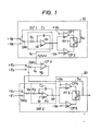
- Figure 1 illustrates a two-phase electronic type energy meter produced by modifying a three- phase electric energy meter disclosed on page 257 of INT. J. Electronics, 1980, Vol. 48, No. 3.
- a triangular wave generation circuit 10 consists of an integrator INT1 which selectively receives d.c. voltages V B and -V B via a switch SWl, a flip-flop FF1 generating a signal S ⁇ which controls the switch SW1 and first and second comparators CP1 and CP2 which control set and reset of the flip-flop, respectively.
- the integrator INT1 consists of a resistor Rl, a capacitance Cl and an amplifier Al.
- the comparators CP1 and CP2 compare the output of the amplifier Al with the reference voltages V R and -V R and generate signals for setting and resetting the flip-flop FF1 when they are in agreement, respectively.
- the switch SW1 changes over the voltage to V B and -V B when the signal S ⁇ is 0 and 1, respectively, and applies the voltage to the integrator INT1.
- the output signal V ⁇ from the circuit 10 becomes a triangular wave having an inclination of V B /(R 1 C 1 ) in both positive and negative and a peak of ⁇ V R .
- This output signal V ⁇ is applied to the non-inversion input terminal of the comparator CP3, and a first a.c. signal E V or its inversion signal -E V is applied as an input voltage V X to the inversion input terminal of the comparator CP3.
- the switch SW3 selects the signals -E V and E V when the later- appearing signal S V is 1 and 0, respectively.
- the output V of the comparator CP3 becomes "1" and "0" when the level difference between the triangular wave V ⁇ and the input voltage V x is positive and negative, respectively.
- the output signal V g becomes a signal formed by modulating the pulse width of the input signal V x .
- the degree of pulse modulation D is defined in the following manner: where a is the time in which V g is "1" during one cycle of V g (that is, one cycle of the triangular wave VA), and b is the time in which V is "0".
- the degree of pulse modulation D can be expressed as follows:
- the frequency of the triangular wave is selected to be sufficiently higher than the frequency of the signal S v and that of the signal E v .
- the signal V g modulated in this manner controls the selector switch SW2 for the second a.c. current E 1 proportional to a current applied to an electric system and its inversion signal -E i so that the switch SW2 selects the signals E i and -E i when the signal V g is 1 and 0, respectively.
- the mean value V M of the output V M of the switch SW2 over one cycle of the triangular wave is given as follows: .
- the mean value of V M with respect to time is proportional to the product of the first input V x and the second input E i .
- the selection output V M of the switch SW2 is applied to the integrator INT2 inside the pulse generation circuit 20.
- the integrator INT2 consists of a resistor R2, a capacitance C2 and an amplifier A2, and produces an integration signal V P of the input V M from the output terminal of the amplifier A2.
- Comparators CP4 and CP5 compare the integration signal V P with the reference voltages V R and -V R , respectively, and set and reset the flip-flop EF2 when they are in agreement, respectively.
- the integration value of the product of the voltage E v and the current E 1 can be measured by counting how many times the output S v of the flip-flop FF2 becomes 1.
- FIG. 2 is a circuit diagram showing the case in which these offset voltages are inserted as the equivalent voltage sources.
- the voltage sources F fA , V f1 - V f3 are those which equivalently express the offset quantities of the amplifier Al and comparators CP1 through CP3, respectively.
- the amplifier Al and the comparators CP1 - CP3 in Figure 2 can be regarded as having no offset.
- the triangular wave V ⁇ in this case has a waveform expressed by the following relation:'
- the mean voltage of this triangular wave V ⁇ becomes (V - V f1 ) and is not zero when the offset V f1 is not equal to the offset V f2 .
- this means voltage will be referred to as the "offset of the triangular wave”.
- this offset results from the difference of offset between the comparators CP1 and CP2.
- this triangular wave voltage V ⁇ appears as if it were shifted to a voltage VA'.
- the waveform of this voltage VA' has a value which is the sum of V f3 to the positive and negative turn-back voltages of the waveform of V ⁇ , respectively. The sum is more clearly illustrated in Figure 3.
- the degree of pulse width modulation D of the modulation signal V g is given by the following formula:
- the denominator of the second item is equivalent to the change of the reference voltage V R because of the existence of the offset voltages of the comparators CP1 and CP2.
- the influence resulting from the change of V R can be compensated for by such means as initial setting in the same way as the compensation of the deviation of the integration capacitance C2 and resistor R2 from the set values; hence, the influence is not hereby dealt with.
- V f is the sum of the offset of the triangular wave and the offset of the comparator CP3 but with a different polarity. Accordingly, this is referred to as an "overall offset”. If such an overall offset voltage exists, the mean value V M of V M in one cycle of the triangular wave, that corresponds to the formula (5), is given by the following formula:
- the frequency f 0 of the pulse S v becomes f «(V + V f ) x E.
- the overall offset voltage V f occurs as an error.
- This error depends upon the product of the overall offset V f and E i and hence, it is almost impossible to compensate for the error after detection of the pulse S . It is therefore necessary to cancel in advance the overall offset inside the pulse width modulation circuit.
- the present invention combines in principle means for cancelling the offset of a triangular wave by inverting either a triangular wave signal with respect to the input signal or the input signal with respect to the triangular wave signal every predetermined period, with means for eliminating the offset of comparators by inverting the output of the comparator, for replacing the input ter- minals of the comparators if the input signal is not inverted, and if the input signal is inverted, for connecting the input terminals of the comparator as such.
- a pulse width modulation circuit is constituted which comprises means for inverting the input signal and applying it to the same terminal of a comparator and means for inverting the output of the comparator, or a pulse width modulation circuit is constituted which comprises means for inverting a triangular wave signal and connecting the triangular wave signal and the input signal in an opposite manner to the inputs of the comparator and means for inverting the output of the comparator.
- a pulse width modulation circuit is provided which can simultaneously eliminate both of the offset of the triangular wave and the offset of the comparator.
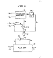
- the EOR gate L2 is disposed in order to eliminate the mean error, with respect to time, of the degree of pulse width modulation, as will be described elsewhere. It inverts the signal V g ' when the signal S ⁇ is 1.
- the EOR gate Ll inverts the output V g ' of the EOR gate L2 when the output pulse S v of the pulse generator 20 is 1, and the output S I of this EOR gate Ll is applied in place of the signal V g of Figure 1 to the switch SW2 (shown in Figure 1) inside the pulse generation circuit 20.
- the duty of the width modulated pulse V g generated from the comparator CP3 can be determined on the basis of a triangular wave V ⁇ ' oscillating between two reference voltages V R ' and -V R ' that are obtained by gathering all the offset of the comparators CPl through CP3, as explained in con- junction with the formula (7) and also on the basis of an equivalent input voltage V X ' which is formed by adding the input voltage E x to the inversion input terminal of the comparator CP3 and the overall offset voltage V f .
- V X ' equivalent input voltage
- FIG. 5 is a timing chart showing the relation between various signals and the triangular wave VA'.
- the signal S changes from 0 to 1 or from 1 to 0 whenever the signal V ⁇ ' coincides with either of ⁇ V R '.
- the signal S T is formed by halving the frequency of the signal S ⁇ , it changes from 0 to 1 or from 1 to 0 whenever the signal VA' coincides with either one of ⁇ V R '.
- Figure 5 shows the case in which the level of the signal S T changes whenever the signal V ⁇ ' coincides with V R '.
- the input voltage V X becomes E V and -E V whenever the signal S T becomes 0 and 1, respec- tively.
- Figure 5 shows the case in which V f >0 for the signal V X '.
- the solid line represents the pulses whose width is modulated and which are produced from the comparator CP3 and from the EOR gate L2 with respect to the signal V x ', respectively.
- the signal V g becomes 1 during the first period I in which the signal V ⁇ ' exceeds the signal V X ' and the signal VA' then becomes equal to the signal V X '.
- the signal V g ' becomes 1 during the second period II in which the signal V g is 1 and the signal S T is 0, or during the third period III in which the signal V g is 0 and the signal S T is 1.
- the mean degree of pulse width modulation D in one cycle of S T or the two cycles of the triangular wave is given as follows:
- the output S V of the flip-flop FF2 is inverted whenever the signal V P obtained by integrating this V M becomes equal to either one of ⁇ V R in the same way as in the case shown in Figure 1. Accordingly, the frequency of the pulse S V is proportional to the integrated value of the product of the signals E V and E i . Thus, a pulse having a frequency proportional to the power can be obtained on the basis of the signal V M .
- the inversion signal S T is produced by halving the frequency of the output S ⁇ of the triangular wave generation circuit.
- This is the most simple and reliable method.
- a method which increases the frequency division ratio by some multiples and a method which divides the frequency on the non-multiple basis can be used, in principle, but these methods are not much advantageous because the time required for each cancelling becomes long. If cancelling is effected in a period shorter than the period of the triangular wave, a problem will occur that the cancelling effect drops if the difference of inclinations of the triangualr wave exists.
- this method may be employed depending upon the intended application.
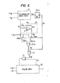
- FIG. 6 shows the second embodiment of the present invention, in which like reference numerals are used to identify like constituents as in Figure 4.
- This embodiment includes further acircuit 30 for generating a triangular wave signal -V which has the opposite polarity to the triangular wave signal V ⁇ by use of resistors R3 and R4 having the same value and an operational amplifier A3, and switches SW4 and SW5 for changing over +E v and ⁇ V by the output S T of the flip-flop FF3 and connecting them to the comparator CP3.
- the rest are the same as those of the circuit shown in Figure 4.
- the present invention can realize a voltage-frequency convertor which pro- vides a mean degree of pulse width modulation with respect to time, which is devoid of the influence of the triangular wave or comparator, with a high level of accuracy.
Landscapes
- Engineering & Computer Science (AREA)
- Theoretical Computer Science (AREA)
- Inverter Devices (AREA)
- Analogue/Digital Conversion (AREA)
- Amplifiers (AREA)
- Amplitude Modulation (AREA)
Applications Claiming Priority (2)
| Application Number | Priority Date | Filing Date | Title |
|---|---|---|---|
| JP57130336A JPS5922441A (ja) | 1982-07-28 | 1982-07-28 | デジタル出力型積分回路 |
| JP130336/82 | 1982-07-28 |
Publications (2)
| Publication Number | Publication Date |
|---|---|
| EP0100103A1 true EP0100103A1 (fr) | 1984-02-08 |
| EP0100103B1 EP0100103B1 (fr) | 1986-06-11 |
Family
ID=15031926
Family Applications (1)
| Application Number | Title | Priority Date | Filing Date |
|---|---|---|---|
| EP83107412A Expired EP0100103B1 (fr) | 1982-07-28 | 1983-07-27 | Modulateur de largeur d'impulsions et circuit d'intégration pour former un produit analogue avec un tel modulateur de largeur d'impulsions |
Country Status (5)
| Country | Link |
|---|---|
| US (1) | US4577154A (fr) |
| EP (1) | EP0100103B1 (fr) |
| JP (1) | JPS5922441A (fr) |
| KR (1) | KR910004638B1 (fr) |
| DE (1) | DE3364066D1 (fr) |
Cited By (5)
| Publication number | Priority date | Publication date | Assignee | Title |
|---|---|---|---|---|
| WO1986007509A1 (fr) * | 1985-06-05 | 1986-12-18 | Caterpillar Inc. | Convertisseur de signal analogique en coefficient d'utilisation |
| EP0352137A3 (en) * | 1988-07-22 | 1990-08-22 | Matsushita Electric Industrial Co., Ltd. | Pulse-width modulator and driving unit using the same |
| GB2279193A (en) * | 1993-06-16 | 1994-12-21 | Smiths Industries Plc | Pulse width modulators |
| RU2197059C2 (ru) * | 2000-06-16 | 2003-01-20 | Федеральное государственное унитарное предприятие "Научно-производственный центр "Полюс" | Блок периодической развертки для преобразователя напряжения с широтно-импульсной модуляцией |
| RU2254663C2 (ru) * | 2003-06-02 | 2005-06-20 | Федеральное государственное унитарное предприятие "Научно-производственный центр "Полюс" | Блок периодической развертки для следящего импульсного преобразователя |
Families Citing this family (9)
| Publication number | Priority date | Publication date | Assignee | Title |
|---|---|---|---|---|
| JPH088727B2 (ja) * | 1984-12-10 | 1996-01-29 | エヌティエヌ株式会社 | 磁気浮上式直線スライダ |
| US4816752A (en) * | 1988-04-07 | 1989-03-28 | Snap-On Tools Corporation | Method and apparatus for low power offset correction of amplified sensor signals |
| GB9417832D0 (en) * | 1994-09-05 | 1994-10-26 | Texas Instruments Ltd | A method and apparatus for processing an analogue signal |
| US6084450A (en) * | 1997-01-14 | 2000-07-04 | The Regents Of The University Of California | PWM controller with one cycle response |
| US6525842B1 (en) * | 1998-07-09 | 2003-02-25 | Canon Kabushiki Kaisha | Image processing apparatus and method of the same and storage medium |
| JP2001243715A (ja) * | 2000-02-24 | 2001-09-07 | Sony Corp | 波形整形回路 |
| US6381154B1 (en) * | 2001-03-16 | 2002-04-30 | Tranh To Nguyen | PWM nonlinear controller with a single cycle response and a non resettable integrator |
| KR100617960B1 (ko) * | 2005-02-24 | 2006-08-30 | 삼성전자주식회사 | 자가 발진형 펄스 폭 변조회로 및 펄스 폭 변조 방법 |
| KR102152530B1 (ko) * | 2019-04-08 | 2020-09-04 | 현대위아 주식회사 | 차량용 액슬 허브 씰링캡 |
Citations (2)
| Publication number | Priority date | Publication date | Assignee | Title |
|---|---|---|---|---|
| DE1512210B2 (de) * | 1966-02-10 | 1977-06-30 | Harris-Intertype Corp., Wilmington, Del. (V-StA.) | Pulsdauermodulator |
| GB1560350A (en) * | 1977-06-09 | 1980-02-06 | Communications Patents Ltd | Pulse-width modulators |
Family Cites Families (2)
| Publication number | Priority date | Publication date | Assignee | Title |
|---|---|---|---|---|
| US4066959A (en) * | 1976-12-29 | 1978-01-03 | General Electric Company | Electronic volt-square-hour metering method and apparatus |
| US4495463A (en) * | 1982-02-24 | 1985-01-22 | General Electric Company | Electronic watt and/or watthour measuring circuit having active load terminated current sensor for sensing current and providing automatic zero-offset of current sensor DC offset error potentials |
-
1982
- 1982-07-28 JP JP57130336A patent/JPS5922441A/ja active Granted
-
1983
- 1983-07-26 US US06/517,407 patent/US4577154A/en not_active Expired - Lifetime
- 1983-07-27 EP EP83107412A patent/EP0100103B1/fr not_active Expired
- 1983-07-27 DE DE8383107412T patent/DE3364066D1/de not_active Expired
- 1983-07-27 KR KR1019830003497A patent/KR910004638B1/ko not_active Expired
Patent Citations (2)
| Publication number | Priority date | Publication date | Assignee | Title |
|---|---|---|---|---|
| DE1512210B2 (de) * | 1966-02-10 | 1977-06-30 | Harris-Intertype Corp., Wilmington, Del. (V-StA.) | Pulsdauermodulator |
| GB1560350A (en) * | 1977-06-09 | 1980-02-06 | Communications Patents Ltd | Pulse-width modulators |
Cited By (7)
| Publication number | Priority date | Publication date | Assignee | Title |
|---|---|---|---|---|
| WO1986007509A1 (fr) * | 1985-06-05 | 1986-12-18 | Caterpillar Inc. | Convertisseur de signal analogique en coefficient d'utilisation |
| EP0352137A3 (en) * | 1988-07-22 | 1990-08-22 | Matsushita Electric Industrial Co., Ltd. | Pulse-width modulator and driving unit using the same |
| US5030847A (en) * | 1988-07-22 | 1991-07-09 | Rohm Co., Ltd. | Pulse-width modulator and driving circuit |
| GB2279193A (en) * | 1993-06-16 | 1994-12-21 | Smiths Industries Plc | Pulse width modulators |
| GB2279193B (en) * | 1993-06-16 | 1997-12-17 | Smiths Industries Plc | Signal processing |
| RU2197059C2 (ru) * | 2000-06-16 | 2003-01-20 | Федеральное государственное унитарное предприятие "Научно-производственный центр "Полюс" | Блок периодической развертки для преобразователя напряжения с широтно-импульсной модуляцией |
| RU2254663C2 (ru) * | 2003-06-02 | 2005-06-20 | Федеральное государственное унитарное предприятие "Научно-производственный центр "Полюс" | Блок периодической развертки для следящего импульсного преобразователя |
Also Published As
| Publication number | Publication date |
|---|---|
| JPH0468814B2 (fr) | 1992-11-04 |
| KR840005626A (ko) | 1984-11-14 |
| JPS5922441A (ja) | 1984-02-04 |
| KR910004638B1 (ko) | 1991-07-08 |
| EP0100103B1 (fr) | 1986-06-11 |
| US4577154A (en) | 1986-03-18 |
| DE3364066D1 (en) | 1986-07-17 |
Similar Documents
| Publication | Publication Date | Title |
|---|---|---|
| EP0100103A1 (fr) | Modulateur de largeur d'impulsions et circuit d'intégration pour former un produit analogue avec un tel modulateur de largeur d'impulsions | |
| US4246497A (en) | Phase measuring circuit | |
| EP0613256B1 (fr) | Convertisseur analogique-numérique avec signal de tremblement modulé | |
| US4112428A (en) | Clocked precision integrating analog to digital converter system | |
| US4862382A (en) | Arrangement for processing the output signals of a resistance bridge | |
| US4926178A (en) | Delta modulator with integrator having positive feedback | |
| EP0104999B1 (fr) | Dispositif pour changer de gain, avec erreur diminuée, pour un wattmètre | |
| US4573037A (en) | Analog-to digital converter and method | |
| JP2918578B2 (ja) | デジタル復調器 | |
| GB1598781A (en) | Analogue-digital converter and conversion method | |
| US5126743A (en) | System and method for converting a DSB input signal to a frequency encoded output signal | |
| JPH0528923B2 (fr) | ||
| US4839788A (en) | Bipolar voltage to frequency converter | |
| EP0467509A2 (fr) | Convertisseur intégrant de tension en fréquence | |
| US4470019A (en) | Rate multiplier square root extractor with increased accuracy for transmitter applications | |
| JPS60100830A (ja) | デジタル・アナログ変換装置 | |
| GB2227381A (en) | Analogue to digital converters | |
| SU661375A1 (ru) | Цифровой интегрирующий измеритель отношени двух посто нных напр жений | |
| SU1083139A1 (ru) | Цифровой феррозондовый магнитометр со след щим уравновешиванием | |
| SU938163A1 (ru) | Детектор квазиравновеси | |
| SU1056151A1 (ru) | Калибратор напр жени | |
| SU1451863A1 (ru) | Преобразователь ток-частота с импульсной обратной св зью | |
| EP0709970A2 (fr) | Dispositif de correction de la composante continue dans un convertisseur analogique numérique | |
| SU1739199A1 (ru) | Устройство дл записи информации | |
| SU1003331A1 (ru) | Аналого-цифровой преобразователь |
Legal Events
| Date | Code | Title | Description |
|---|---|---|---|
| PUAI | Public reference made under article 153(3) epc to a published international application that has entered the european phase |
Free format text: ORIGINAL CODE: 0009012 |
|
| AK | Designated contracting states |
Designated state(s): DE FR GB IT |
|
| 17P | Request for examination filed |
Effective date: 19840224 |
|
| GRAA | (expected) grant |
Free format text: ORIGINAL CODE: 0009210 |
|
| AK | Designated contracting states |
Kind code of ref document: B1 Designated state(s): DE FR GB IT |
|
| REF | Corresponds to: |
Ref document number: 3364066 Country of ref document: DE Date of ref document: 19860717 |
|
| ET | Fr: translation filed | ||
| ITF | It: translation for a ep patent filed | ||
| PLBE | No opposition filed within time limit |
Free format text: ORIGINAL CODE: 0009261 |
|
| STAA | Information on the status of an ep patent application or granted ep patent |
Free format text: STATUS: NO OPPOSITION FILED WITHIN TIME LIMIT |
|
| 26N | No opposition filed | ||
| ITTA | It: last paid annual fee | ||
| ITPR | It: changes in ownership of a european patent |
Owner name: CAMBIO RAGIONE SOCIALE;HITACHI MICROCOMPUTER SYSTE |
|
| REG | Reference to a national code |
Ref country code: FR Ref legal event code: CD |
|
| PGFP | Annual fee paid to national office [announced via postgrant information from national office to epo] |
Ref country code: FR Payment date: 19980710 Year of fee payment: 16 |
|
| PGFP | Annual fee paid to national office [announced via postgrant information from national office to epo] |
Ref country code: GB Payment date: 19980717 Year of fee payment: 16 |
|
| PGFP | Annual fee paid to national office [announced via postgrant information from national office to epo] |
Ref country code: DE Payment date: 19980928 Year of fee payment: 16 |
|
| PG25 | Lapsed in a contracting state [announced via postgrant information from national office to epo] |
Ref country code: GB Free format text: LAPSE BECAUSE OF NON-PAYMENT OF DUE FEES Effective date: 19990727 |
|
| PG25 | Lapsed in a contracting state [announced via postgrant information from national office to epo] |
Ref country code: FR Free format text: THE PATENT HAS BEEN ANNULLED BY A DECISION OF A NATIONAL AUTHORITY Effective date: 19990731 |
|
| GBPC | Gb: european patent ceased through non-payment of renewal fee |
Effective date: 19990727 |
|
| PG25 | Lapsed in a contracting state [announced via postgrant information from national office to epo] |
Ref country code: DE Free format text: LAPSE BECAUSE OF NON-PAYMENT OF DUE FEES Effective date: 20000503 |
|
| REG | Reference to a national code |
Ref country code: FR Ref legal event code: ST |