EP0100242A2 - Système optique pour un laser - Google Patents
Système optique pour un laser Download PDFInfo
- Publication number
- EP0100242A2 EP0100242A2 EP83304369A EP83304369A EP0100242A2 EP 0100242 A2 EP0100242 A2 EP 0100242A2 EP 83304369 A EP83304369 A EP 83304369A EP 83304369 A EP83304369 A EP 83304369A EP 0100242 A2 EP0100242 A2 EP 0100242A2
- Authority
- EP
- European Patent Office
- Prior art keywords
- lens
- laser
- optical system
- pattern
- image plane
- Prior art date
- Legal status (The legal status is an assumption and is not a legal conclusion. Google has not performed a legal analysis and makes no representation as to the accuracy of the status listed.)
- Granted
Links
Images




Classifications
-
- G—PHYSICS
- G02—OPTICS
- G02B—OPTICAL ELEMENTS, SYSTEMS OR APPARATUS
- G02B27/00—Optical systems or apparatus not provided for by any of the groups G02B1/00 - G02B26/00, G02B30/00
- G02B27/09—Beam shaping, e.g. changing the cross-sectional area, not otherwise provided for
-
- G—PHYSICS
- G02—OPTICS
- G02B—OPTICAL ELEMENTS, SYSTEMS OR APPARATUS
- G02B19/00—Condensers, e.g. light collectors or similar non-imaging optics
- G02B19/0004—Condensers, e.g. light collectors or similar non-imaging optics characterised by the optical means employed
- G02B19/0009—Condensers, e.g. light collectors or similar non-imaging optics characterised by the optical means employed having refractive surfaces only
- G02B19/0014—Condensers, e.g. light collectors or similar non-imaging optics characterised by the optical means employed having refractive surfaces only at least one surface having optical power
-
- G—PHYSICS
- G02—OPTICS
- G02B—OPTICAL ELEMENTS, SYSTEMS OR APPARATUS
- G02B19/00—Condensers, e.g. light collectors or similar non-imaging optics
- G02B19/0033—Condensers, e.g. light collectors or similar non-imaging optics characterised by the use
- G02B19/0047—Condensers, e.g. light collectors or similar non-imaging optics characterised by the use for use with a light source
- G02B19/0052—Condensers, e.g. light collectors or similar non-imaging optics characterised by the use for use with a light source the light source comprising a laser diode
-
- G—PHYSICS
- G02—OPTICS
- G02B—OPTICAL ELEMENTS, SYSTEMS OR APPARATUS
- G02B27/00—Optical systems or apparatus not provided for by any of the groups G02B1/00 - G02B26/00, G02B30/00
- G02B27/09—Beam shaping, e.g. changing the cross-sectional area, not otherwise provided for
- G02B27/0938—Using specific optical elements
- G02B27/095—Refractive optical elements
- G02B27/0955—Lenses
- G02B27/0966—Cylindrical lenses
Definitions
- This invention relates to an optical system for providing beam collimation 0 or beam focusing from a multi-emitter or broad emitter semiconductor laser having a phase locked radiation pattern emitting from a common p-n planar junction.
- the beam emitted from a facet of the laser is usually focused to a small spot in order to meet the needs of various applications, such as optical disk storage and laser printing, by means of reimaging the laser near field pattern to the desired image plane.
- optical systems designed for beam forming, focusing or shaping are disclosed in U.S. Patents 4,203,652; 4,253,735 and 4,323,297.
- semiconductor lasers possess-different points of origin of divergence (also referred to as beam waist positions) as well as angles of divergence for radiation emitted from the laser facet in directions orthogonal to each other, i.e., in a vertical emission direction which is perpendicular to the p-n planar junction and in a lateral emission direction which is parallel to and along the p-n planar junction.
- the points of origin of divergence also vary relative to different kinds of laser geometry as illustrated in Figures 1 and 2 of the accompanying drawings.
- FIG 1 the radiation beam characteristics for an index guided laser are illustrated.
- An index guided laser depends on differences in the index of refraction of materials due to the structural geometry of the laser, e.g., nonplanar layers, channels, mesas, etc., to guide the propagating radiation.
- radiation in both the vertical and lateral emission direction of laser 10 has a point of origin of divergence or beam waist position 11 at the laser facet 14. This beam waist position 11 is called the near field of the laser.
- radiation in the vertical emission direction of laser 10 has a point of origin of divergence or beam waist position 11 at facet 14 at the point of emission from the laser optical cavity as represented by the p-n junction 15.
- radiation in the lateral emission direction of laser 10 has a point of origin of divergence or beam waist position 11 also at facet 14 at the point of emission from the laser optical cavity as represented by line 17, which line is illustrative of the laser stripe geometry.
- Spherical lens. 16 collimates beam 12 from laser 10 and spherical lens 18 focuses beam 12 to'a spot 20 onto image plane 22. Because the beam waists 11 in both the vertical and lateral directions lie at facet surface 14 in an index guided laser, the near field pattern of the laser can be imaged into a diffraction limited spot 20 at the image plane 22.
- a more difficult situation is present in gain guided lasers, illustrated in Figure 2 where the radiation beam characteristics are illustrated for such a laser.
- a gain guided laser depends on current dependent differences in the index of refraction of semiconductor materials comprising the structural layers of the laser to guide the propagating radiation.
- radiation in the vertical emission direction of laser 30 has a point of origin of divergence or beam waist position 31 at the laser facet 34 and at the p-n planar junction 35.
- Spherical iens 36 collimates beam 32 from laser 30 and spherical lens 38 focuses beam 32 to a spot 40 onto image plane 42.
- radiation in the lateral emission direction of laser 30 has a point of origin of divergence or beam waist position well within laser 30, e. g., 10 to 40 ⁇ m behind facet 34, as indicated at 39.
- the line 37 is illustrative of the laser stripe geometry and the position of the optical cavity of the laser. Because of this factor, the image plane for the beam in the lateral emission direction will not be in the same plane as the vertical emission direction if lens 37 is omitted. As a result, lens 36 will not be at the proper focal point. With the addition of the convex collimating lens 37, however, the near field pattern of the beam 32 can be collimated for focus by lens 38 to a spot 40 onto image plane 42.
- a still further improved monolithic multi-emitter laser device is disclosed in U.S. Patent 4,255,717 to Scifres et al.
- the power output of a recent multi-emitter semiconductor laser has been reported recently by Scifres et al at the Optical Fiber Conference in April, 1982 entitled, "Coupled Multiple Stripe Quantum Well Injection Lasers Emitting 400 mW CW".
- An optically coupled multiple stripe quantum well injection laser was disclosed which emitted up to a total of 400 mW of continuous output power with over 140 mW CW radiation being coupled into an optical fiber. At this writing, these CW power levels have well exceeded 500 mW.
- What is needed in this art is an optical system that makes it possible to combine the output power of the multi-emission or broad emission from such a laser to provide a single high power coherent and collimated beam which may be further focused to a single high power spot.
- an optical system for producing a single beam from a multi-emitter or broad emitter semiconductor laser comprising a broad phase coherent emission region in one direction and a very small radiation emitting region in the orthogonal direction.
- a broad phase coherent region would normally be fabricated from a common p-n planar junction, e.g., U.S. patent 4,255,717, although other broad phase coherent regions have also been disclosed and described in the art which do not have a common p-n planar junction, e.g., U.S. patent 4,280,108.
- the pattern from such a laser characteristically has one or more low angular divergence beams along the broad phase coherent emitter direction. These broad low divergence beams constitute the far field radiation pattern of the laser.
- An optical system must be provided to compensate for these differing orthogonal beams as well as provide a single focused spot from the multi-emitter or broad emitter laser source.
- first lens system to focus radiation in the near field pattern of radiation emitted from the laser in the small emission direction, normally the direction perpendicular to the p-n planar junction
- second lens system to focus radiation in the far field pattern of radiation emitted from the laser in the lateral emission direction, normally the direction parallel with and along the p-n planar junction, whereby a single collimated beam is produced from the laser output
- the lens system may also exclude means to focus the combined near and far field beams in these orthogonal directions resulting in a single collimated beam in both axes.
- the present invention is not limited to a multi-emitter laser but is also applicable to a broad emitter laser, i.e., any such - emitter capable of producing the phase coherence effect necessary across a broad facet region as at a common p-n junction of the laser.
- the highest power interference to be present in the pattern may be imaged and formed into a diffraction limited spot for desired beam spot modulated and scanning applications. Unwanted lower power interference lobes present in the far field pattern may be blocked by using an aperture in the optical system.
- the multi-emitter phase locked laser 70 has a p-n planar junction 75 and a beam waist position 71 at the plane of that junction located at the laser front facet 74.
- the laser 70 has a ten stripe contact geometry at 77, indicative that its emission in the lateral emission direction is ten spatially disposed emitters of radiation in the near field.. These ten emitters form a broad and fairly uniform intensity phase coherent ra diation emitting source.
- An example of the near field intensity profile as a function of spatial position for such a laser is illustrated in Figure 10.
- the phased laser 70 may be either of the index or gain guided type. This is because in the vertical emission direction of the laser illustrated in Figure 4A, imaging is being accomplished for the near field pattern of emission at the laser facet 74, in this case refocusing that pattern to a spot 80 at the image plane 82. However, in the lateral emission direction of the laser illustrated in Figure 4B, reimaging is being accomplished for the far field pattern of emission outside and beyond the laser facet 74 at a theoretical focal point at infinity. In this case, the far field pattern is focused to the spot 80 at the image plane 82.
- the far field pattern may provide one or more diffracted orders or interference lobes due to phased locked emission providing interference of radiation in the region between the near and far field
- the single principal diffracted order or interference " lobe may be formed into a collimated beam or onto an image plane, as illustrated in Figures 4A and 4B.
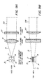
- the optical system of Figures 4A and 4B to focus the beam 72 in the vertical near field and in the lateral far field comprises lens system 76 and 78.
- cylinder lens 76 collimates the near field pattern and spherical lens 78 refocuses the collimated beam 72 at a spot 80 onto image plane 82.
- cylinder lens 76 has no optical effect but spherical lens 74 focuses the lateral far field pattern to the spot 80 at the image plane 82.
- the ability to refocus the lateral direction emission depends on the degree of coherence across the laser emission pattern.
- the correction required due to the finite divergence of the lateral far field beam 72', may be obtained by first, focusing the lateral far field beam 72' into a spot 80 on the image plane 82 by adjustment of the spherical lens 78 such that lens 78 lies at a distance L 2 which is slightly larger than the focal length f 2 of lens 78.
- cylinder lens 76 is adjusted so that it lies at a distance L l which is slightly smaller than the focal length f l of lens 76 to make the vertical near field of the beam 72 lie at the same spot 80 as the focus spot of the far field beam.
- This adjustment corresponds to changing the divergence angle of beam 72 to be that of this beam at position 72A in Figure 5A, the beam at 72A having the same divergence angle as beam 72' at this same point in Figure 5B thereby allowing imaging of both the vertical near Held spot at 71 and the lateral far field beam 72' onto a common image plane 82.
- Figure 6 illustrates another embodiment for reimaging the beam from the multi-emitter laser 70.
- the difference illustrated here relative to the previous embodiment lies in the manner of refocusing to an intermediate image plane at spot 80' and the use of an aperture 79 to block undesirable side or lower power interference lobes or diffraction orders that may be present in the far field pattern.
- the optical system of Figure 6 differs from previous embodiments in that, in the vertical emission direction illustrated in Figure 6A, the optical system for the near field pattern or beam waist position at 71 is focused onto image plane 82 by means of the cylinder lens 76 via the aperture 79.
- the optical system for the far field lateral pattern illustrated in Figure 6B is first focused to an image plane at the aperture 79 by means of the cylinder lens 75. Focusing to the aperture 79 in the lateral emission direction forms an apertured spot 80' which, with cylinder lens 81 with a properly selected focal length, reimages spot 80' to spot 80 at the image plane 82.
- the optical system of Figure 7 is similar to the optical system of Figure 4 but differs in that reimaging in the lateral emission direction is accomplished initially for reimaging to the image plane in a manner somewhat similar to Figure 6B.
- the near field spot 71 emission is collimated by spherical lens 75' and the collimated beam 72A is refocused to spot 80 at the image plane 82 by means of spherical lens 78.
- Spot 80 in Figure 7A therefore, is an image of the near field spot at 71.
- the same spherical lens 75' reimages the far field pattern 72' to a spot 80' at aperture 79.
- Spot 80' is then reimaged by cylinder lens 76' to a collimated beam 72A', which is refocused to spot 80 in the image plane 82 by spherical lens 78.
- aperture 79 is not necessary if a single low divergence far field lobe, vis a vis a multiple far field lobe pattern, is emitted by the laser since only a single spot will be formed at the image plane 82 under these conditions. Also, it should be noted that other apertures may be positioned at other locations in the optical path, such as illustrated'at 79' in Figures 7A and 7B, in order to select a single radiation beam angle.
- Figures 8A & B and Figures 9A & B are basically the embodiments respectively shown in Figures 7A & 7B and Figures 5A & 5B but absent the spherical lens 78 for refocusing the collimated beam 72 to a spot 80.
- the cylinder lens 75' collimates the vertical near field emission while focusing the lateral far field emission to spot 80'.
- Cylinder lens 76' reimages the vertical and lateral beam 72 to collimation, forming the orthogonal collimated beam 72B.
- the cylinder lens 76 collimates the vertical near field emission while the cylinder lens 76" collimates the lateral far field emission forming the orthogonal collimated beam 72B.
- the laser employed comprised a multi-emitter semiconductor laser 70 having ten phase locked emitters, as represented at 77 in Figure 7B, capable of emitting up to about 200 mW of CW output power (approximately 200 mW per laser facet) at 770mm. T he external differential quantum efficiency from both facets was about 65%.
- Laser 70 consisted of 10 parallel proton implanted three mm wide stripe geometry lasers on 10 micron centers on a single semiconductor substrate of n-type GaAs. There are no direct couplers between the stripes along the length of the laser as disclosed in U.S. Patent 4,255,717.
- phase locking is achieved by overlapping wave coupling due to the close proximity of adjacent laser cavities, as found in the structure disclosed in the Scifres et al article entitled “Phase-Locked Semioconductor Laser Array", supra.
- the active region of the laser consisted of a single 60 mm thick layer of undoped Ga 0.85 Al 0.15 As.
- the p- and n-type cladding layers were composed of Ga 0.35 Al 0.65 As and were 2.5 microns thick.
- a 0.6 micron thick p+ GaAs cap layer was used to obtain good ohmic contact
- Buffer layers approximately 0.5 mm thick and composed of Ga 0.8 Al 0.2 As were fabricated between the substrate and the n-type cladding layer and between the p-type cladding layer and the p+ GaAs cap.
- the laser chips were cleaved to a length of 250 mm and were mounted p-side down with Indium solder. The lasers were operated under both pulsed (300 nsec pulse width, 5 kHz repetition rate) and CW conditions.
- the radiation was collected by the high numerical aperture microscope lens 75', specifically a 40 x, 0.65 N.A. objective.
- the vertical near field emission was collimated by the objective lens 75' while the lateral far field emission was focused behind the objective to spot 80'.
- the laser beam is highly collimated in the lateral direction, it still diverges slightly, as previously mentioned, due to diffraction, causing the far field focus point to occur at a distance slightly beyond the focal length of lens 75'.
- Cylinder lens 76' had a 333 mm focal length and was used to collimate the light emerging from the focused far field spot 80'. This collimated beam is then focused by the lens 78, specifically a 20 x, 0.4 N.A. objective, to the spot 80 on image plane 82.
- phase locked lasers may emit some power into other lateral directions, it may be desirable to use the slit aperture 79 at the lateral far field focal point to eliminate all but the primary lateral far field interference lobe.
- the slit aperture 79 at the lateral far field focal point to eliminate all but the primary lateral far field interference lobe.
- the current level employed laser operation was 400 mA and the output power per facet was at 110 mW.
- 60-70% of the optical power is concentrated in a single low divergence interference lobe at an angle of about minus 4° from the facet normal.
- the emission at an angle of about 4° from the facet normal is due to the fact that there is a non-zero phase shift between the laser emitters.
- the half width of the far field pattern is about 1.3°. This is to be compared to the theoretical divergence limit from a uniformly illuminated 93 Jl m wide aperture which would be about 0.5°.
- the laser 70 was aligned in the optical system shown in Figure 7. Shown in Figure 11 is the pulsed optical output vs. current curves 90 and 92, repsectively, for the output at the front facet 74 of the laser and for the output at the image plane 82.
- the laser threshold is about 200 mA, corresponding to a threshold current density of 800 A/cm 2 .
- the output vs. current curve 90 at the facet is linear to over 200 mW.
- the laser threshold is about 210 mA and the device fails catastrophically at a CW output of 210 mW from an unprotected or uncoated facet
- the output vs. current curve 92 at the image plane is also linear indicating that the laser mode pattern is stable with increasing current Approximately 60% of the optical power emitted from the laser facet is transferred to the image plane 82 by the optical system.
- Focused spots produceable at the image plane 82 by the optical system of Figure 7 are shown in Figure 12, along with corresponding lateral intensity scan lines indicative of output power intensity.
- Figure 12A shows imaged spots 94 and 96 when the optical power at the image plane 82 is measured at' about 11 mW. In this case, no aperture 79 was employed to eliminate lower power far field lobes 96 emitted at angles other than the primary lobe. The primary lobe at about minus 4° can be seen imaged at spot 94.
- Figure 12B shows an unapertured image with 110 mW at the image plane 82. As shown by the lateral intensity scan lines, about 70% of the power lies in the dominant imaged spot 94 while other power is emitted at different far field and larger angles indicated at 96.
- Figure 12C shows apertured image with aperture 79 placed in the optical system as illustrated in Figure 7.
- a uniform spot 98 of about 2.5 ⁇ m diameter and containing 50 mW of output power was formed.
- the half width of the spot 98 based on an intensity scan is about 2.0 ⁇ m, which is near the diffraction limit (approximately 1.9 ⁇ m) of the 20 x, 0.4 N.A. focusing objective lens 78.
- Optics employed were ordinary microscope objectives which were not antireflection coated for infrared emission from the laser 70.
- a phase-locked multi-emitter laser can emit over 150,mW of output power into a single stable low divergence lateral beam.
- this type of laser can be collimated and brought to focus in a single spot, thus allowing these high power semiconductor devices to be used in higher power applications, such as laser printing and optical recording.
- phase coherent broad emitter lasers with fairly uniform emission intensity across a broad lateral region of the laser facet may be focused to a spot using the optical system of this invention.
Landscapes
- Physics & Mathematics (AREA)
- General Physics & Mathematics (AREA)
- Optics & Photonics (AREA)
- Semiconductor Lasers (AREA)
- Glass Compositions (AREA)
- Gyroscopes (AREA)
Applications Claiming Priority (2)
| Application Number | Priority Date | Filing Date | Title |
|---|---|---|---|
| US40269582A | 1982-07-28 | 1982-07-28 | |
| US402695 | 1982-07-28 |
Publications (3)
| Publication Number | Publication Date |
|---|---|
| EP0100242A2 true EP0100242A2 (fr) | 1984-02-08 |
| EP0100242A3 EP0100242A3 (en) | 1986-02-19 |
| EP0100242B1 EP0100242B1 (fr) | 1989-11-29 |
Family
ID=23592974
Family Applications (1)
| Application Number | Title | Priority Date | Filing Date |
|---|---|---|---|
| EP19830304369 Expired EP0100242B1 (fr) | 1982-07-28 | 1983-07-28 | Système optique pour un laser |
Country Status (4)
| Country | Link |
|---|---|
| EP (1) | EP0100242B1 (fr) |
| JP (1) | JPS5933420A (fr) |
| CA (1) | CA1208466A (fr) |
| DE (1) | DE3380905D1 (fr) |
Cited By (16)
| Publication number | Priority date | Publication date | Assignee | Title |
|---|---|---|---|---|
| DE3636336A1 (de) * | 1985-10-25 | 1987-04-30 | Hitachi Ltd | Halbleiterlaser-vorrichtung mit phasengesteuerter anordnung |
| EP0272325A4 (fr) * | 1986-06-30 | 1988-06-27 | Medical Laser Res Co Ltd | Appareil therapeutique a laser a semiconducteur. |
| EP0310711A1 (fr) * | 1987-10-05 | 1989-04-12 | Hitachi, Ltd. | Dispositif optique avec une barrette de diode laser verrouillée en phase |
| EP0312652A1 (fr) * | 1987-10-19 | 1989-04-26 | Hitachi, Ltd. | Dispositif optique avec une barrette de diode laser verrouillée en phase |
| EP0269122A3 (en) * | 1986-11-28 | 1989-05-24 | Fuji Photo Film Co., Ltd. | Laser optical system |
| WO1989009980A1 (fr) * | 1988-04-14 | 1989-10-19 | Eastman Kodak Company | Systeme optique de transfert d'images ou de representations pour appareil de transfert thermique de colorants |
| FR2661008A1 (fr) * | 1990-04-12 | 1991-10-18 | Nidek Kk | Systeme de lentilles pour focaliser le faisceau de sortie d'un laser a semi-conducteur. |
| EP0298490A3 (fr) * | 1987-07-08 | 1991-11-21 | Fuji Photo Film Co., Ltd. | Système optique de laser semi-conducteur |
| US5319528A (en) * | 1990-08-01 | 1994-06-07 | Diomed Limited | High power light source |
| DE19520187C1 (de) * | 1995-06-01 | 1996-09-12 | Microlas Lasersystem Gmbh | Optik zum Herstellen einer scharfen Beleuchtungslinie aus einem Laserstrahl |
| DE19619481C1 (de) * | 1996-05-14 | 1997-11-27 | Aesculap Meditec Gmbh | Verfahren und Vorrichtung zum Abtragen von Material mit einem Laserstrahl |
| EP0864892A3 (fr) * | 1997-03-13 | 2000-08-23 | Robert Bosch Gmbh | Système de lentilles pour l'accouplage d'un laser à sémiconducteur à une fibre optique |
| EP1514633A2 (fr) | 1997-10-22 | 2005-03-16 | Carl Zeiss Meditec AG | Dispositif de formage d'objets |
| CN111992873A (zh) * | 2014-11-19 | 2020-11-27 | 通快激光与系统工程有限公司 | 用于射束成形的光学系统 |
| CN112666196A (zh) * | 2019-10-16 | 2021-04-16 | 北航(四川)西部国际创新港科技有限公司 | 一种射线整合装置 |
| CN116050091A (zh) * | 2022-12-21 | 2023-05-02 | 北京理工大学 | 一种脉冲激光引信探测器发射模块数字化预测系统及方法 |
Families Citing this family (2)
| Publication number | Priority date | Publication date | Assignee | Title |
|---|---|---|---|---|
| JPS60229007A (ja) * | 1984-04-27 | 1985-11-14 | Matsushita Electric Ind Co Ltd | 非等方的光スポツト形成方法 |
| RU2101743C1 (ru) * | 1995-01-12 | 1998-01-10 | Конструкторское бюро приборостроения | Коллимирующая оптическая система для полупроводникового лазера |
Family Cites Families (7)
| Publication number | Priority date | Publication date | Assignee | Title |
|---|---|---|---|---|
| JPS5390957A (en) * | 1977-01-20 | 1978-08-10 | Matsushita Electric Ind Co Ltd | Photo signal generator |
| US4318594A (en) * | 1977-02-15 | 1982-03-09 | Canon Kabushiki Kaisha | Beam shaping optical system |
| JPS54143659A (en) * | 1978-04-28 | 1979-11-09 | Canon Inc | Image forming optical system for semiconductor laser |
| JPS55108612A (en) * | 1979-02-13 | 1980-08-21 | Matsushita Electric Ind Co Ltd | Aperture optical device of semiconductor laser light |
| JPS55146633A (en) * | 1979-05-01 | 1980-11-15 | Victor Co Of Japan Ltd | Optical recording method |
| JPS56140768A (en) * | 1980-04-01 | 1981-11-04 | Matsushita Electric Ind Co Ltd | Optical device for multibeam scanning |
| JPS56163533A (en) * | 1980-05-19 | 1981-12-16 | Matsushita Electric Ind Co Ltd | Optical recorder and reproducer |
-
1983
- 1983-05-31 CA CA000429259A patent/CA1208466A/fr not_active Expired
- 1983-07-21 JP JP13203883A patent/JPS5933420A/ja active Pending
- 1983-07-28 DE DE8383304369T patent/DE3380905D1/de not_active Expired - Lifetime
- 1983-07-28 EP EP19830304369 patent/EP0100242B1/fr not_active Expired
Cited By (25)
| Publication number | Priority date | Publication date | Assignee | Title |
|---|---|---|---|---|
| DE3636336A1 (de) * | 1985-10-25 | 1987-04-30 | Hitachi Ltd | Halbleiterlaser-vorrichtung mit phasengesteuerter anordnung |
| GB2182168A (en) * | 1985-10-25 | 1987-05-07 | Hitachi Ltd | Phased-array semiconductor laser apparatus |
| US4791650A (en) * | 1985-10-25 | 1988-12-13 | Hitachi, Ltd. | Phased-array semiconductor laser apparatus |
| GB2182168B (en) * | 1985-10-25 | 1989-10-25 | Hitachi Ltd | Phased-array semiconductor laser apparatus |
| EP0272325A4 (fr) * | 1986-06-30 | 1988-06-27 | Medical Laser Res Co Ltd | Appareil therapeutique a laser a semiconducteur. |
| EP0269122A3 (en) * | 1986-11-28 | 1989-05-24 | Fuji Photo Film Co., Ltd. | Laser optical system |
| EP0298490A3 (fr) * | 1987-07-08 | 1991-11-21 | Fuji Photo Film Co., Ltd. | Système optique de laser semi-conducteur |
| EP0310711A1 (fr) * | 1987-10-05 | 1989-04-12 | Hitachi, Ltd. | Dispositif optique avec une barrette de diode laser verrouillée en phase |
| EP0312652A1 (fr) * | 1987-10-19 | 1989-04-26 | Hitachi, Ltd. | Dispositif optique avec une barrette de diode laser verrouillée en phase |
| WO1989009980A1 (fr) * | 1988-04-14 | 1989-10-19 | Eastman Kodak Company | Systeme optique de transfert d'images ou de representations pour appareil de transfert thermique de colorants |
| FR2661008A1 (fr) * | 1990-04-12 | 1991-10-18 | Nidek Kk | Systeme de lentilles pour focaliser le faisceau de sortie d'un laser a semi-conducteur. |
| US5463534A (en) * | 1990-08-01 | 1995-10-31 | Diomed Limited | High power light source |
| US5319528A (en) * | 1990-08-01 | 1994-06-07 | Diomed Limited | High power light source |
| DE19520187C1 (de) * | 1995-06-01 | 1996-09-12 | Microlas Lasersystem Gmbh | Optik zum Herstellen einer scharfen Beleuchtungslinie aus einem Laserstrahl |
| US5721416A (en) * | 1995-06-01 | 1998-02-24 | Microlas Lasersystem Gmbh | Optics for forming a sharp illuminating line of a laser beam |
| DE19619481C1 (de) * | 1996-05-14 | 1997-11-27 | Aesculap Meditec Gmbh | Verfahren und Vorrichtung zum Abtragen von Material mit einem Laserstrahl |
| EP0864892A3 (fr) * | 1997-03-13 | 2000-08-23 | Robert Bosch Gmbh | Système de lentilles pour l'accouplage d'un laser à sémiconducteur à une fibre optique |
| US7128737B1 (en) | 1997-10-22 | 2006-10-31 | Carl Zeiss Meditec Ag | Object figuring device |
| EP1514633A2 (fr) | 1997-10-22 | 2005-03-16 | Carl Zeiss Meditec AG | Dispositif de formage d'objets |
| US7545515B2 (en) | 1997-10-22 | 2009-06-09 | Carl Zeiss Meditec Ag | Object shaping device |
| US7859684B2 (en) | 1997-10-22 | 2010-12-28 | Carl Zeiss Meditec Ag | Object figuring device |
| CN111992873A (zh) * | 2014-11-19 | 2020-11-27 | 通快激光与系统工程有限公司 | 用于射束成形的光学系统 |
| CN111992873B (zh) * | 2014-11-19 | 2022-08-02 | 通快激光与系统工程有限公司 | 用于射束成形的光学系统 |
| CN112666196A (zh) * | 2019-10-16 | 2021-04-16 | 北航(四川)西部国际创新港科技有限公司 | 一种射线整合装置 |
| CN116050091A (zh) * | 2022-12-21 | 2023-05-02 | 北京理工大学 | 一种脉冲激光引信探测器发射模块数字化预测系统及方法 |
Also Published As
| Publication number | Publication date |
|---|---|
| EP0100242B1 (fr) | 1989-11-29 |
| DE3380905D1 (de) | 1990-01-04 |
| CA1208466A (fr) | 1986-07-29 |
| JPS5933420A (ja) | 1984-02-23 |
| EP0100242A3 (en) | 1986-02-19 |
Similar Documents
| Publication | Publication Date | Title |
|---|---|---|
| US4530574A (en) | Beam collimation and focusing of multi-emitter or broad emitter lasers | |
| EP0100242B1 (fr) | Système optique pour un laser | |
| EP0587154B1 (fr) | Réseau à laser à largeur de bande étroite | |
| US4971415A (en) | Multibeam emitting device | |
| US4594718A (en) | Combination index/gain guided semiconductor lasers | |
| US5835261A (en) | Semiconductor optical amplifier device capable of deflecting output laser beam | |
| US6324320B1 (en) | Optical apparatus for producing a high-brightness multi-laser radiation source | |
| US4677629A (en) | Means for phase locking the outputs of a surface emitting laser diode array | |
| EP0602873A1 (fr) | Réseau de commutation optique utilisant des amplificateurs de guide d'onde à semi-conducteur | |
| CA2036957C (fr) | Reseau de diodes laser | |
| US8442084B2 (en) | High performance vertically emitting lasers | |
| US9285596B2 (en) | Free-space combining of laser beam radiation | |
| EP0240005B1 (fr) | Système optique pour un faisceau de laser à semi-conducteur | |
| US4426707A (en) | Single mode cavity laser | |
| US5373173A (en) | Apparatus for semiconductor laser | |
| US6125222A (en) | Fiber grating feedback stabilization of broad area laser diode | |
| US5684824A (en) | Semiconductor light emitting device | |
| US4799229A (en) | Semiconductor laser array | |
| US4797894A (en) | Alignment method and arrangement for external optical feedback for semiconductor diode lasers | |
| US5321714A (en) | Reflection suppression in semiconductor diode optical switching arrays | |
| US5396511A (en) | Semiconductor laser apparatus with curved waveguide | |
| US4796269A (en) | Two-dimensional phase-locked surface emitting semiconductor laser array | |
| US5299219A (en) | Stripe-type laser diode used as a light source | |
| JPS62269385A (ja) | 半導体レ−ザ装置 | |
| US6785305B1 (en) | Tuneable, adjustment-stable semiconductor laser light source and a method for the optically stable, largely continuous tuning of semiconductor lasers |
Legal Events
| Date | Code | Title | Description |
|---|---|---|---|
| PUAI | Public reference made under article 153(3) epc to a published international application that has entered the european phase |
Free format text: ORIGINAL CODE: 0009012 |
|
| AK | Designated contracting states |
Designated state(s): DE FR GB IT NL |
|
| PUAL | Search report despatched |
Free format text: ORIGINAL CODE: 0009013 |
|
| AK | Designated contracting states |
Designated state(s): DE FR GB IT NL |
|
| 17P | Request for examination filed |
Effective date: 19860809 |
|
| 17Q | First examination report despatched |
Effective date: 19870722 |
|
| GRAA | (expected) grant |
Free format text: ORIGINAL CODE: 0009210 |
|
| AK | Designated contracting states |
Kind code of ref document: B1 Designated state(s): DE FR GB IT NL |
|
| REF | Corresponds to: |
Ref document number: 3380905 Country of ref document: DE Date of ref document: 19900104 |
|
| ITF | It: translation for a ep patent filed | ||
| ET | Fr: translation filed | ||
| PLBE | No opposition filed within time limit |
Free format text: ORIGINAL CODE: 0009261 |
|
| PLBE | No opposition filed within time limit |
Free format text: ORIGINAL CODE: 0009261 |
|
| STAA | Information on the status of an ep patent application or granted ep patent |
Free format text: STATUS: NO OPPOSITION FILED WITHIN TIME LIMIT |
|
| 26N | No opposition filed | ||
| 26N | No opposition filed | ||
| ITTA | It: last paid annual fee | ||
| REG | Reference to a national code |
Ref country code: GB Ref legal event code: IF02 |
|
| PGFP | Annual fee paid to national office [announced via postgrant information from national office to epo] |
Ref country code: FR Payment date: 20020709 Year of fee payment: 20 |
|
| PGFP | Annual fee paid to national office [announced via postgrant information from national office to epo] |
Ref country code: GB Payment date: 20020724 Year of fee payment: 20 |
|
| PGFP | Annual fee paid to national office [announced via postgrant information from national office to epo] |
Ref country code: NL Payment date: 20020730 Year of fee payment: 20 |
|
| PGFP | Annual fee paid to national office [announced via postgrant information from national office to epo] |
Ref country code: DE Payment date: 20020731 Year of fee payment: 20 |
|
| PG25 | Lapsed in a contracting state [announced via postgrant information from national office to epo] |
Ref country code: GB Free format text: LAPSE BECAUSE OF EXPIRATION OF PROTECTION Effective date: 20030727 |
|
| PG25 | Lapsed in a contracting state [announced via postgrant information from national office to epo] |
Ref country code: NL Free format text: LAPSE BECAUSE OF EXPIRATION OF PROTECTION Effective date: 20030728 |
|
| REG | Reference to a national code |
Ref country code: GB Ref legal event code: PE20 |
|
| NLV7 | Nl: ceased due to reaching the maximum lifetime of a patent |
Effective date: 20030728 |