EP0101187A2 - Dispositif de mémoire à bulles magnétique - Google Patents
Dispositif de mémoire à bulles magnétique Download PDFInfo
- Publication number
- EP0101187A2 EP0101187A2 EP83304098A EP83304098A EP0101187A2 EP 0101187 A2 EP0101187 A2 EP 0101187A2 EP 83304098 A EP83304098 A EP 83304098A EP 83304098 A EP83304098 A EP 83304098A EP 0101187 A2 EP0101187 A2 EP 0101187A2
- Authority
- EP
- European Patent Office
- Prior art keywords
- pattern
- track
- magnetic
- turn
- bubble
- Prior art date
- Legal status (The legal status is an assumption and is not a legal conclusion. Google has not performed a legal analysis and makes no representation as to the accuracy of the status listed.)
- Granted
Links
Images


Classifications
-
- G—PHYSICS
- G11—INFORMATION STORAGE
- G11C—STATIC STORES
- G11C19/00—Digital stores in which the information is moved stepwise, e.g. shift registers
- G11C19/02—Digital stores in which the information is moved stepwise, e.g. shift registers using magnetic elements
- G11C19/08—Digital stores in which the information is moved stepwise, e.g. shift registers using magnetic elements using thin films in plane structure
- G11C19/0808—Digital stores in which the information is moved stepwise, e.g. shift registers using magnetic elements using thin films in plane structure using magnetic domain propagation
- G11C19/0816—Digital stores in which the information is moved stepwise, e.g. shift registers using magnetic elements using thin films in plane structure using magnetic domain propagation using a rotating or alternating coplanar magnetic field
Definitions
- the present invention relates to a magnetic-bubble memory device (hereinafter referred to as a bubble memory) and more particularly to a bubble propagation track defined by elements or patterns of magnetically soft material.
- bubble memories there are known various types of bubble memories, the most common one being an in-plane field access type of bubble memory which comprises a thin layer of magnetic material in which magnetic bubbles can be propagated along propagation tracks in response to a magnetic drive field rotating or reorienting cyclically in the plane of the magnetic material layer.
- a 4 / um period ion-implanted track can be easily fabricated and is a very effective means for realizing a 4 / um period, 4 Mb bubble memory.
- superior--performance function gates for a 4 Mb bubble memory having a 4 ⁇ m period ion-implanted track are still in the process of development.
- wide-gap patterns New permalloy propagation patterns, called wide--gap patterns, have been reported by A.H. Bobeck et al (EA-1, 3M conference, Atlanta, 1981).
- A.H. Bobeck et al EA-1, 3M conference, Atlanta, 1981.
- a wide-gap track defined by wide-gap patterns explained in detail with reference to the accompanying drawings
- a superior bubble propagation performance can be obtained with gaps one fourth of the period. Therefore, a wide-gap pattern is a very promising means for realizing a 4 ⁇ m period, 1 ⁇ m gap permalloy bubble propagation track which can be fabricated by present-day photolithography and thus for realizing a 4 / um period, 4 Mb bubble memory.
- a magnetic-bubble memory device which comprises a magnetic layer in which magnetic bubbles can be moved, bubble propagation tracks along which the bubbles in the magnetic layer can be propagated in response to a magnetic drive field rotating in the plane of the magnetic layer, the propagation tracks including at least one track which has a first track portion and a second track portion extending in different bubble propagation directions and a turn interconnecting the first and second track portions, the first track portion and the second track portion being each defined by a plurality of hook-shaped propagation patterns of magnetically soft material, the patterns having a first end portion and a second end portion and being arranged in the bubble propagation direction so that the second end portion of the preceding pattern is not parallel to the first end portion of the succeeding pattern and is positioned back from the first end portion of the succeeding pattern with respect to the i bubble propagation direction and opposite the outer edge of the succeeding pattern, with a gap therebetween, the turn pattern being defined by a pattern of magnetically soft material with one end portion adjacent to the end pattern of
- the turn is a 180° turn which further comprises an auxiliary pattern disposed in a region adjacent to the outer edge of the crooked bar-shaped pattern.
- the auxiliary pattern has one end portion disposed adjacent to the one end of the crooked bar-shaped pattern and to the end pattern of the second track.
- the bubble memory basically comprises a memory chip 1, two coils 2 and 3 disposed perpendicular to each other for generating an in-plane rotating magnetic field so as to drive magnetic bubbles in the chip, permanent magnets 4 and 5 for generating a bias magnetic field so as to stably maintain the bubbles, and a shield case 6 (illustrated by the phantom line).
- the memory chip 1 comprises a substrate la of, for example, gadolinium-gallium-garnet on which a layer lb of magnetic material, such as magnetic garnet, is formed.
- a layer lb of magnetic material such as magnetic garnet
- permalloy bubble propagation tracks PT defined by bubble propagation patterns of magnetically soft material such as permalloy,. are formed.
- the track PT illustrated in Fig. 2 is defined by well-known T- and bar-shaped patterns.
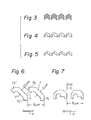
- Figures 3, 4, and 5 illustrate various tracks defined by well-known chevron, half-disk, and asymmetric chevron patterns, respectively.
- the half-disk and asymmetric chevron patterns are gap-tolerant patterns.
- Figure 6 illustrates an 8 ⁇ m period, 2 / um gap wide-gap track defined by one of several kinds of wide--gap patterns reported by A.H. Bobeck et al.
- the wide--gap pattern, designated by reference numeral 7 (7') is a hook-shaped or clubfoot-shaped pattern and has a first end portion (a leg) 7a (7a') and a second end portion (an arm) 7b (7b').
- the wide-gap track is defined by the hook-shaped patterns 7 (7') which are arranged in the bubble propagation direction P in such a manner that the arm 7b of the preceding pattern 7 is not parallel to the leg 7a' of the succeeding pattern 7' and is positioned back from the leg 7a' with respect to the propagation direction P and opposite the outer edge of the succeeding pattern 7', with a gap G therebetween.
- Figure 7 illustrates an 8 / um period, 2 / um gap track defined by conventional half-disk patterns.
- the adjacent end portions of the half-disk patterns are parallel to each other and are on the same level at the ends thereof with respect to the propagation direction P.
- Figure 9 illustrates the magnetic potential well depths of the 8 ⁇ m period, 2 / um gap wide-gap track illustrated in Fig. 6, which depths are measured by observing the real bubble motion in a quasi-static operation.
- the curve CF shows bubble collapse fields at each phase of a 58 Oe rotating drive field.
- the collapse field at point B of the pattern gradually decreases as the drive field is rotated to 337.5° while the collapse field at point C of the next pattern has already become higher than the free-bubble collapse field (FBC) at 315° and gradually increases with further drive field rotation.
- FBC free-bubble collapse field
- Figs. 10 and 11 illustrate the potential gradient across the pattern gap for the wide-gap track and the half-disk track, respectively.
- Figs. 10 and 11 illustrate the potential gradient across the pattern gap for the wide-gap track and the half-disk track, respectively.
- a designing point for a 4 ⁇ m period wide-gap track is to make the potential gradient between the elements as steep and smooth as possible by utilizing attractive, neutral, and repulsive magnetic poles.
- Figure 12 illustrates a 4 ⁇ m period wide-gap track scaled from the known 8 / um period wide-gap track shown in Fig. 6.
- Figures 13 and 14 illustrate 4 / um period wide-gap tracks defined by modified wide-gap patterns designed by the inventors of the present invention.
- the leg 8a is longer and the arm 8b is slightly longer than the leg and arm of the pattern 7A illustrated in Fig. 12.
- the leg 9 illustrated in Fig. 14 the leg 9a is wider and the arm 9b is slightly longer than the leg and arm of the pattern 8 illustrated in Fig. 13.
- the propagation characteristics of the tracks illustrated in Figs. 13 and 14 are illustrated in Fig. 15 by the curves L 3 and L 4 , respectively, under the conditions of a bubble diameter of 1.3 / um and a drive frequency of 100 kHz. These characteristics are superior to those of the track illustrated in Fig. 12.
- Figure 16 illustrates a 90° turn of a 8 ⁇ m period wide-gap permalloy track reported by A.H. Bobeck et al.
- reference numerals 10 and 11 designate first and second straight tracks for bubble propagation in the directions X and Y, respectively.
- the tracks 10 and 11 are the same as those illustrated in Fig. 6.
- a turn 12 which interconnects the first and second tracks 10 and 11 includes a hook-shaped permalloy pattern 15, which has the same configuration as the propagation patterns of the tracks 10 and 11.
- the pattern 15 has an end portion (an arm) 15a positioned adjacent to the end portions (arm and leg) of the end patterns 13 and 14 of the respective tracks 10 and 11.
- a steep and smooth magnetic potential gradient between the patterns 13 and 15 and between the patterns 15 and 14 cannot be obtained, and, accordingly, the propagation characteristics are poor, as is illustrated in Fig. 18 by the curve L 5 .
- Figure 17 illustrates an embodiment of the 90° turn of the 8 pm period wide-gap permalloy propagation track according to the present invention.
- reference numerals 20 and 21 designate first and second tracks which are substantially the same as the tracks 10 and 11, respectively, illustrated in Fig. 16.
- a turn 22 interconnecting the tracks 20 and 21 includes a crooked bar-shaped permalloy pattern 25 disposed between the end pattern 23 of the first track 20 and the end pattern 24 of the second track 21.
- the arm 23a of the end pattern 23 is positioned opposite the inner edge 25a of the pattern 25, with a gap G therebetween.
- the end portion 25b of the pattern 25 is positioned adjacent to the leg 24a of the end pattern 24, with a gap therebetween.
- the arm 23a of the pattern 23 is desirably substantially perpendicular to the inner edge 25a of the pattern 25.
- Bubble propagation in the track illustrated in Fig. 17 is now described.
- a bubble moves along the first track 20 in the direction X to the end pattern 23 and is trapped in the position "1" at phase ti of the drive field H R .
- the successive rotation of the drive field H causes the bubble to move successively into the position "2" of the arm 23a of the pattern 23 between phases t l and t 3 , into the position "3" of the end portion 25b of the pattern 25 between phases t 2 and t 3 , and into the position "4" of the leg 24a of the end pattern 24 of the second track 21 between phases t 3 and t 4 .
- Further successive rotation of the drive field H R causes the bubble to move, via the position "5", along the second track 21 in the direction Y.
- Figure 19 illustrates another embodiment of the 90° turn of the 8 ⁇ m period wide-gap track according to the present invention.
- This embodiment is basically the same as that illustrated in Fig. 17 except that the pattern 25A in the turn 22A has a different configuration than does the pattern 25 in the turn 22 of Fig. 17.
- the propagation characteristics of this embodiment are equal to or superior to those of the embodiment illustrated in Fig. 17.
- Figure 20 illustrates an embodiment of the 180° turn of the 8 pm period wide-gap permalloy track according to the present invention.
- reference numerals 30 and 31 designate first and second tracks which are the same as the tracks 20 and 21, respectively, illustrated in Fig. 17 except that bubble propagation is in the directions X and X'.
- a turn 32 interconnecting the tracks 30 and 31 includes a first, or main, crooked bar-shaped permalloy pattern 35 and a second, or auxiliary, crooked bar-shaped permalloy patter 36.
- the arm 33a of the end pattern 33 of the first track 30 is positioned opposite the inner edge 35a of the main crooked bar pattern 35, with a gap therebetween.
- the end portion 35b of the main pattern 35 is adjacent to the leg 34a of the end pattern 34 of the second track 31.
- the auxiliary pattern 36 is disposed in a region adjacent to the outer edge of the main pattern 35 so as to extend substantially parallel to the latter and has one end portion adjacent to the end portion 35b of the main pattern 35 and to the end pattern 34 of the second track 31.
- a bubble propagates along the first track 30 in the direction X and, from the pattern 33, via the pattern 35, to the pattern 34, and further along the second track 31 in the direction X'.
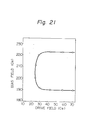
- a steep and smooth magnetic potential gradient between the patterns 33 and 35 and the patterns 35 and 34 is realized, and, accordingly, superior propagation characteristics as illustrated in Fig. 21 can be obtained.
- the auxiliary pattern 36 contributes to realization of the steep and smooth magnetic potential gradient between the patterns 35 and 34.
- Figures 22 and 23 illustrate further embodiments of the 180° turn of the 8 / um period wide-gap permalloy propagation track according to the present invention. These embodiments are basically the same as the embodiment illustrated in Fig. 20 except for the configurations of the main patterns 35A and 35B and the auxiliary patterns 36A and 36B of the turns 32A and 32B. The propagation characteristics of these tracks are equal to or superior to those of the embodiment illustrated in Fig. 20.
- Figures 24 and 25 illustrate embodiments of the 180° turn of the 4 ⁇ m period wide-gap permalloy track according to the present invention.
- reference numerals 40 and 41 designate first and second straight tracks for bubble propagation in the directions X and X', respectively, which tracks are defined by propagation patterns similar to the modified and improved wide-gap pattern illustrated in Fig. 13.
- a turn 42 includes a main crooked bar-shaped pattern 45 and an anuxiliary crooked bar-shaped pattern 46.
- the relationship in arrangement between the end patterns 43 and 44 of the tracks 40 and 41 and the patterns 45 and 46 of the turn 42 is the same as that in the embodiment illustrated in Fig. 20 except for the width of the gaps.
- the embodiment illustrated in Fig. 25 is basically the same as the embodiment illustrated in Fig. 24 except ; for the configuration of the patterns in the tracks 40A and 41A and the turn 42A.
- the auxiliary pattern 46A of the turn 42A has an end portion 47 which is remarkably different in configuration from the end portion of the auxiliary pattern 46 illustrated in Fig. 24.
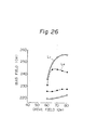
- the propagation characteristics of the tracks illustrated in Figs. 24 and 25 are the same as those illustrated in Figs. 26 and 27, respectively, provided that 5 Oe in-plane holding fields H 1 and H 2 are 5 selectively applied to the tracks as illustrated in Figs. 24 and 25.
- the curves L 7 and L 9 correspond to cases in which the field H 1 is applied, and the curves L 8 and L 10 correspond to cases in which the field H 2 is applied.
- the present invention makes it possible to realize a 4 ⁇ m period permalloy bubble propagation 'track in which, particularly, in the turn superior propagation character- istics are obtained, and, accordingly, a 4 ⁇ m period, 4 M b bubble memory can be obtained.
Landscapes
- Thin Magnetic Films (AREA)
Applications Claiming Priority (2)
| Application Number | Priority Date | Filing Date | Title |
|---|---|---|---|
| JP123767/82 | 1982-07-17 | ||
| JP57123767A JPS5916189A (ja) | 1982-07-17 | 1982-07-17 | 磁気バブルメモリ素子 |
Publications (3)
| Publication Number | Publication Date |
|---|---|
| EP0101187A2 true EP0101187A2 (fr) | 1984-02-22 |
| EP0101187A3 EP0101187A3 (en) | 1986-03-19 |
| EP0101187B1 EP0101187B1 (fr) | 1989-01-11 |
Family
ID=14868773
Family Applications (1)
| Application Number | Title | Priority Date | Filing Date |
|---|---|---|---|
| EP83304098A Expired EP0101187B1 (fr) | 1982-07-17 | 1983-07-14 | Dispositif de mémoire à bulles magnétique |
Country Status (5)
| Country | Link |
|---|---|
| US (1) | US4625297A (fr) |
| EP (1) | EP0101187B1 (fr) |
| JP (1) | JPS5916189A (fr) |
| CA (1) | CA1207444A (fr) |
| DE (1) | DE3378940D1 (fr) |
Cited By (1)
| Publication number | Priority date | Publication date | Assignee | Title |
|---|---|---|---|---|
| EP0155212A3 (fr) * | 1984-03-03 | 1989-03-15 | Fujitsu Limited | Dispositif de mémoire à bulles magnétiques |
Families Citing this family (2)
| Publication number | Priority date | Publication date | Assignee | Title |
|---|---|---|---|---|
| US6798691B1 (en) * | 2002-03-07 | 2004-09-28 | Silicon Magnetic Systems | Asymmetric dot shape for increasing select-unselect margin in MRAM devices |
| JP5299845B2 (ja) | 2009-03-27 | 2013-09-25 | 住友電装株式会社 | 自動車用ケーブル支持具 |
Family Cites Families (6)
| Publication number | Priority date | Publication date | Assignee | Title |
|---|---|---|---|---|
| US4261045A (en) * | 1979-06-29 | 1981-04-07 | International Business Machines Corporation | Magnetic bubble Y-bar corner |
| US4333163A (en) * | 1980-04-25 | 1982-06-01 | National Semiconductor Corporation | Bubble memory with increased gap tolerance between propagation elements |
| US4357682A (en) * | 1980-11-24 | 1982-11-02 | Bell Telephone Laboratories, Incorporated | Conductorless transfer for magnetic bubble memories |
| JPS57501803A (fr) * | 1980-11-24 | 1982-10-07 | ||
| US4355373A (en) * | 1980-11-24 | 1982-10-19 | Bell Telephone Laboratories, Incorporated | Magnetic bubble memory |
| JPS5916192A (ja) * | 1982-07-19 | 1984-01-27 | Fujitsu Ltd | 磁気バブル素子 |
-
1982
- 1982-07-17 JP JP57123767A patent/JPS5916189A/ja active Granted
-
1983
- 1983-07-13 CA CA000432330A patent/CA1207444A/fr not_active Expired
- 1983-07-14 US US06/513,657 patent/US4625297A/en not_active Expired - Fee Related
- 1983-07-14 DE DE8383304098T patent/DE3378940D1/de not_active Expired
- 1983-07-14 EP EP83304098A patent/EP0101187B1/fr not_active Expired
Cited By (1)
| Publication number | Priority date | Publication date | Assignee | Title |
|---|---|---|---|---|
| EP0155212A3 (fr) * | 1984-03-03 | 1989-03-15 | Fujitsu Limited | Dispositif de mémoire à bulles magnétiques |
Also Published As
| Publication number | Publication date |
|---|---|
| DE3378940D1 (en) | 1989-02-16 |
| CA1207444A (fr) | 1986-07-08 |
| JPS613026B2 (fr) | 1986-01-29 |
| US4625297A (en) | 1986-11-25 |
| JPS5916189A (ja) | 1984-01-27 |
| EP0101187A3 (en) | 1986-03-19 |
| EP0101187B1 (fr) | 1989-01-11 |
Similar Documents
| Publication | Publication Date | Title |
|---|---|---|
| US3723716A (en) | Single wall domain arrangement including fine-grained, field access pattern | |
| EP0255044B1 (fr) | Dispositif de mémoire à ligne Bloch | |
| US4247912A (en) | Magnetic bubble domain chip with enhanced propagation margins | |
| EP0101187A2 (fr) | Dispositif de mémoire à bulles magnétique | |
| EP0099750B1 (fr) | Dispositif de mémoire à bulles magnétiques | |
| US4079461A (en) | Gap tolerant bubble domain propagation circuits | |
| EP0044708B1 (fr) | Dispositif de mémoire à bulles magnétiques | |
| US3996572A (en) | Very high density gapless propagation structure for bubble domains | |
| CA1060990A (fr) | Mode de propagation de bulles magnetiques | |
| US3988722A (en) | Single sided, high density bubble domain propagation device | |
| US4164026A (en) | Contiguous element field access bubble lattice file | |
| US4283775A (en) | Contiguous disk bubble storage | |
| CA1165874A (fr) | Memoire a bulles magnetiques | |
| US4027297A (en) | Gapless magnetic bubble propagation path structure | |
| US4012726A (en) | Magnetic bubble replicator | |
| US4434476A (en) | Magnetic bubble memory device and method for operating the same | |
| Yamagishi et al. | Design and characteristics for a 4 µm period permalloy bubble device | |
| US4494216A (en) | Magnetic bubble memory device | |
| US4881198A (en) | Duplicator in a magnetic bubble memory and process for duplicating bubbles therein | |
| US4476544A (en) | Current-controlled magnetic domain memory | |
| US4357682A (en) | Conductorless transfer for magnetic bubble memories | |
| US4698786A (en) | Magnetic bubble memory device | |
| US4128896A (en) | One-level switch for magnetic bubble domain devices | |
| US3947830A (en) | Complementary transition structures for magnetic domain propagation | |
| EP0097524B1 (fr) | Dispositif de mémoire à bulles magnétiques |
Legal Events
| Date | Code | Title | Description |
|---|---|---|---|
| PUAI | Public reference made under article 153(3) epc to a published international application that has entered the european phase |
Free format text: ORIGINAL CODE: 0009012 |
|
| AK | Designated contracting states |
Designated state(s): DE FR GB NL |
|
| PUAL | Search report despatched |
Free format text: ORIGINAL CODE: 0009013 |
|
| AK | Designated contracting states |
Kind code of ref document: A3 Designated state(s): DE FR GB NL |
|
| 17P | Request for examination filed |
Effective date: 19860819 |
|
| 17Q | First examination report despatched |
Effective date: 19870818 |
|
| GRAA | (expected) grant |
Free format text: ORIGINAL CODE: 0009210 |
|
| AK | Designated contracting states |
Kind code of ref document: B1 Designated state(s): DE FR GB NL |
|
| REF | Corresponds to: |
Ref document number: 3378940 Country of ref document: DE Date of ref document: 19890216 |
|
| ET | Fr: translation filed | ||
| PLBE | No opposition filed within time limit |
Free format text: ORIGINAL CODE: 0009261 |
|
| STAA | Information on the status of an ep patent application or granted ep patent |
Free format text: STATUS: NO OPPOSITION FILED WITHIN TIME LIMIT |
|
| 26N | No opposition filed | ||
| PGFP | Annual fee paid to national office [announced via postgrant information from national office to epo] |
Ref country code: GB Payment date: 19920630 Year of fee payment: 10 |
|
| PGFP | Annual fee paid to national office [announced via postgrant information from national office to epo] |
Ref country code: FR Payment date: 19920730 Year of fee payment: 10 |
|
| PGFP | Annual fee paid to national office [announced via postgrant information from national office to epo] |
Ref country code: NL Payment date: 19920731 Year of fee payment: 10 |
|
| PGFP | Annual fee paid to national office [announced via postgrant information from national office to epo] |
Ref country code: DE Payment date: 19920922 Year of fee payment: 10 |
|
| PG25 | Lapsed in a contracting state [announced via postgrant information from national office to epo] |
Ref country code: GB Effective date: 19930714 |
|
| PG25 | Lapsed in a contracting state [announced via postgrant information from national office to epo] |
Ref country code: NL Effective date: 19940201 |
|
| GBPC | Gb: european patent ceased through non-payment of renewal fee |
Effective date: 19930714 |
|
| NLV4 | Nl: lapsed or anulled due to non-payment of the annual fee | ||
| PG25 | Lapsed in a contracting state [announced via postgrant information from national office to epo] |
Ref country code: FR Effective date: 19940331 |
|
| PG25 | Lapsed in a contracting state [announced via postgrant information from national office to epo] |
Ref country code: DE Effective date: 19940401 |
|
| REG | Reference to a national code |
Ref country code: FR Ref legal event code: ST |