EP0102035A2 - Elektrodenmaterial für Halbleitervorrichtungen - Google Patents
Elektrodenmaterial für Halbleitervorrichtungen Download PDFInfo
- Publication number
- EP0102035A2 EP0102035A2 EP83108171A EP83108171A EP0102035A2 EP 0102035 A2 EP0102035 A2 EP 0102035A2 EP 83108171 A EP83108171 A EP 83108171A EP 83108171 A EP83108171 A EP 83108171A EP 0102035 A2 EP0102035 A2 EP 0102035A2
- Authority
- EP
- European Patent Office
- Prior art keywords
- electrode material
- powders
- electrode
- semi
- present
- Prior art date
- Legal status (The legal status is an assumption and is not a legal conclusion. Google has not performed a legal analysis and makes no representation as to the accuracy of the status listed.)
- Withdrawn
Links
Images
Classifications
-
- H—ELECTRICITY
- H10—SEMICONDUCTOR DEVICES; ELECTRIC SOLID-STATE DEVICES NOT OTHERWISE PROVIDED FOR
- H10F—INORGANIC SEMICONDUCTOR DEVICES SENSITIVE TO INFRARED RADIATION, LIGHT, ELECTROMAGNETIC RADIATION OF SHORTER WAVELENGTH OR CORPUSCULAR RADIATION
- H10F77/00—Constructional details of devices covered by this subclass
- H10F77/20—Electrodes
- H10F77/206—Electrodes for devices having potential barriers
-
- H—ELECTRICITY
- H10—SEMICONDUCTOR DEVICES; ELECTRIC SOLID-STATE DEVICES NOT OTHERWISE PROVIDED FOR
- H10F—INORGANIC SEMICONDUCTOR DEVICES SENSITIVE TO INFRARED RADIATION, LIGHT, ELECTROMAGNETIC RADIATION OF SHORTER WAVELENGTH OR CORPUSCULAR RADIATION
- H10F77/00—Constructional details of devices covered by this subclass
- H10F77/20—Electrodes
- H10F77/206—Electrodes for devices having potential barriers
- H10F77/211—Electrodes for devices having potential barriers for photovoltaic cells
-
- Y—GENERAL TAGGING OF NEW TECHNOLOGICAL DEVELOPMENTS; GENERAL TAGGING OF CROSS-SECTIONAL TECHNOLOGIES SPANNING OVER SEVERAL SECTIONS OF THE IPC; TECHNICAL SUBJECTS COVERED BY FORMER USPC CROSS-REFERENCE ART COLLECTIONS [XRACs] AND DIGESTS
- Y02—TECHNOLOGIES OR APPLICATIONS FOR MITIGATION OR ADAPTATION AGAINST CLIMATE CHANGE
- Y02E—REDUCTION OF GREENHOUSE GAS [GHG] EMISSIONS, RELATED TO ENERGY GENERATION, TRANSMISSION OR DISTRIBUTION
- Y02E10/00—Energy generation through renewable energy sources
- Y02E10/50—Photovoltaic [PV] energy
Definitions
- This invention relates to an electrode material for semi-conductor devices, and particularly to an electrode material suitable for the production of semi-conductor elements having an electrode in a relatively rough pattern, such as solar cells, etc.
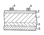
- Typical structure of a solar cell as a semi-conductor element is shown in the accompanying drawing, where light recipient side electrodes 4 and a back side electrode 5 are formed on the light recipient side and the back side, respectively, of a Si substrate 1 having an n layer 2 and a p layer in an n + /p/p + junction, and generally antireflective layers, etc. can be further provided on it.
- electroconductive paste a pasty mixture of metal powders, glass powders, etc. kneaded with an organic binder and an organic solvent (which will be hereinafter referred to as "electroconductive paste") is applied to a substrate by screen printing, etc., and fired, where generally silver powders are used as the metal powders.
- electroconductive paste Many kinds of such electroconductive paste are commercially available for forming electrodes of solar cell or for forming a thick film circuit.
- requirements for forming electrode of solar cell are high bonding strength of electrode, low contact resistance with silicon, no break-through of diffusion layer (small leak current), etc.
- An object of the present invention is to provide a very useful electrode material for semi-conductor devices such as solar cells, etc.
- an electrode material comprises silver (Ag) powders, at least one of zirconium (Zr), hafnium (Hf), vanadium ( V ), niobium (Nb), and tantalum (Ta), an organic binder and an organic solvent, and can further contain glass powder or palladium (Pd) powders.
- the present electrode material differs from the conventional electroconductive paste in that the present electrode material contains at least one metal of Zr, Hf, V, Nb and Ta.
- the present inventors have found that an electrode with a very low contact resistance to a substrate such as silicon, etc. can be formed from the present electrode material containing at least one of the said metals by printing and firing even at a relatively low temperature having no risk of junction breakage ( ⁇ 750°C).
- a thin insulating silicon oxide layer will be formed on the silicon surface by the oxygen contained in the firing atmosphere.
- an electroconductive paste containing a low melting glass based on lead oxide such a silicon oxide layer can be also formed by reaction of lead oxide with silicon. It seems that a silicon oxide layer formed on the silicon surface will much increase the contact resistance between the fired electrode and silicon substrate.
- the present electrode material it seems that a silicon oxide layer will be also formed in the same manner as above, but the metal contained in the present electrode material, that is, Zr, Hf, V, Nb, and/or Ta reacts with the silicon oxide layer, resulting in reduction of silicon oxide or formation of silicide compounds of these metals, and consequently it seems that the contact resistance between the electrode and the silicon substrate will be much lowered.
- Ag powders having particle sizes of less than 1 ⁇ m, cellulose-based compounds and polymethacrylate- based compounds as the organic binder, and polyhydric alcohol as the organic solvent can be particularly preferably used.
- metals of Zr, Hf, V, Nb and Ta in a powdery state, but powders of these metals have a high activity, and thus it is preferable to use the stabilized powders, that is, powders having a thin oxide layer on the powder surface.
- Zr, Hf, V, Nb, and Ta can be used alone or in a mixture of two or more of them. It is also possible to use alloy powders of two or more of them, or Ag powder with a coating of one or more of these metals.
- the present electrode material can contain glass, but glass can improve the bonding strength of formed electrode to the semi-conductor element, when contained, and can also improve the resistance of electrode to soldering.
- the present electrode material it is rather preferable for the present electrode material to contain glass particularly when solar cell electrodes are formed.
- the species of glass for use in the present invention are not particularly limited.
- the present electrode material can contain Pd powder, whereby the resistance of the formed electrode to soldering can be further improved. Furthermore, the present electrode material can contain Pt powders, whereby the bonding strength of the formed electrode can be improved.
- the present electrode material is used particularly for forming solar cell electrodes, it is preferable to use 0.5 - 30 parts by weight of at least one metal of Zr, Hf, V, Nb and Ta per 100 parts by weight of Ag powders. Below 0.5 parts by weight, the contact resistance of formed electrode to silicon substrate is increased, whereas above 30 parts by weight, the resistance of formed electrode is rather increased, resulting in possible reduction in the solar cell efficiency.
- Single Figure is a cross-sectional view showing a typical structure of solar cell, wherein 1 is a silicon substrate, 2 is an n layer, 3 is a p layer, 4 is a light recipient side electrode, and 5 is a back side electrode.
- a p-type silicon substrate (round wafer, 3 inches in diameter, specific resistance 1 - 5 ⁇ cm) with an n + layer, 0.3 - 0.5 ⁇ m deep, formed by ion implantation (specific resistance 1.5 x 10 -3 ⁇ cm) on one side and a p layer, 1 - 2 ⁇ m deep, by Al diffusion on the other side, was used.
- Said pasty electrode material was applied by screen printing onto the n + layer of the junction-formed silicon substrate in a comb pattern and onto the p + layer overall, and dried at 150°C for 10 minutes.
- the thus prepared solar cell was investigated for the current-voltage characteristics (I - V characteristics) that is, contact resistance of electrode, leak current at the reverse bias voltage (IV), fill factor (F.F.), open circuit voltage (Voc) and short circuit current (Isc). The results are shown in Table 1.
- the present electrode material has a sufficiently low contact resistance, when fired even at a relatively low temperature of 600°C, and also has no increase in leak current in spite of the n layer being as shallow as 0.3 - 0.5 ⁇ m, and is very ditinguished as compared with the conventional electroconductive paste.
- the present electrode materials containing Hf, V, Nb and Ta as the metals are shown.
- Metal powders of Hf, V, Nb and Ta with a thin oxide layer on the powder surface Ag powders having particle sizes of less than l ⁇ m and glass frits (based on lead borosilicate, zinc borosilicate and phosphate) were weighed out in various combinations as shown in Table 2, and thoroughly kneaded while adding thereto a viscous solution of 40 parts by weight of poly- isobutyl methacrylate and 0.5 parts by weight of a dispersant in 60 parts by weight of ⁇ -terpineol to prepare various pasty electrode materials having a viscosity of about 200 poises (share rate 100 sec -1 ).
- the thus prepared electrode materials were applied to the surfaces of the same junction-formed silicon substrates by screen printing, dried at 150°C for 10 minutes, and fired at 600°C for 10 minutes in a nitrogen gas atmosphere containing 5 ppm of oxygen.
- the thus prepared solar cells were investigated for their characteristics in the same manner as in Example 1, and the results are shown in Table 2 together with the components of the electrode materials.
- the present electrode materials containing Hf, V, Nb and Ta have a low contact resistance, and larger F.F. and Isc, and consequently considerably improved efficiency, as compared with Comparative Example 2 using no such metal powders.
- the leak current is all on the order of 10 6 A/cm 2 and there are no problems at all.
- Example 2 has very distinguished effects than the conventional electroconductive paste.
- the present electrode material is an epock-making material capable of forming an electrode with a low contact resistance without any junction breakage or increase in leak current to semi-conductor elements with shallow junction even at a relatively low firing temperature.
- a very highly efficient solar cell can be prepared by using the present electrode material in forming electrodes of solar cells, as compared with the conventional electroconductive paste.
- the present electrode material can be applied to a substrate by printing, and thus electrodes can be formed at a low cost with a high productivity. Thus, the present electrode material is industrially very useful. Furthermore the present electrode material can be also used in forming light-recipient elements other than the solar cell and also forming electrodes for other semi-conductor devices.
Landscapes
- Photovoltaic Devices (AREA)
- Conductive Materials (AREA)
- Electrodes Of Semiconductors (AREA)
Applications Claiming Priority (2)
| Application Number | Priority Date | Filing Date | Title |
|---|---|---|---|
| JP57143202A JPS5933868A (ja) | 1982-08-20 | 1982-08-20 | 半導体装置用電極材料 |
| JP143202/82 | 1982-08-20 |
Publications (2)
| Publication Number | Publication Date |
|---|---|
| EP0102035A2 true EP0102035A2 (de) | 1984-03-07 |
| EP0102035A3 EP0102035A3 (de) | 1986-03-26 |
Family
ID=15333246
Family Applications (1)
| Application Number | Title | Priority Date | Filing Date |
|---|---|---|---|
| EP83108171A Withdrawn EP0102035A3 (de) | 1982-08-20 | 1983-08-18 | Elektrodenmaterial für Halbleitervorrichtungen |
Country Status (3)
| Country | Link |
|---|---|
| US (1) | US4486232A (de) |
| EP (1) | EP0102035A3 (de) |
| JP (1) | JPS5933868A (de) |
Families Citing this family (16)
| Publication number | Priority date | Publication date | Assignee | Title |
|---|---|---|---|---|
| US5428249A (en) | 1992-07-15 | 1995-06-27 | Canon Kabushiki Kaisha | Photovoltaic device with improved collector electrode |
| JPH08148709A (ja) * | 1994-11-15 | 1996-06-07 | Mitsubishi Electric Corp | 薄型太陽電池の製造方法及び薄型太陽電池の製造装置 |
| US6071437A (en) * | 1998-02-26 | 2000-06-06 | Murata Manufacturing Co., Ltd. | Electrically conductive composition for a solar cell |
| US20060102228A1 (en) * | 2004-11-12 | 2006-05-18 | Ferro Corporation | Method of making solar cell contacts |
| US8093491B2 (en) | 2005-06-03 | 2012-01-10 | Ferro Corporation | Lead free solar cell contacts |
| US20080230119A1 (en) * | 2007-03-22 | 2008-09-25 | Hideki Akimoto | Paste for back contact-type solar cell |
| KR101623597B1 (ko) * | 2007-04-25 | 2016-05-23 | 헤레우스 프레셔스 메탈즈 노스 아메리카 콘쇼호켄 엘엘씨 | 은과 니켈 또는 은과 니켈 합금을 포함하는 후막 컨덕터 조성물 및 이로부터 제조된 태양 전지 |
| US8236598B2 (en) * | 2007-08-31 | 2012-08-07 | Ferro Corporation | Layered contact structure for solar cells |
| US20090211626A1 (en) * | 2008-02-26 | 2009-08-27 | Hideki Akimoto | Conductive paste and grid electrode for silicon solar cells |
| US20100037941A1 (en) * | 2008-08-13 | 2010-02-18 | E. I. Du Pont De Nemours And Company | Compositions and processes for forming photovoltaic devices |
| US8294024B2 (en) * | 2008-08-13 | 2012-10-23 | E I Du Pont De Nemours And Company | Processes for forming photovoltaic devices |
| US8840701B2 (en) * | 2008-08-13 | 2014-09-23 | E I Du Pont De Nemours And Company | Multi-element metal powders for silicon solar cells |
| US7976734B2 (en) * | 2008-09-10 | 2011-07-12 | E.I. Du Pont De Nemours And Company | Solar cell electrodes |
| US8710355B2 (en) | 2008-12-22 | 2014-04-29 | E I Du Pont De Nemours And Company | Compositions and processes for forming photovoltaic devices |
| EP2417607A1 (de) * | 2009-04-08 | 2012-02-15 | E. I. du Pont de Nemours and Company | Solarzellenelektrode |
| US10784383B2 (en) | 2015-08-07 | 2020-09-22 | E I Du Pont De Nemours And Company | Conductive paste composition and semiconductor devices made therewith |
Family Cites Families (10)
| Publication number | Priority date | Publication date | Assignee | Title |
|---|---|---|---|---|
| US3450545A (en) * | 1966-05-31 | 1969-06-17 | Du Pont | Noble metal metalizing compositions |
| DE2240493C3 (de) * | 1972-08-17 | 1978-04-27 | Siemens Ag, 1000 Berlin Und 8000 Muenchen | Durchdringungsverbundmetall als Kontaktwerkstoff für Vakuumschalter und Verfahren zu seiner Herstellung |
| US3951872A (en) * | 1973-12-03 | 1976-04-20 | P. R. Mallory & Co., Inc. | Electrical contact material |
| GB1497741A (en) * | 1976-02-02 | 1978-01-12 | Ferranti Ltd | Formation of contacts for semiconductor devices |
| GB1558764A (en) * | 1976-11-15 | 1980-01-09 | Ferranti Ltd | Formation of contacts for semiconductor devices |
| AU509758B2 (en) * | 1977-07-29 | 1980-05-22 | Matsushita Electric Industrial Co., Ltd. | Ohmic electrode to semiconductor device |
| US4219448A (en) * | 1978-06-08 | 1980-08-26 | Bernd Ross | Screenable contact structure and method for semiconductor devices |
| US4293451A (en) * | 1978-06-08 | 1981-10-06 | Bernd Ross | Screenable contact structure and method for semiconductor devices |
| US4256513A (en) * | 1978-10-19 | 1981-03-17 | Matsushita Electric Industrial Co., Ltd. | Photoelectric conversion device |
| US4366336A (en) * | 1980-10-16 | 1982-12-28 | Chevron Research Company | Age and heat stabilized photovoltaic cells |
-
1982
- 1982-08-20 JP JP57143202A patent/JPS5933868A/ja active Granted
-
1983
- 1983-08-17 US US06/523,857 patent/US4486232A/en not_active Expired - Fee Related
- 1983-08-18 EP EP83108171A patent/EP0102035A3/de not_active Withdrawn
Also Published As
| Publication number | Publication date |
|---|---|
| EP0102035A3 (de) | 1986-03-26 |
| JPS5933868A (ja) | 1984-02-23 |
| JPH023554B2 (de) | 1990-01-24 |
| US4486232A (en) | 1984-12-04 |
Similar Documents
| Publication | Publication Date | Title |
|---|---|---|
| US4486232A (en) | Electrode material for semi-conductor devices | |
| US4219448A (en) | Screenable contact structure and method for semiconductor devices | |
| US4235644A (en) | Thick film silver metallizations for silicon solar cells | |
| US4293451A (en) | Screenable contact structure and method for semiconductor devices | |
| KR101552369B1 (ko) | 금속유기 변성제를 갖는 전도성 잉크 | |
| EP2306468B1 (de) | Leitfähige Zusammensetzungen und Verfahren zu ihrer Verwendung bei der Herstellung von Halbleitervorrichtungen | |
| US6071437A (en) | Electrically conductive composition for a solar cell | |
| US4737197A (en) | Solar cell with metal paste contact | |
| JP3255921B2 (ja) | 改良した太陽電池及びその製作方法 | |
| EP0059348B1 (de) | Elektrisch leitende Paste zum Einbrennen auf einem keramischen Körper für die Herstellung von Kondensatoren, Varistoren usw. | |
| EP1713093A2 (de) | Elektrisch leitfähige Dickschichtzusammensetzung, Elektrode und daraus hergestellte Solarzelle | |
| EP2698827A1 (de) | Elektrodenpastenzusammensetzung, solarzellen element und solarzelle | |
| EP2696353B1 (de) | Pastenzusammensetzung für elektroden und solarzelle damit | |
| JP3760361B2 (ja) | 太陽電池用導電性組成物 | |
| US4940849A (en) | Metallizing paste | |
| JPS6244864B2 (de) | ||
| EP2607327A1 (de) | Dickfilmzusammensetzung mit Antimonoxid und ihre Verwendung bei der Herstellung von Halbleiterbauelementen | |
| US5411601A (en) | Substrate for solar cell and solar cell employing the substrate | |
| JPH0773731A (ja) | 厚膜導電性ペースト組成物 | |
| JPH023555B2 (de) | ||
| JPH0337751B2 (de) | ||
| EP0054706B1 (de) | Verfahren zur Metallisierung einer Siliziumsolarzelle | |
| JPH023553B2 (de) | ||
| JPS59168668A (ja) | 半導体装置用電極材料 | |
| Dubey | Application of thick film techniques to the manufacture of solar cells |
Legal Events
| Date | Code | Title | Description |
|---|---|---|---|
| PUAI | Public reference made under article 153(3) epc to a published international application that has entered the european phase |
Free format text: ORIGINAL CODE: 0009012 |
|
| AK | Designated contracting states |
Designated state(s): DE FR |
|
| PUAL | Search report despatched |
Free format text: ORIGINAL CODE: 0009013 |
|
| AK | Designated contracting states |
Kind code of ref document: A3 Designated state(s): DE FR |
|
| 17P | Request for examination filed |
Effective date: 19860401 |
|
| 17Q | First examination report despatched |
Effective date: 19871009 |
|
| STAA | Information on the status of an ep patent application or granted ep patent |
Free format text: STATUS: THE APPLICATION HAS BEEN WITHDRAWN |
|
| 18W | Application withdrawn |
Withdrawal date: 19880812 |
|
| RIN1 | Information on inventor provided before grant (corrected) |
Inventor name: OKUNAKA, MASAAKI Inventor name: ISOGAI, TOKIO Inventor name: NAKATANI, MITSUO Inventor name: YOKONO, HITOSHI Inventor name: MATSUYAMA, HARUHIKO Inventor name: SAITOH, TADASHI Inventor name: MIDORIKAWA, SUMIYUKI |