EP0102262A1 - Kryostatvorrichtung mit geringen Abmessungen für Photodetektoren - Google Patents
Kryostatvorrichtung mit geringen Abmessungen für Photodetektoren Download PDFInfo
- Publication number
- EP0102262A1 EP0102262A1 EP19830401372 EP83401372A EP0102262A1 EP 0102262 A1 EP0102262 A1 EP 0102262A1 EP 19830401372 EP19830401372 EP 19830401372 EP 83401372 A EP83401372 A EP 83401372A EP 0102262 A1 EP0102262 A1 EP 0102262A1
- Authority
- EP
- European Patent Office
- Prior art keywords
- cryostatic device
- cryostatic
- finger
- base
- wall
- Prior art date
- Legal status (The legal status is an assumption and is not a legal conclusion. Google has not performed a legal analysis and makes no representation as to the accuracy of the status listed.)
- Granted
Links
Images


Classifications
-
- F—MECHANICAL ENGINEERING; LIGHTING; HEATING; WEAPONS; BLASTING
- F17—STORING OR DISTRIBUTING GASES OR LIQUIDS
- F17C—VESSELS FOR CONTAINING OR STORING COMPRESSED, LIQUEFIED OR SOLIDIFIED GASES; FIXED-CAPACITY GAS-HOLDERS; FILLING VESSELS WITH, OR DISCHARGING FROM VESSELS, COMPRESSED, LIQUEFIED, OR SOLIDIFIED GASES
- F17C3/00—Vessels not under pressure
- F17C3/02—Vessels not under pressure with provision for thermal insulation
- F17C3/08—Vessels not under pressure with provision for thermal insulation by vacuum spaces, e.g. Dewar flask
- F17C3/085—Cryostats
-
- G—PHYSICS
- G01—MEASURING; TESTING
- G01J—MEASUREMENT OF INTENSITY, VELOCITY, SPECTRAL CONTENT, POLARISATION, PHASE OR PULSE CHARACTERISTICS OF INFRARED, VISIBLE OR ULTRAVIOLET LIGHT; COLORIMETRY; RADIATION PYROMETRY
- G01J5/00—Radiation pyrometry, e.g. infrared or optical thermometry
- G01J5/02—Constructional details
- G01J5/06—Arrangements for eliminating effects of disturbing radiation; Arrangements for compensating changes in sensitivity
- G01J5/061—Arrangements for eliminating effects of disturbing radiation; Arrangements for compensating changes in sensitivity by controlling the temperature of the apparatus or parts thereof, e.g. using cooling means or thermostats
Definitions
- the present invention relates to a small cryostatic device for photodetectors.
- the detectors In order to have the greatest possible sensitivity to radiation, certain detectors such as infrared detectors must operate at a very low ambient temperature. To obtain this result, the detectors are generally mounted in cryostatic devices of the type comprising a finger worn at very low temperature on which are mounted the detector or detectors to be cooled and which is surrounded by a wall forming with said finger a sealed enclosure.
- the wall is provided on the part facing the detectors with a window made of a material transparent to the radiation to be detected.
- the enclosure is also placed under vacuum, in general using a pumping pipe, in order to avoid thermal losses around the cold finger.
- the cold finger is conventionally made of glass, the external wall being made of glass or metal. The use of glass causes certain problems.
- the cryostatic device due to its hot malleability, the cryostatic device easily deforms when sealing the two parts and it is difficult to obtain precise dimensions.
- the machining and the rectification of glass are delicate operations. It is therefore difficult to produce a cryostatic device at low cost, the external wall of which can serve as a positioning face. Consequently, it is necessary to use additional parts for the positioning of the cryostatic device:
- the cryostatic device is mounted in a precise mechanical part fitting onto the external wall of the cryostatic device proper. However, this mechanical part increases the mass and the bulk of the cryostatic device.
- the detectors are connected to the treatment by conductors of which the number is a function of the number of detectors mounted in the cryostatic device.
- the conductors must pass through the enclosure of the cryostatic device in leaktight manner. This can be done in many ways either at the level of the seal between the two parts constituting the finger and the external wall or by passing directly through the glass or the metal of the external wall. In the case of a passage at the level of the seal, it is necessary to use an additional insulating part, in general, of polyimide on which the conductors are engraved.
- the interval between two conductors must be sufficient, which limits the number of conductors at the output as a function of the external perimeter of the finger.
- infrared detectors in particular, are increasingly used in so-called "on-board” equipment. We therefore sought to minimize the size and weight of the cryostatic device.
- the present invention therefore has the aim of producing a cryostatic device for photodetectors which has reduced dimensions compared to the devices of the prior art.
- the present invention also aims to produce a cryostatic device for photodetectors which does not require the use of an additional positioning part.
- Another object of the present invention is to produce a cryostatic device for photodetectors having a long service life despite its small dimensions due to the obtaining of a relatively high and stable vacuum.
- the present invention likewise aims to produce a cryostatic device of small dimensions for photodetectors comprising a high number of conductors at the output which allows to cool a large number of photodetectors.
- the present invention therefore has as its object a cryostatic device in which the various elements constituting the cryostatic device itself are made of materials having stable mechanical properties allowing precise machining or molding of these elements.
- the small cryostatic device for photodetectors -in accordance with the present invention comprises a finger worn at very low temperature on the end of which is fixed at least one detector and a wall surrounding the cold finger to form with it a vacuum enclosure, a window in a material. transparent to the radiation to be detected being fixed on the wall opposite the detector and it is characterized in that the cold finger is made of a waterproof or sealed ceramic with low thermal conductivity, the cold finger being sealed so as to allow the passage of the conductors electrical to a base made of an insulating material with coefficient of thermal expansion compatible with that of the finger and having precise mechanical properties, base on which the external wall of the enclosure is mounted.
- the ceramics which can be used to make the cold finger mention may be made of forsterite, zirconia, mullite, soapstone.
- a porous ceramic such as a porous soapstone, it can be made waterproof by enameling.
- the base is also made of ceramic. In this case, it is very easy to make a tight mineral seal between the finger and the base.
- the external peripheral contour of the base is used as a positioning means. Therefore, this outline is preferably of polygonal or revolution shape and has a positioning index.
- the conductors are deposited directly on the finger cold by coating, spraying, soaking or evaporation under vacuum.
- the external surface of the cold finger can be grooved.
- the external wall of the cryostatic device is made of a ceramic, a metal or a metal alloy having a coefficient of thermal expansion corresponding substantially to that of the base.
- the metal alloy used is preferably an iron-nickel alloy such as Kovar (registered trademark) and Dilver P (registered trademark).
- the outer wall is tightly mounted on the base using a seal obtained by creep of an indium wire or toroid.
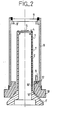
- the reference 1 designates the finger which must be worn at very low temperature.
- the finger 1 is made of a gas-tight ceramic with low thermal conductivity such as forsterite, zirconia, mullite, steatite.
- the finger 1 can also be made of a porous ceramic made waterproof, for example, by enameling.
- the finger 1 has a cylindrical main part which is bored to receive in its bore 2 a cryogenerator not shown.
- the cryogenerator can be constituted by any known cryogenerator such as a Joule Thomson expansion probe.
- the table 4 can receive a mosaic of detectors comprising 32x32 elements and has a useful diameter of 4 to 5 mm.
- the table brought to low temperature by the cryogenerator must quickly transmit heat. As a result, it is made of a material which is a good conductor of heat, the coefficient of thermal expansion of which is compatible with that of finger 1.
- the table is preferably made either of metal such as platinum, copper, molybdenum, etc., or of ceramic such as alumina, beryllium oxide, etc.
- the table 4 is sealed in a leaktight manner on the cylindrical part of the finger 1 either with an enamel or a suitable glass ceramic.
- the sheet of conductors 6 is deposited directly on the finger 1.
- This sheet of conductors 6 extends from the cold table 4 to the end of the conical part l 'namely the outside of the cryostatic device.
- This layer of conductors can be produced in different ways. By way of illustration, we will describe below various methods of producing said sheet.
- the sheet of conductors can be produced by depositing a conductive layer over the entire external surface of the finger.
- Said layer can be formed by a thin layer obtained, for example, by vacuum evaporation or by a thick layer produced by coating, spraying or dipping with a paste for screen printing.
- the conductors are then produced in this layer either by mechanical machining, or by laser machining, or by tracing with a hard point or by photolithography.
- the sheet of conductors can be obtained by evaporation under vacuum through a mask or by evaporation under vacuum through a slot.
- This last method makes it possible to vary the pitch of the conductors and, possibly, to form wider conductors by juxtaposing them.
- the slit is preferably kept fixed, the finger being moved in rotation under the slit after each evaporation using for example a stepping motor.
- the finger 1 is provided, at least in the part which must receive the conductors, with grooves 7 (one of these grooves has been shown in dashed lines by way of illustration in FIG. 2 ).
- the grooves 7 are produced either by molding or by machining.
- the width of the grooves corresponds to the width of the conductors and their pitch to the pitch of the conductors.
- a thick layer of screen-printing paste having a thickness of 9 to 10 ⁇ m is deposited on the cold finger, or a thin chromium-gold layer for example, obtained by evaporation under vacuum.
- the conductive layer deposited on the raised parts is then removed by machining using a grinding wheel or an abrasive cloth.
- the outputs of the detectors 5 are connected directly to the sheet of conductors 6 either by ultrasonic welding or by evaporation through a mask.
- the cryostatic device of the present invention comprises an external wall 8 which surrounds the finger 1 and on which is mounted, on the part facing the detectors 5, a window 9 made of a material transparent to the radiation to be detected.
- the wall 8 is constituted by a cylindrical envelope and comprises at one of its ends an internal annular stop 8 'intended to receive the window 9.
- the other end of the external wall 8 is mounted on a base 10 itself sealed on the finger 1, the assembly forming an enclosure capable of being placed under vacuum.
- the base 10 is constituted by a sleeve, the central bore of which has a part cylindrical 10 'extending by a conical part 10 "corresponding to the conical part l' of the finger so as to come to fit exactly on said part.
- the base 10 is made of an electrically insulating material , having stable and precise mechanical properties and a coefficient of thermal expansion equivalent to that of the finger. Consequently, the base is made of ceramic, preferably in the same ceramic as that of finger 1 and it is sealed on the part 1 'of the finger using an enamel or a ceramic glass, this type of sealing leaving intact the sheet of conductors 6 extending over part l. We therefore obtain a direct passage of the sheet of conductors 6 through the seal.
- the window 9 is preferably made of germanium.
- the window 9 can conventionally be glued against the stop 8 ′ of the wall 8. However, it will preferably be sealed on this stop using an indium wire as will be explained in detail below.
- the wall 8 which is also sealed on the base 10 must be made of a material whose coefficient of thermal expansion is compatible with that of the window and the base. Because although the sealing of these elements - is carried out cold as explained below, in most cases, the conditions of use are such that the equipment must operate in a very wide temperature range generally between - 40 ° C and + 70 ° C while keeping the seal watertight.
- the wall 8 is made either of ceramic or of a compatible metal such as platinum or of a metal alloy based on iron-nickel such as Kovar (registered trademark) and Dilver P (registered trademark). In some cases, the wall 8 will be made of a metal or magnetic alloy to provide electromagnetic shielding for protection of the detectors.
- the base being made of a material having precise mechanical properties which can be easily machined or molded, it can be easily used as a means of axial and rotational positioning of the cryostatic device.
- the external peripheral contour 10 "'of the base is cylindrical and includes an indexing means (not shown in the drawings) such as a notch or a slot.
- this part of the base could have a polygonal, elliptical or any other form of revolution.
- At least one getter 11 is implanted in holes 12 provided in the base 10.
- the getter is intended, when activated, to maintain the vacuum in the enclosure formed mainly by the finger 1, the base 10 and the outer wall 8.
- two. conductors are deposited on the base 10 to connect the legs of the getter to an external source allowing its activation by Joule effect.
- the getter is sealed in the hole 12 either by using an enamel or by using a screen-printing paste which, in addition to sealing, ensures the electrical contact between the conductors and the tabs.
- the sleeve constituting the base 10 has been machined or molded so that its external surface has two recesses 16, 17, the first having a width substantially equal to the thickness of the wall 8.
- An annular ring 18 is mounted against the recess 17 so as to form a groove, then the external wall mounted in a vacuum housing is inserted and pressed into the groove, after pumping and steaming of the 'together so as to creep the indium wire and transform it into a film 20 which fills the entire space between the ring 18, the recess 16 and the base 10.
- cryostatic device which can have very small dimensions while having a large number of outlets.
- the cryostatic device has a diameter of 12 mm and a length of less than 40 mm with 36 conductors at the outlet.
- the cryostatic device according to the invention also has the advantage of being simple, compact, precise with a reduced cost price.
- cryostatic device of the present invention can be provided with any known device improving its performance. It finds its use in particular in infrared self-directors and in infrared portable cameras but also in all equipment requiring cooled detectors of small dimensions.
Landscapes
- Physics & Mathematics (AREA)
- Engineering & Computer Science (AREA)
- Thermal Sciences (AREA)
- Mechanical Engineering (AREA)
- General Engineering & Computer Science (AREA)
- General Physics & Mathematics (AREA)
- Spectroscopy & Molecular Physics (AREA)
- Photometry And Measurement Of Optical Pulse Characteristics (AREA)
- Containers, Films, And Cooling For Superconductive Devices (AREA)
- Cooling Or The Like Of Electrical Apparatus (AREA)
Applications Claiming Priority (2)
| Application Number | Priority Date | Filing Date | Title |
|---|---|---|---|
| FR8212467A FR2530382B1 (fr) | 1982-07-16 | 1982-07-16 | Dispositif cryostatique de faibles dimensions pour photodetecteurs |
| FR8212467 | 1982-07-16 |
Publications (2)
| Publication Number | Publication Date |
|---|---|
| EP0102262A1 true EP0102262A1 (de) | 1984-03-07 |
| EP0102262B1 EP0102262B1 (de) | 1987-06-10 |
Family
ID=9276034
Family Applications (1)
| Application Number | Title | Priority Date | Filing Date |
|---|---|---|---|
| EP19830401372 Expired EP0102262B1 (de) | 1982-07-16 | 1983-07-04 | Kryostatvorrichtung mit geringen Abmessungen für Photodetektoren |
Country Status (5)
| Country | Link |
|---|---|
| US (1) | US4487037A (de) |
| EP (1) | EP0102262B1 (de) |
| JP (1) | JPS5927595A (de) |
| DE (1) | DE3372014D1 (de) |
| FR (1) | FR2530382B1 (de) |
Cited By (2)
| Publication number | Priority date | Publication date | Assignee | Title |
|---|---|---|---|---|
| FR2611404A1 (fr) * | 1987-02-27 | 1988-09-02 | Mitsubishi Electric Corp | Detecteur de rayons infrarouges |
| EP0350265A3 (de) * | 1988-07-05 | 1991-01-23 | General Electric Company | Wärmeleitende, elektrisch isolierende Verbindung |
Families Citing this family (17)
| Publication number | Priority date | Publication date | Assignee | Title |
|---|---|---|---|---|
| US4565925A (en) * | 1983-08-10 | 1986-01-21 | Ford Aerospace & Communications Corporation | Infrared detector dewar with all-Kovar leads, and method of making the same |
| US4597175A (en) * | 1983-08-10 | 1986-07-01 | Ford Aerospace & Communications Corporation | Method for making infrared detector dewar |
| DE3337194A1 (de) * | 1983-10-13 | 1985-04-25 | Telefunken electronic GmbH, 7100 Heilbronn | Gehaeuse fuer ein optoelektronisches halbleiterbauelement |
| FR2571128B1 (fr) * | 1984-10-02 | 1986-11-14 | Telecommunications Sa | Dispositif cryostatique pour photodetecteurs |
| US4645931A (en) * | 1985-03-15 | 1987-02-24 | Honeywell Inc. | Detector dewar assembly |
| US4833898A (en) * | 1987-01-07 | 1989-05-30 | Ford Aerospace & Communications Corporation | Multi-detector dewar |
| US4918929A (en) * | 1987-07-01 | 1990-04-24 | Ford Aerospace Corporation | Multi-detector dewar |
| JPH0335271Y2 (de) * | 1987-10-31 | 1991-07-25 | ||
| FR2629912B1 (fr) * | 1988-08-05 | 1992-01-10 | Detecteurs Infrarouges Ste Fse | Dispositif de detection infra-rouge fonctionnant a basse temperature |
| US4918312A (en) * | 1988-11-23 | 1990-04-17 | Santa Barbara Research Center | Dewar coldfinger |
| JP2763355B2 (ja) * | 1989-12-06 | 1998-06-11 | 富士通株式会社 | 赤外線検知装置 |
| US5017786A (en) * | 1989-12-19 | 1991-05-21 | Honeywell Inc. | V2 O3 protection for IR detector arrays against intense thermal radiation |
| JPH0536995A (ja) * | 1991-08-01 | 1993-02-12 | Fujitsu Ltd | 赤外線検知器及び該検知器に用いられる内筒への配線パターンの形成方法 |
| GB9617175D0 (en) * | 1996-08-15 | 1996-09-25 | Univ Aberdeen | Liquid gas cryostat |
| FR3008825B1 (fr) * | 2013-07-18 | 2016-12-09 | Soc Francaise De Detecteurs Infrarouges - Sofradir | Doigt froid ameliore et dispositif de detection comportant le doigt froid |
| RU183130U1 (ru) * | 2018-04-20 | 2018-09-12 | Акционерное общество "Московский завод "САПФИР" | Криостат для приемников излучения |
| CN114353953B (zh) * | 2022-01-13 | 2024-04-12 | 浙江珏芯微电子有限公司 | 一种用于快速制冷的杜瓦冷头及红外探测器杜瓦组件 |
Citations (4)
| Publication number | Priority date | Publication date | Assignee | Title |
|---|---|---|---|---|
| US3080542A (en) * | 1959-01-02 | 1963-03-05 | Santa Barbara Res Ct | Infrared detector and method of manufacture thereof |
| US3259865A (en) * | 1964-01-06 | 1966-07-05 | Micro State Electronics Corp | Dewar for cryogenic cooling of solid state device |
| US3851173A (en) * | 1973-06-25 | 1974-11-26 | Texas Instruments Inc | Thermal energy receiver |
| US4059764A (en) * | 1968-08-13 | 1977-11-22 | Texas Instruments Incorporated | Multi-element infra red sensors |
Family Cites Families (6)
| Publication number | Priority date | Publication date | Assignee | Title |
|---|---|---|---|---|
| US3358463A (en) * | 1966-07-15 | 1967-12-19 | Lockheed Aircraft Corp | Integrated superconducting magnetcryostat system |
| DE1751051C3 (de) * | 1968-03-26 | 1974-01-03 | Siemens Ag, 1000 Berlin U. 8000 Muenchen | Kryostat mit einer Vakuumkammer |
| US4206354A (en) * | 1976-07-09 | 1980-06-03 | Honeywell Inc. | Axial matrix Dewar |
| US4118947A (en) * | 1977-05-19 | 1978-10-10 | Selenia-Industrie Elettroniche Associate S.P.A. | Low thermal loss cryogenic containers for infrared radiation detecting devices, with integrated feed-through connections |
| US4325530A (en) * | 1978-03-02 | 1982-04-20 | The United States Of America As Represented By The United States Department Of Energy | Cryogenic structural support |
| US4340405A (en) * | 1980-10-29 | 1982-07-20 | The United States Of America As Represented By The United States Department Of Energy | Apparatus and method for maintaining low temperatures about an object at a remote location |
-
1982
- 1982-07-16 FR FR8212467A patent/FR2530382B1/fr not_active Expired
-
1983
- 1983-07-04 EP EP19830401372 patent/EP0102262B1/de not_active Expired
- 1983-07-04 DE DE8383401372T patent/DE3372014D1/de not_active Expired
- 1983-07-08 US US06/512,147 patent/US4487037A/en not_active Expired - Fee Related
- 1983-07-15 JP JP58129275A patent/JPS5927595A/ja active Pending
Patent Citations (4)
| Publication number | Priority date | Publication date | Assignee | Title |
|---|---|---|---|---|
| US3080542A (en) * | 1959-01-02 | 1963-03-05 | Santa Barbara Res Ct | Infrared detector and method of manufacture thereof |
| US3259865A (en) * | 1964-01-06 | 1966-07-05 | Micro State Electronics Corp | Dewar for cryogenic cooling of solid state device |
| US4059764A (en) * | 1968-08-13 | 1977-11-22 | Texas Instruments Incorporated | Multi-element infra red sensors |
| US3851173A (en) * | 1973-06-25 | 1974-11-26 | Texas Instruments Inc | Thermal energy receiver |
Non-Patent Citations (1)
| Title |
|---|
| W. FASTOWSKI et al.: "Kryotechnik", 1970, pages 312-321, chapitre 7.3 "Kryostaten", Akademie-Verlag, Berlin, DE. * |
Cited By (3)
| Publication number | Priority date | Publication date | Assignee | Title |
|---|---|---|---|---|
| FR2611404A1 (fr) * | 1987-02-27 | 1988-09-02 | Mitsubishi Electric Corp | Detecteur de rayons infrarouges |
| US4880979A (en) * | 1987-02-27 | 1989-11-14 | Mitisubishi Denki Kabushiki Kaisha | Infrared ray detector |
| EP0350265A3 (de) * | 1988-07-05 | 1991-01-23 | General Electric Company | Wärmeleitende, elektrisch isolierende Verbindung |
Also Published As
| Publication number | Publication date |
|---|---|
| FR2530382B1 (fr) | 1985-06-07 |
| DE3372014D1 (en) | 1987-07-16 |
| US4487037A (en) | 1984-12-11 |
| JPS5927595A (ja) | 1984-02-14 |
| EP0102262B1 (de) | 1987-06-10 |
| FR2530382A1 (fr) | 1984-01-20 |
Similar Documents
| Publication | Publication Date | Title |
|---|---|---|
| EP0102262B1 (de) | Kryostatvorrichtung mit geringen Abmessungen für Photodetektoren | |
| CH674263A5 (de) | ||
| FR2822543A1 (fr) | Detecteur de temperature | |
| EP0490764A1 (de) | Halbleiter-Durchflusssensor | |
| EP0544367B1 (de) | Kapazitiver Sensor mit leitender Frontseite, zur Bildung einer Kondensatorarmatur und einem mineralisierten abgeschirmten Koaxialkabel | |
| FR2703869A1 (fr) | Source de rayonnement thermique modulable électriquement et procédé pour sa fabrication. | |
| WO1992019943A1 (fr) | Procede et dispositif d'etalonnage d'un pyrometre optique et plaquettes etalons correspondantes | |
| EP0447295A1 (de) | Temperaturfühlerelement und Sonde mit einem solchen Element | |
| EP0231695A1 (de) | Fast-adiabatischer Kalorienmesser für das Messen der Energie, transportiert durch eine Strahlung | |
| FR2827707A1 (fr) | Procede de realisation d'un detecteur bolometrique et detecteur realise selon ce procede | |
| EP2715296A1 (de) | Spektroskopischer detektor und entsprechendes verfahren | |
| FR2570567A1 (fr) | Agencement d'hydrophone | |
| EP0044790A1 (de) | Sensor für die Gasanalyse | |
| EP0148703B1 (de) | Verfahren zur Temperaturkompensation eines photoleitenden Detektors | |
| US3080542A (en) | Infrared detector and method of manufacture thereof | |
| EP0231778B1 (de) | Abgeschlossener Gaslaser | |
| EP0117230B1 (de) | Fühler zum Messen der Sauerstoffkonzentration in Gasen | |
| EP0008275A1 (de) | Steckverbinder mit einer automatischen Regeleinrichtung zur Temperaturstabilisierung wenigstens eines Verbindungspunktes | |
| EP0323937B1 (de) | Trägerstruktur für Gassensoren | |
| FR2461252A1 (fr) | Detecteur d'oxygene a electrolyte solide et procede de fabrication du detecteur | |
| EP0026126A1 (de) | Verfahren zum Messen eines ständigen Neutronenflusses und Apparat zur Durchführung dieses Verfahrens | |
| FR2538099A1 (fr) | Amorce electrique a element resistif | |
| EP0117810A1 (de) | Anordnung zum Überwachen von beweglichen elektrischen Ladungen in einem in MOS Technologie ausgeführten integrierten Schaltkreis | |
| FR2595877A1 (fr) | Laser a haute performance, procede pour sa fabrication et gyroscope l'utilisant | |
| CA2395646C (fr) | Condensateur a haute stabilite thermique pour lignes electriques de type blindees |
Legal Events
| Date | Code | Title | Description |
|---|---|---|---|
| PUAI | Public reference made under article 153(3) epc to a published international application that has entered the european phase |
Free format text: ORIGINAL CODE: 0009012 |
|
| AK | Designated contracting states |
Designated state(s): DE GB IT SE |
|
| 17P | Request for examination filed |
Effective date: 19840322 |
|
| GRAA | (expected) grant |
Free format text: ORIGINAL CODE: 0009210 |
|
| AK | Designated contracting states |
Kind code of ref document: B1 Designated state(s): DE GB IT SE |
|
| ITF | It: translation for a ep patent filed | ||
| REF | Corresponds to: |
Ref document number: 3372014 Country of ref document: DE Date of ref document: 19870716 |
|
| PLBE | No opposition filed within time limit |
Free format text: ORIGINAL CODE: 0009261 |
|
| 26N | No opposition filed | ||
| ITTA | It: last paid annual fee | ||
| PGFP | Annual fee paid to national office [announced via postgrant information from national office to epo] |
Ref country code: SE Payment date: 19940620 Year of fee payment: 12 Ref country code: DE Payment date: 19940620 Year of fee payment: 12 |
|
| PGFP | Annual fee paid to national office [announced via postgrant information from national office to epo] |
Ref country code: GB Payment date: 19940621 Year of fee payment: 12 |
|
| EAL | Se: european patent in force in sweden |
Ref document number: 83401372.4 |
|
| PG25 | Lapsed in a contracting state [announced via postgrant information from national office to epo] |
Ref country code: GB Effective date: 19950704 |
|
| PG25 | Lapsed in a contracting state [announced via postgrant information from national office to epo] |
Ref country code: SE Effective date: 19950705 |
|
| GBPC | Gb: european patent ceased through non-payment of renewal fee |
Effective date: 19950704 |
|
| PG25 | Lapsed in a contracting state [announced via postgrant information from national office to epo] |
Ref country code: DE Effective date: 19960402 |
|
| EUG | Se: european patent has lapsed |
Ref document number: 83401372.4 |