EP0117810A1 - Anordnung zum Überwachen von beweglichen elektrischen Ladungen in einem in MOS Technologie ausgeführten integrierten Schaltkreis - Google Patents
Anordnung zum Überwachen von beweglichen elektrischen Ladungen in einem in MOS Technologie ausgeführten integrierten Schaltkreis Download PDFInfo
- Publication number
- EP0117810A1 EP0117810A1 EP84400338A EP84400338A EP0117810A1 EP 0117810 A1 EP0117810 A1 EP 0117810A1 EP 84400338 A EP84400338 A EP 84400338A EP 84400338 A EP84400338 A EP 84400338A EP 0117810 A1 EP0117810 A1 EP 0117810A1
- Authority
- EP
- European Patent Office
- Prior art keywords
- plate
- housing
- silicon
- integrated circuit
- conductive membrane
- Prior art date
- Legal status (The legal status is an assumption and is not a legal conclusion. Google has not performed a legal analysis and makes no representation as to the accuracy of the status listed.)
- Granted
Links
Images
Classifications
-
- G—PHYSICS
- G01—MEASURING; TESTING
- G01R—MEASURING ELECTRIC VARIABLES; MEASURING MAGNETIC VARIABLES
- G01R31/00—Arrangements for testing electric properties; Arrangements for locating electric faults; Arrangements for electrical testing characterised by what is being tested not provided for elsewhere
- G01R31/28—Testing of electronic circuits, e.g. by signal tracer
- G01R31/282—Testing of electronic circuits specially adapted for particular applications not provided for elsewhere
- G01R31/2831—Testing of materials or semi-finished products, e.g. semiconductor wafers or substrates
Definitions
- the present invention relates to a device for controlling mobile electrical charges in an integrated circuit using MOS technology.
- the elements of integrated circuits such as the transistor grids made in MOS technology consist of the superposition of three layers: a metallic M layer forming the electrode of the grid, an oxide layer 0 and an S layer constituting the plate doped silicon.
- the oxide layer 0 contains mobile ionized impurities. These impurities, trapped in the oxide, can migrate and behave like mobile electrical charges. According to the potential difference applied between the metal and the semiconductor electrode layer, they die - to place the metal oxide or border to the oxide semiconductor boundary.
- the detection of these mobile electrical charges is done, in a known manner, by a three-step process.
- a characteristic capacitance-electrical voltage C f, (V) where V is the potential difference applied between the surface of the integrated circuit and the semiconductor layer S and C the capacity of the oxide layer 0 and the semiconductor at the point tested.
- An electrical temperature-voltage constraint is then applied to this point of the integrated circuit.
- the temperature constraint has the result of activating the diffusion of mobile ionized impurities from the oxide layer, and the electric voltage constraint has the result of directing the displacement of the mobile ionized impurities thus activated.
- the temperature stress is around 200 ° C and the electric voltage stress, proportional to the thickness of the oxide layer, is around a few volts for an oxide thickness of 50 nm.
- the theoretical electrical capacity-voltage characteristic C f l (V).
- the comparison between V l and V 2 provides an indication of the mobile electrical charges present in the oxide layer to the right of the point tested.
- a person skilled in the art uses a device mainly comprising a plate support provided with heating means on which is deposited a semiconductor plate containing the integrated circuits to be tested and contact means. Electrical consisting of electrical tips to electrically excite the points of the integrated circuits to be tested.
- Known devices include some contact means. It is thus possible to note the number of mobile charges in the oxide at a few points on an integrated circuit plate.
- the first step of reading an electrical capacitance-voltage characteristic is carried out sequentially for each point to be tested; the second step of stressing temperature-electrical voltage is then carried out simultaneously for these same points; and we finally carry out the third step of reading a new character electrical capacitance-voltage sequence for each of these points.
- the main disadvantage of this device is that it makes it possible to test in practice only a few points of the integrated circuit board. Indeed, the step of stressing temperature-electrical voltage is long; its duration is of the order of ten minutes. If one wishes to test more points on the integrated circuit board than there are means of electrical contact, it is therefore necessary to operate in several times, putting under temperature-electrical voltage stress each time as many points to be tested that there are means of electrical contact. It is therefore obvious that the more points one wishes to test, the more time-consuming the control. In practice, those skilled in the art therefore limit the number of points tested to the number of electrical contact means available, that is to say to a few units.
- the objective of the invention is to provide, simultaneously, a means of temperature-electrical voltage stressing of any number of points to be tested on the integrated circuit board.
- the invention replaces the discrete means of stressing electrical temperature-voltage by a continuous means stressing the entire surface of the integrated circuit plate.
- the duration of the control which is very largely dependent on the duration of the temperature-electrical voltage stress becoming almost independent of the number of points tested.
- the subject of the invention is a device for controlling mobile electrical charges in an integrated circuit in MOS technology
- a plate support provided with heating means, means for fixing an integrated circuit plate produced in silicon on said plate support, at least one electrical contact means for applying an electrical voltage to the points of the integrated circuits to be tested, a biasing means applying a potential difference between the two faces of the silicon plate by means of two electrodes, each in contact with one of the faces of said silicon wafer, characterized in that the first electrode consists of a conductive membrane covering the silicon wafer, this first electrode being kept in contact with said silicon wafer by a pressure difference between its two faces, the second electrode being constituted by the electrically conductive plate support eur.
- the membrane is fixed to an inverted U-shaped housing, thus closing the cavity of this housing.
- the device further comprises means for creating in this cavity an overpressure with respect to the pressure external to the housing.
- the device comprises an ink seal enclosing the silicon plate, placed on the plate support and supporting an inverted U-shaped housing on which the membrane is fixed and it includes a suction means creating a depression in the volume encircled by the seal relative to the pressure in the housing cavity.
- the membrane is an electrically conductive metal sheet.
- the membrane is an electrically insulating sheet covered with an electrically conductive metal.
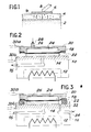
- FIG. 1 there is shown the gate of a transistor of an integrated MOS element. It comprises a layer 2 consisting of a doped semiconductor, an oxide layer 4 in which ionized impurities are mobile, and a metal layer 6.
- An electrical contact means 8 consisting for example of an electrical tip allows to bring the metal layer 6 to an electrical potential. By bringing the semiconductor layer 2 to another potential, it is then possible to plot the electrical capacitance-voltage characteristics and the operation of putting under con electric trestle of the integrated circuit area located to the right of the metal layer 6.
- the temperature constraint has the effect of activating the ionized impurities 9.
- the movement of these ionized impurities 9 is oriented by the electric voltage constraint.
- the direction of movement of the ionized impurities 9, represented in the figure by arrows, is arbitrary. It depends on the direction of the electric field prevailing in the oxide layer 4, that is to say on the sign of the applied electric voltage constraint, and it depends on the sign of the mobile electric charges.
- FIG 2 there is shown an embodiment of the device according to the invention.
- This device comprises a plate support 10 provided with heating means 12 supporting a silicon plate 14 on which the integrated circuits to be tested have been inserted.
- the silicon plate 14 is fixed to the plate support 10 by suction by means of a pump (not shown) connected to a conduit 16 drilled in the plate support 10.
- the entire device is under atmospheric pressure .
- the stressing of temperature of the silicon wafer 14 is done via the thermally conductive plate support 10 provided with a heating means 12.
- the stressing of electric voltage is done by means of two electric conductors 30a and 30b, the first applying via the housing 20 and the conductive membrane 18 a potential on the upper face of the silicon plate 14, the second applying a potential via the electrically conductive plate support 10 on the rear face of the silicon plate 14.
- the rear face of the silicon plate 14 is optionally treated to favor better electrical conductivity. So that the conductive membrane 18 correctly transmits the potential which is applied to it to the upper face of the silicon plate 14, it must be supported on this silicon plate 14. This is done in the case of this FIG.
- the membrane conductive 18 is placed on a housing 20 forming an inverted U.
- an overpressure is created by supplying compressed air through a channel 28 passing through an orifice 26 of the housing 20.
- An overpressure of a few tenths of a bar is sufficient if the device is under atmospheric pressure to achieve the bearing force of the conductive membrane 18 on the silicon wafer 14.
- the part 22 of the housing 20 which holds the conductive membrane 18 is slightly set back from the plane of the conductive membrane 18 to avoid contact with the heating plate support 10.
- FIG 3 there is shown another embodiment of the device according to the invention.
- This device comprises, as in the previous figure, a plate support 10 provided with a heating means 12 on which is deposited the silicon plate 14 containing the integrated circuits to be tested, this plate being fixed on the plate support 10 by suction by means of a pump connected to the conduit 16.
- the conductive membrane 18 is fixed, as in the previous figure, on a housing 20 in the shape of an inverted U provided with an orifice 26.
- the cavity 24 is therefore at the same pressure than the whole device.
- we will therefore create a depression on the side of the face of the conductive membrane 18 in contact with the silicon plate 14 relative to the other face of the conductive membrane 18.
- a seal 32 is used which encircles the silicon plate 14.
- This seal 32 can for example be toroidal. It rests on the plate support 10 and supports the part 22 of the housing 20.
- a conduit 34, drilled in the plate support 10, is connected on the one hand to the space encircled by the seal 32 and on the other hand to a vacuum pump (not shown), the implementation of which allows the desired vacuum to be achieved.
- a vacuum of a few tenths of a bar is sufficient if the cavity 24 of the housing 20 is at atmospheric pressure.
- the pressure in the conduit 34 must however be greater than that prevailing in the conduit 16 so that the fixing of the silicon plate 14 is ensured.
- the conductive membrane 18 can be made up of a thin metal sheet such as for example stainless steel, or it can be made up of an insulating sheet, for example of the Kapton type or Milar, covered with a conductive layer, for example aluminum or copper. In the second case, and if only one of the faces of the conductive membrane 18 is covered with a conductive layer, this face is electrically connected to the housing 20 so that the potential provided by the conductor 30a on the housing 20 is transmitted to it.
Landscapes
- Engineering & Computer Science (AREA)
- General Engineering & Computer Science (AREA)
- Physics & Mathematics (AREA)
- General Physics & Mathematics (AREA)
- Testing Or Measuring Of Semiconductors Or The Like (AREA)
- Testing Of Individual Semiconductor Devices (AREA)
- Solid State Image Pick-Up Elements (AREA)
Applications Claiming Priority (2)
| Application Number | Priority Date | Filing Date | Title |
|---|---|---|---|
| FR8303046 | 1983-02-24 | ||
| FR8303046A FR2541779B1 (fr) | 1983-02-24 | 1983-02-24 | Dispositif de controle des charges electriques mobiles dans un circuit integre en technologie mos |
Publications (2)
| Publication Number | Publication Date |
|---|---|
| EP0117810A1 true EP0117810A1 (de) | 1984-09-05 |
| EP0117810B1 EP0117810B1 (de) | 1987-05-06 |
Family
ID=9286229
Family Applications (1)
| Application Number | Title | Priority Date | Filing Date |
|---|---|---|---|
| EP84400338A Expired EP0117810B1 (de) | 1983-02-24 | 1984-02-17 | Anordnung zum Überwachen von beweglichen elektrischen Ladungen in einem in MOS Technologie ausgeführten integrierten Schaltkreis |
Country Status (5)
| Country | Link |
|---|---|
| US (1) | US4672313A (de) |
| EP (1) | EP0117810B1 (de) |
| JP (1) | JPS59163833A (de) |
| DE (1) | DE3463573D1 (de) |
| FR (1) | FR2541779B1 (de) |
Families Citing this family (5)
| Publication number | Priority date | Publication date | Assignee | Title |
|---|---|---|---|---|
| US4891584A (en) * | 1988-03-21 | 1990-01-02 | Semitest, Inc. | Apparatus for making surface photovoltage measurements of a semiconductor |
| US4839587A (en) * | 1988-03-29 | 1989-06-13 | Digital Equipment Corporation | Test fixture for tab circuits and devices |
| GB2302458A (en) * | 1995-06-14 | 1997-01-15 | Ibm | Printed circuit testing apparatus |
| US6570374B1 (en) * | 2000-06-23 | 2003-05-27 | Honeywell International Inc. | Vacuum chuck with integrated electrical testing points |
| US20070068567A1 (en) * | 2005-09-23 | 2007-03-29 | Rubin Leonid B | Testing apparatus and method for solar cells |
Citations (1)
| Publication number | Priority date | Publication date | Assignee | Title |
|---|---|---|---|---|
| US4340860A (en) * | 1980-05-19 | 1982-07-20 | Trigon | Integrated circuit carrier package test probe |
Family Cites Families (4)
| Publication number | Priority date | Publication date | Assignee | Title |
|---|---|---|---|---|
| US3405361A (en) * | 1964-01-08 | 1968-10-08 | Signetics Corp | Fluid actuable multi-point microprobe for semiconductors |
| US3596228A (en) * | 1969-05-29 | 1971-07-27 | Ibm | Fluid actuated contactor |
| US3949295A (en) * | 1974-03-20 | 1976-04-06 | Western Electric Company, Inc. | Apparatus for retaining articles in an array for testing |
| US3979671A (en) * | 1975-03-06 | 1976-09-07 | International Business Machines Corporation | Test fixture for use in a high speed electronic semiconductor chip test system |
-
1983
- 1983-02-24 FR FR8303046A patent/FR2541779B1/fr not_active Expired
-
1984
- 1984-02-16 US US06/580,840 patent/US4672313A/en not_active Expired - Fee Related
- 1984-02-17 DE DE8484400338T patent/DE3463573D1/de not_active Expired
- 1984-02-17 EP EP84400338A patent/EP0117810B1/de not_active Expired
- 1984-02-24 JP JP59032759A patent/JPS59163833A/ja active Pending
Patent Citations (1)
| Publication number | Priority date | Publication date | Assignee | Title |
|---|---|---|---|---|
| US4340860A (en) * | 1980-05-19 | 1982-07-20 | Trigon | Integrated circuit carrier package test probe |
Non-Patent Citations (2)
| Title |
|---|
| IBM TECHNICAL DISCLOSURE BULLETIN, vol. 14, no. 6, novembre 1971, pages 1924-1925, Armonk, US * |
| IBM TECHNICAL DISCLOSURE BULLETIN, vol. 16, no. 2, juillet 1973, pages 692-693, Armonk, US * |
Also Published As
| Publication number | Publication date |
|---|---|
| EP0117810B1 (de) | 1987-05-06 |
| FR2541779A1 (fr) | 1984-08-31 |
| FR2541779B1 (fr) | 1985-06-07 |
| DE3463573D1 (en) | 1987-06-11 |
| JPS59163833A (ja) | 1984-09-14 |
| US4672313A (en) | 1987-06-09 |
Similar Documents
| Publication | Publication Date | Title |
|---|---|---|
| US20120161253A1 (en) | Gas sensor and manufacturing method thereof | |
| FR2566181A1 (fr) | Procede d'autopositionnement d'une ligne d'interconnexion sur un trou de contact electrique d'un circuit integre | |
| CA1078528A (fr) | Procede de fabrication de semi-conducteurs de puissance a contacts presses | |
| FR2745637A1 (fr) | Dispositif capteur chimique a semiconducteur et procede de formation d'un thermocouple pour ce dispositif | |
| EP0117810B1 (de) | Anordnung zum Überwachen von beweglichen elektrischen Ladungen in einem in MOS Technologie ausgeführten integrierten Schaltkreis | |
| FR2786564A1 (fr) | Capteur de pression a membrane comportant du carbure de silicium et procede de fabrication | |
| FR2664979A1 (fr) | Micro-capteur de pression. | |
| EP0557216B1 (de) | Druckmikrosensor | |
| WO2001042742A1 (fr) | Emetteur et recepteur acoustiques integres, et procede de fabrication correspondant | |
| EP0011694B1 (de) | Verfahren und Vorrichtung zum reversiblen Einstellen elektrischer Parameter eines Stromkreises | |
| FR2629593A1 (fr) | Capteur pour la mesure capacitive de la pression dans des gaz | |
| GB2085168A (en) | Semiconductor gas sensor | |
| EP3455637B1 (de) | Vorgespannter vibrierender beschleunigungsmesser | |
| FR2718286A1 (fr) | Procédé d'attaque de tranches de semi-conducteur. | |
| FR2535458A1 (fr) | Capteur de pression et de temperature | |
| FR2812969A1 (fr) | Capteur micro-usine avec soudure electrolytique et procede de fabrication | |
| EP0080402B1 (de) | Vorrichtung zur Ermittlung einer Ionenkonzentration und Anwendung zur pH-Messung | |
| FR2645970A1 (fr) | Micromagnetometre a detection capacitive | |
| FR2465231A1 (fr) | Tete de mesure de microcircuits, et appareil de mesure comportant une telle tete | |
| JPH07162019A (ja) | 半導体圧力センサ | |
| FR2616542A1 (fr) | Procede de fabrication collective de capteurs de pression capacitifs | |
| FR2749694A1 (fr) | Procede et appareil pour exciter des cathodes a emission de champ | |
| JP3159530B2 (ja) | 誘電特性測定方法 | |
| FR3158794A1 (fr) | Dispositif d’analyse de gaz | |
| BE711537A (de) |
Legal Events
| Date | Code | Title | Description |
|---|---|---|---|
| PUAI | Public reference made under article 153(3) epc to a published international application that has entered the european phase |
Free format text: ORIGINAL CODE: 0009012 |
|
| AK | Designated contracting states |
Designated state(s): CH DE GB IT LI NL |
|
| 17P | Request for examination filed |
Effective date: 19850225 |
|
| 17Q | First examination report despatched |
Effective date: 19860527 |
|
| GRAA | (expected) grant |
Free format text: ORIGINAL CODE: 0009210 |
|
| AK | Designated contracting states |
Kind code of ref document: B1 Designated state(s): CH DE GB IT LI NL |
|
| REF | Corresponds to: |
Ref document number: 3463573 Country of ref document: DE Date of ref document: 19870611 |
|
| ITF | It: translation for a ep patent filed | ||
| RAP2 | Party data changed (patent owner data changed or rights of a patent transferred) |
Owner name: COMMISSARIAT A L'ENERGIE ATOMIQUE |
|
| NLT2 | Nl: modifications (of names), taken from the european patent patent bulletin |
Owner name: COMMISSARIAT A L'ENERGIE ATOMIQUE TE PARIJS, FRANK |
|
| PLBE | No opposition filed within time limit |
Free format text: ORIGINAL CODE: 0009261 |
|
| STAA | Information on the status of an ep patent application or granted ep patent |
Free format text: STATUS: NO OPPOSITION FILED WITHIN TIME LIMIT |
|
| 26N | No opposition filed | ||
| PGFP | Annual fee paid to national office [announced via postgrant information from national office to epo] |
Ref country code: DE Payment date: 19890123 Year of fee payment: 6 |
|
| PGFP | Annual fee paid to national office [announced via postgrant information from national office to epo] |
Ref country code: CH Payment date: 19890221 Year of fee payment: 6 |
|
| ITTA | It: last paid annual fee | ||
| PGFP | Annual fee paid to national office [announced via postgrant information from national office to epo] |
Ref country code: NL Payment date: 19890228 Year of fee payment: 6 Ref country code: GB Payment date: 19890228 Year of fee payment: 6 |
|
| PG25 | Lapsed in a contracting state [announced via postgrant information from national office to epo] |
Ref country code: GB Effective date: 19900217 |
|
| PG25 | Lapsed in a contracting state [announced via postgrant information from national office to epo] |
Ref country code: LI Effective date: 19900228 Ref country code: CH Effective date: 19900228 |
|
| PG25 | Lapsed in a contracting state [announced via postgrant information from national office to epo] |
Ref country code: NL Effective date: 19900901 |
|
| NLV4 | Nl: lapsed or anulled due to non-payment of the annual fee | ||
| GBPC | Gb: european patent ceased through non-payment of renewal fee | ||
| REG | Reference to a national code |
Ref country code: CH Ref legal event code: PL |
|
| PG25 | Lapsed in a contracting state [announced via postgrant information from national office to epo] |
Ref country code: DE Effective date: 19901101 |