EP0102734A2 - Reines grünes Licht emittierende Dioden und Verfahren zu deren Herstellung - Google Patents
Reines grünes Licht emittierende Dioden und Verfahren zu deren Herstellung Download PDFInfo
- Publication number
- EP0102734A2 EP0102734A2 EP83304315A EP83304315A EP0102734A2 EP 0102734 A2 EP0102734 A2 EP 0102734A2 EP 83304315 A EP83304315 A EP 83304315A EP 83304315 A EP83304315 A EP 83304315A EP 0102734 A2 EP0102734 A2 EP 0102734A2
- Authority
- EP
- European Patent Office
- Prior art keywords
- melt
- pure
- light emitting
- green light
- gap
- Prior art date
- Legal status (The legal status is an assumption and is not a legal conclusion. Google has not performed a legal analysis and makes no representation as to the accuracy of the status listed.)
- Granted
Links
Images



Classifications
-
- H—ELECTRICITY
- H10—SEMICONDUCTOR DEVICES; ELECTRIC SOLID-STATE DEVICES NOT OTHERWISE PROVIDED FOR
- H10H—INORGANIC LIGHT-EMITTING SEMICONDUCTOR DEVICES HAVING POTENTIAL BARRIERS
- H10H20/00—Individual inorganic light-emitting semiconductor devices having potential barriers, e.g. light-emitting diodes [LED]
- H10H20/80—Constructional details
- H10H20/81—Bodies
- H10H20/822—Materials of the light-emitting regions
- H10H20/824—Materials of the light-emitting regions comprising only Group III-V materials, e.g. GaP
-
- H—ELECTRICITY
- H10—SEMICONDUCTOR DEVICES; ELECTRIC SOLID-STATE DEVICES NOT OTHERWISE PROVIDED FOR
- H10H—INORGANIC LIGHT-EMITTING SEMICONDUCTOR DEVICES HAVING POTENTIAL BARRIERS
- H10H20/00—Individual inorganic light-emitting semiconductor devices having potential barriers, e.g. light-emitting diodes [LED]
- H10H20/01—Manufacture or treatment
- H10H20/011—Manufacture or treatment of bodies, e.g. forming semiconductor layers
- H10H20/013—Manufacture or treatment of bodies, e.g. forming semiconductor layers having light-emitting regions comprising only Group III-V materials
Definitions
- This invention relates to pure green light emitting diodes with high brightness which emit pure-green light clearly distinguishable from yellow-green light, and a method of manufacturing the same.
- Visible light emitting diodes are now being used as most of display devices.
- gallium phosphide (GaP) LED's can emit light with either of three kinds of color -- red, yellow-green and pure green -- by using a GaP substrate as a starting material. These LED's are widely used because of good characteristics and low cost.
- the pure green GaP LED's have lower brightness and inferior hue as compared with those of red and yellow-green GaP LED's. It is important to improve the above-mentioned characteristics in order to use GaP LED's as display devices.
- the peak emission wavelength of GaP pure-green LED's is about 555 nm.
- the conventional process of forming the LED's is through a growth of n-type and p-type epitaxial layers on an n-type GaP substrate by liquid phase method.
- the method of liquid phase epitaxial growth is roughly classified into the temperature difference method and the gradual cooling method.
- the former method is superior to the latter on the point of the quality of crystallization, but the control of temperature difference is difficult.
- the gradual cooling method is more favorable in view of mass production, and applied to the production of cheap LED's.
- In the formation of an epitaxial layer by the gradual cooling method if the n-type layer and p-type layer are grown from different melts by using slide boat, mechanical damages appear on the junction interface.
- GaP pure green LED's emit light either from n-type or p-type layer.
- the emission of pure green light occurs in the vicinity of the band gap of GaP and hence the self- absorption is negligible. Therefore, light emission from the p-type layer which is nearer to the LED surface than the n-type layer can have higher efficiency of external light emission.
- GaP pure green LED's are formed by the usual over- compensation method, donor impurities existing with high concentration in the p-type layer disturb the light emission. Thus, most of the GaP pure green LED's tend to be low-brightness emission LED's.
- the first objective of this invention is to realize GaP pure green LED's with high brightness and excellent hue in spite of using an epitaxial layer grown by the overcompensation method.
- the second objective of this invention is to provide a method of manufacturing the above-mentioned-GaP pure-green LED's.
- the third objective of this invention is to provide GaP pure-green LED's with high brightness and excellent hue, which enable the use of overcompensation method suitable for mass production.
- a further objective of this invention is to realize GaP pure-green LED's with clear contrast of hue with the yellow-green LED's thereby to extend the application range of GaP LED's for displays, etc.
- the structure of pure-green LED's of this invention is as follows. On an n-type GaP substrate, another GaP epitaxial layer is formed with the same conduction type as that of the substrate. A p-type GaP epitaxial layer is formed on the above GaP epitaxial layer by overcompensation liquid phase epitaxial method.
- the average donor concentration in the p-type epitaxial layer is set at a value less than or equal to 5 x 10 16 c m - 3
- This structure ensures emission of pure-green light with high brightness, in which the component of yellow light emission is suppressed.
- the n-type GaP epitaxial layer is formed, and subsequently acceptor impurities are supplied to this melt to compensate the donor impurities by using one melt.
- the ambient atmosphere of the melt is kept at a reduced pressure for a prescribed period, where the volatilization process of part of the donor impurities from the melt is undertaken. This process ensures to reduce the donor concnetration in the p-type GaP epitaxial layer less than or equal to 5 x 10 16 cm -3 .
- Fig. 1 showing the cross-section of the structure of a GaP pure-green LED's according to one embodiment of this invention
- 1 denotes an n-type GaP substrate
- 2 an n-type GaP epitaxial layer grown by the gradual cooling method with use of a melt containing sulphur (S) as donor impurities
- 3 a p-type GaP epitaxial layer with average donor concentration less than or equal to 5 x 10 16 cm- 3 .
- the latter p-type layer is grown from a melt which was used for the growth of the n-type GaP epitaxial layer and in which zinc (Zn) is added as acceptor impurities to compensate S.
- Fig. 2 is a diagram showing the method for manufacturing GaP pure-green LED shown in Fig. 1.
- a vessel 6 of melt having a GaP melt 5 therein is disposed on a boat 4 for accomodating a GaP substrate 1 which is serving as the starting material.
- This melt contains donor impurities S by 3 x 10- 5 mol% relative to Ga.
- the melt is gradually cooled from 1000°C to 900°C at a cooling rate of 1°C/min. to grow an n-type GaP epitaxial layer 2. Cooling is stopped at 900°C at which the process of growing the n-type GaP epitaxial layer 2 is finished. Then, the temperature of the melt is kept at 900°C.
- the internal ambience of the growth apparatus is maintained at a reduced pressure of 0.05 Torr. so that S in the melt is volatilized from the melt as shown by solid arrows in the figure. Thereafter, acceptor impurities Zn are supplied as vapor phase as shown by dotted arrows in the figure.
- the melt is then gradually cooled from 900°C to 800°C at a cooling rate of 1°C/min., whereby an P-type GaP epitaxial layer 3 is grown.
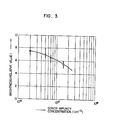
- Fig. 3 shows the relation between the brightness and the average donor concentration in the p-type GaP epitaxial layer of Ga pure-green LED's formed in the above-mentioned process.
- the brightness increases.
- the brightness exceeds a relative value of 7 above which high brightness LED's can be realized.
- the average donor concentration shown in the figure decreases with increasing the setting time of the state with the reduced pressure.
- the conduction type did not invert to p-type.
- the period of reduced pressure was longer than 3 hours, phosphor (P) was also volatilized from the melt. This causes unsaturation of melt, and the n-type epitaxial layer already grown dissolves into the melt. Therefore, the donor concentration may not be reduced below the value indicated in the figure.
- Fig. 4 shows the distribution of impurity concentration in the GaP pure-green LED's formed through the above-mentioned menufacturing process, where the process of reduced pressure is kept for 3 hours.
- Regions 1, 2 and 3 correspond to the regions 1, 2 and 3 of the structure shown in Fig. 1, respectively.
- A denotes the donor (impurity) concentration
- wnile B denotes the acceptor (impurity) cocentration.
- the measured value of the average donor concentration in the p-type GaP epitaxial layer 3 of the GaP pure green LED's was 3 x 10 16 cm- 3 .
- the average donor concentration in the p-type GaP epitaxial layer of GaP pure-green LED's formed by setting the period of reduced pressure 1 and 2 hours were 1.5 x 10 cm -3 and 7 x 10 cm -3 , respectively.
- Fig. 5 shows experimental data of emission spectrum dependent upon the period of reduced pressure, i.e., the variation of the spectrum of light emission of GaP pure-green LED's, when the period of reduced pressure was varied from 1 to 3 hours in the manufacturing process of GaP pure-green LED's.
- C, D and E correspond to the characteristics with the period of reduced pressure set as 1, 2 and 3 hours, respectively. There is seen a tendency such that the emission of yellow light near 570 nm lessens or disappears to be invisible as the period of reduced pressure increases.
- Characteristic E of GaP pure green LED's satisfying the condition of average donor concentration of less than or equal to 5 x 10 16 cm -3 in p-type GaP epitaxial layer with setting of the period of reduced pressure as 3 hours has little emission of yellow light near 570 nm. Therefore, emission of pure-green light showing a clear contrast with the light emitted by GaP yellow-green LED's could be obtained.
- GaP pure-green LED's of this invention with such a structure as explained in conjunction with the embodiment can be manufactured by the basic process of gradual cooling combining the conventional overcompensation method with addition of only one step with a reduced pressure, and hence is favorable in view of mass production.
- This GaP pure-green LED's have a characteristics of emitting green light with high brightness and excellent hue easily distinguishable from yellow-green light. Since GaP pure-green LED's of this invention is suitable for mass production, cost reduction can be expected. The effect is that supply of GaP pure-green LED's can be made cheaply. Furthermore, since GaP pure-green LED's of this invention have excellent hue, it can contribute to realize three kinds of LED's emitting red, yellow-green and pure green light with high brightness from a raw GaP material. Range of application of GaP LED's to the field of displays is thus extended.
Landscapes
- Led Devices (AREA)
- Liquid Deposition Of Substances Of Which Semiconductor Devices Are Composed (AREA)
Applications Claiming Priority (2)
| Application Number | Priority Date | Filing Date | Title |
|---|---|---|---|
| JP132735/82 | 1982-07-28 | ||
| JP57132735A JPS5922376A (ja) | 1982-07-28 | 1982-07-28 | 純緑色発光ダイオ−ドおよびその製造方法 |
Publications (3)
| Publication Number | Publication Date |
|---|---|
| EP0102734A2 true EP0102734A2 (de) | 1984-03-14 |
| EP0102734A3 EP0102734A3 (en) | 1985-06-12 |
| EP0102734B1 EP0102734B1 (de) | 1990-03-14 |
Family
ID=15088365
Family Applications (1)
| Application Number | Title | Priority Date | Filing Date |
|---|---|---|---|
| EP83304315A Expired - Lifetime EP0102734B1 (de) | 1982-07-28 | 1983-07-26 | Reines grünes Licht emittierende Dioden und Verfahren zu deren Herstellung |
Country Status (5)
| Country | Link |
|---|---|
| US (1) | US4965644A (de) |
| EP (1) | EP0102734B1 (de) |
| JP (1) | JPS5922376A (de) |
| CA (1) | CA1237514A (de) |
| DE (1) | DE3381338D1 (de) |
Cited By (4)
| Publication number | Priority date | Publication date | Assignee | Title |
|---|---|---|---|---|
| US5032539A (en) * | 1988-07-08 | 1991-07-16 | Kabushiki Kaisha Toshiba | Method of manufacturing green light emitting diode |
| EP0584599A1 (de) * | 1992-08-28 | 1994-03-02 | Siemens Aktiengesellschaft | Leuchtdiode |
| EP0631330A3 (de) * | 1993-05-31 | 1995-03-22 | Shinetsu Handotai Kk | GaP-Substrat einer pur grünes licht emittierenden Vorrichtung. |
| US5851850A (en) * | 1992-07-31 | 1998-12-22 | Shin-Etsu Handotai Co., Ltd. | Method for fabricating a gap type semiconductor substrate of red light emitting devices |
Families Citing this family (32)
| Publication number | Priority date | Publication date | Assignee | Title |
|---|---|---|---|---|
| US6590502B1 (en) | 1992-10-12 | 2003-07-08 | 911Ep, Inc. | Led warning signal light and movable support |
| JPH06219279A (ja) * | 1993-01-27 | 1994-08-09 | Sankosha:Kk | 多灯形色灯式信号機 |
| JP3163217B2 (ja) * | 1994-05-31 | 2001-05-08 | シャープ株式会社 | 発光ダイオード及びその製造方法 |
| JPH10173218A (ja) * | 1996-12-16 | 1998-06-26 | Showa Denko Kk | GaP純緑色発光ダイオード用エピタキシャルウェーハ |
| GB2330679B (en) | 1997-10-21 | 2002-04-24 | 911 Emergency Products Inc | Warning signal light |
| US6462669B1 (en) | 1999-04-06 | 2002-10-08 | E. P . Survivors Llc | Replaceable LED modules |
| US6380865B1 (en) | 1999-04-06 | 2002-04-30 | 911 Emergency Products, Inc. | Replacement led lamp assembly and modulated power intensity for light source |
| US6614359B2 (en) | 1999-04-06 | 2003-09-02 | 911 Emergency Products, Inc. | Replacement led lamp assembly and modulated power intensity for light source |
| US6700502B1 (en) | 1999-06-08 | 2004-03-02 | 911Ep, Inc. | Strip LED light assembly for motor vehicle |
| US6705745B1 (en) * | 1999-06-08 | 2004-03-16 | 911Ep, Inc. | Rotational led reflector |
| WO2000074972A1 (en) | 1999-06-08 | 2000-12-14 | 911 Emergency Products, Inc. | Led light stick assembly |
| US6367949B1 (en) | 1999-08-04 | 2002-04-09 | 911 Emergency Products, Inc. | Par 36 LED utility lamp |
| US6623151B2 (en) | 1999-08-04 | 2003-09-23 | 911Ep, Inc. | LED double light bar and warning light signal |
| US6547410B1 (en) | 2000-07-28 | 2003-04-15 | 911 Emergency Products, Inc. | LED alley/take-down light |
| WO2001095673A1 (en) | 2000-06-06 | 2001-12-13 | 911 Emergency Products, Inc. | Led compensation circuit |
| US7439847B2 (en) * | 2002-08-23 | 2008-10-21 | John C. Pederson | Intelligent observation and identification database system |
| US8188878B2 (en) | 2000-11-15 | 2012-05-29 | Federal Law Enforcement Development Services, Inc. | LED light communication system |
| WO2002041276A2 (en) * | 2000-11-15 | 2002-05-23 | Snowy Village, Inc. | Led warning light and communication system |
| JP4080843B2 (ja) | 2002-10-30 | 2008-04-23 | 株式会社東芝 | 不揮発性半導体記憶装置 |
| JP4412963B2 (ja) | 2003-10-10 | 2010-02-10 | 旭有機材工業株式会社 | バルブ用樹脂製部材 |
| US9294198B2 (en) | 2007-05-24 | 2016-03-22 | Federal Law Enforcement Development Services, Inc. | Pulsed light communication key |
| WO2008148039A1 (en) | 2007-05-24 | 2008-12-04 | Federal Law Enforcement Development Services, Inc. | Led light communication system |
| US9100124B2 (en) | 2007-05-24 | 2015-08-04 | Federal Law Enforcement Development Services, Inc. | LED Light Fixture |
| US9455783B2 (en) | 2013-05-06 | 2016-09-27 | Federal Law Enforcement Development Services, Inc. | Network security and variable pulse wave form with continuous communication |
| US9258864B2 (en) | 2007-05-24 | 2016-02-09 | Federal Law Enforcement Development Services, Inc. | LED light control and management system |
| US9414458B2 (en) | 2007-05-24 | 2016-08-09 | Federal Law Enforcement Development Services, Inc. | LED light control assembly and system |
| US11265082B2 (en) | 2007-05-24 | 2022-03-01 | Federal Law Enforcement Development Services, Inc. | LED light control assembly and system |
| US8890773B1 (en) | 2009-04-01 | 2014-11-18 | Federal Law Enforcement Development Services, Inc. | Visible light transceiver glasses |
| US8543505B2 (en) | 2011-01-14 | 2013-09-24 | Federal Law Enforcement Development Services, Inc. | Method of providing lumens and tracking of lumen consumption |
| US9265112B2 (en) | 2013-03-13 | 2016-02-16 | Federal Law Enforcement Development Services, Inc. | LED light control and management system |
| US20150198941A1 (en) | 2014-01-15 | 2015-07-16 | John C. Pederson | Cyber Life Electronic Networking and Commerce Operating Exchange |
| US20170046950A1 (en) | 2015-08-11 | 2017-02-16 | Federal Law Enforcement Development Services, Inc. | Function disabler device and system |
Family Cites Families (8)
| Publication number | Priority date | Publication date | Assignee | Title |
|---|---|---|---|---|
| US3870575A (en) * | 1972-03-21 | 1975-03-11 | Sony Corp | Fabricating a gallium phosphide device |
| NL7315451A (de) * | 1972-11-16 | 1974-05-20 | ||
| US4001056A (en) * | 1972-12-08 | 1977-01-04 | Monsanto Company | Epitaxial deposition of iii-v compounds containing isoelectronic impurities |
| US3931631A (en) * | 1973-07-23 | 1976-01-06 | Monsanto Company | Gallium phosphide light-emitting diodes |
| US4101920A (en) * | 1975-01-29 | 1978-07-18 | Sony Corporation | Green light emitting diode |
| JPS5439573A (en) * | 1977-09-05 | 1979-03-27 | Toshiba Corp | Compound semiconductor device |
| DE2843983C2 (de) * | 1977-10-07 | 1983-09-15 | Tokyo Shibaura Denki K.K., Kawasaki, Kanagawa | Verfahren zum Herstellen einer Grünlicht emittierenden GaP-Lumineszenzdiode |
| JPS5596629A (en) * | 1979-01-17 | 1980-07-23 | Matsushita Electric Ind Co Ltd | Method of epitaxially growing in liquid phase |
-
1982
- 1982-07-28 JP JP57132735A patent/JPS5922376A/ja active Pending
-
1983
- 1983-07-26 EP EP83304315A patent/EP0102734B1/de not_active Expired - Lifetime
- 1983-07-26 CA CA000433193A patent/CA1237514A/en not_active Expired
- 1983-07-26 DE DE8383304315T patent/DE3381338D1/de not_active Expired - Lifetime
-
1985
- 1985-11-12 US US06/797,756 patent/US4965644A/en not_active Expired - Lifetime
Cited By (5)
| Publication number | Priority date | Publication date | Assignee | Title |
|---|---|---|---|---|
| US5032539A (en) * | 1988-07-08 | 1991-07-16 | Kabushiki Kaisha Toshiba | Method of manufacturing green light emitting diode |
| US5851850A (en) * | 1992-07-31 | 1998-12-22 | Shin-Etsu Handotai Co., Ltd. | Method for fabricating a gap type semiconductor substrate of red light emitting devices |
| EP0584599A1 (de) * | 1992-08-28 | 1994-03-02 | Siemens Aktiengesellschaft | Leuchtdiode |
| US5614736A (en) * | 1992-08-28 | 1997-03-25 | Siemens Aktiengesellschaft | Gallium phosphate light emitting diode with zinc-doped contact |
| EP0631330A3 (de) * | 1993-05-31 | 1995-03-22 | Shinetsu Handotai Kk | GaP-Substrat einer pur grünes licht emittierenden Vorrichtung. |
Also Published As
| Publication number | Publication date |
|---|---|
| EP0102734A3 (en) | 1985-06-12 |
| JPS5922376A (ja) | 1984-02-04 |
| CA1237514A (en) | 1988-05-31 |
| DE3381338D1 (de) | 1990-04-19 |
| US4965644A (en) | 1990-10-23 |
| EP0102734B1 (de) | 1990-03-14 |
Similar Documents
| Publication | Publication Date | Title |
|---|---|---|
| US4965644A (en) | Pure green light emitting diodes and method of manufacturing the same | |
| US4671829A (en) | Manufacturing green light emitting diodes | |
| US6479312B1 (en) | Gallium phosphide luminescent device | |
| US4946801A (en) | Epitaxial wafer | |
| JPH09129927A (ja) | 青色発光素子 | |
| JP2001274454A (ja) | 発光ダイオード及びその製造方法 | |
| JPH07142764A (ja) | エピタキシャルウェーハの製造方法 | |
| US5032539A (en) | Method of manufacturing green light emitting diode | |
| KR19980070852A (ko) | 에피택시얼 웨이퍼 및 이의 제조방법과 휘도가 증가된 발광다이오드 | |
| JP2817577B2 (ja) | GaP純緑色発光素子基板 | |
| JP2924579B2 (ja) | 発光ダイオードの製造方法 | |
| JP3187279B2 (ja) | 赤外発光ダイオードおよびその製造方法 | |
| JP3624451B2 (ja) | 発光素子用GaPエピタキシャル基板 | |
| US5886369A (en) | Epitaxial wafer for GaP pure green light-emitting diode and GaP pure green light-emitting diode | |
| KR20010099146A (ko) | 후 열처리에 따른 산화아연 박막의 발광파장 조절방법 | |
| US6433365B1 (en) | Epitaxial wafer and light emitting diode | |
| JP3116495B2 (ja) | 発光ダイオードの製造方法 | |
| JP2000058904A (ja) | エピタキシャルウェハ及びその製造方法並びに発光ダイオード | |
| KR0177007B1 (ko) | 액상 에피택셜 성장법 | |
| KR100719915B1 (ko) | 산화아연을 이용한 단파장 발광소자 제조방법 | |
| KR100430615B1 (ko) | 적외선 발광 소자용 에피택셜 웨이퍼 | |
| KR940003435B1 (ko) | 발광소자 및 그 제조방법 | |
| JPS6013317B2 (ja) | 発光ダイオ−ドの製造方法 | |
| JPH08288546A (ja) | 発光ダイオード | |
| KR20010070679A (ko) | 후 열처리에 따른 단파장 산화아연 발광소자의 제조방법 |
Legal Events
| Date | Code | Title | Description |
|---|---|---|---|
| PUAI | Public reference made under article 153(3) epc to a published international application that has entered the european phase |
Free format text: ORIGINAL CODE: 0009012 |
|
| AK | Designated contracting states |
Designated state(s): DE FR GB |
|
| PUAL | Search report despatched |
Free format text: ORIGINAL CODE: 0009013 |
|
| AK | Designated contracting states |
Designated state(s): DE FR GB |
|
| 17P | Request for examination filed |
Effective date: 19851114 |
|
| 17Q | First examination report despatched |
Effective date: 19870520 |
|
| GRAA | (expected) grant |
Free format text: ORIGINAL CODE: 0009210 |
|
| AK | Designated contracting states |
Kind code of ref document: B1 Designated state(s): DE FR GB |
|
| REF | Corresponds to: |
Ref document number: 3381338 Country of ref document: DE Date of ref document: 19900419 |
|
| ET | Fr: translation filed | ||
| PLBE | No opposition filed within time limit |
Free format text: ORIGINAL CODE: 0009261 |
|
| STAA | Information on the status of an ep patent application or granted ep patent |
Free format text: STATUS: NO OPPOSITION FILED WITHIN TIME LIMIT |
|
| 26N | No opposition filed | ||
| REG | Reference to a national code |
Ref country code: GB Ref legal event code: 746 Effective date: 19960628 |
|
| PGFP | Annual fee paid to national office [announced via postgrant information from national office to epo] |
Ref country code: FR Payment date: 20010712 Year of fee payment: 19 |
|
| PGFP | Annual fee paid to national office [announced via postgrant information from national office to epo] |
Ref country code: DE Payment date: 20010716 Year of fee payment: 19 |
|
| PGFP | Annual fee paid to national office [announced via postgrant information from national office to epo] |
Ref country code: GB Payment date: 20010725 Year of fee payment: 19 |
|
| REG | Reference to a national code |
Ref country code: GB Ref legal event code: IF02 |
|
| PG25 | Lapsed in a contracting state [announced via postgrant information from national office to epo] |
Ref country code: GB Free format text: LAPSE BECAUSE OF NON-PAYMENT OF DUE FEES Effective date: 20020726 |
|
| PG25 | Lapsed in a contracting state [announced via postgrant information from national office to epo] |
Ref country code: DE Free format text: LAPSE BECAUSE OF NON-PAYMENT OF DUE FEES Effective date: 20030201 |
|
| GBPC | Gb: european patent ceased through non-payment of renewal fee |
Effective date: 20020726 |
|
| PG25 | Lapsed in a contracting state [announced via postgrant information from national office to epo] |
Ref country code: FR Free format text: LAPSE BECAUSE OF NON-PAYMENT OF DUE FEES Effective date: 20030331 |
|
| REG | Reference to a national code |
Ref country code: FR Ref legal event code: ST |