EP0103455A2 - Leistungsquellenschaltung - Google Patents
Leistungsquellenschaltung Download PDFInfo
- Publication number
- EP0103455A2 EP0103455A2 EP83305179A EP83305179A EP0103455A2 EP 0103455 A2 EP0103455 A2 EP 0103455A2 EP 83305179 A EP83305179 A EP 83305179A EP 83305179 A EP83305179 A EP 83305179A EP 0103455 A2 EP0103455 A2 EP 0103455A2
- Authority
- EP
- European Patent Office
- Prior art keywords
- power supply
- transistor
- external control
- voltage
- supply circuit
- Prior art date
- Legal status (The legal status is an assumption and is not a legal conclusion. Google has not performed a legal analysis and makes no representation as to the accuracy of the status listed.)
- Withdrawn
Links
Images




Classifications
-
- H—ELECTRICITY
- H03—ELECTRONIC CIRCUITRY
- H03F—AMPLIFIERS
- H03F1/00—Details of amplifiers with only discharge tubes, only semiconductor devices or only unspecified devices as amplifying elements
- H03F1/52—Circuit arrangements for protecting such amplifiers
-
- G—PHYSICS
- G05—CONTROLLING; REGULATING
- G05F—SYSTEMS FOR REGULATING ELECTRIC OR MAGNETIC VARIABLES
- G05F1/00—Automatic systems in which deviations of an electric quantity from one or more predetermined values are detected at the output of the system and fed back to a device within the system to restore the detected quantity to its predetermined value or values, i.e. retroactive systems
- G05F1/10—Regulating voltage or current
- G05F1/46—Regulating voltage or current wherein the variable actually regulated by the final control device is DC
- G05F1/468—Regulating voltage or current wherein the variable actually regulated by the final control device is DC characterised by reference voltage circuitry, e.g. soft start, remote shutdown
Definitions
- the present invention relates to a power supply circuit which can stepwisely change its stabilized output voltage in response to an external control signal.
- the power supply circuit in accordance with the present invention can be used, for example, for changing the voltage level applied to microwave amplifiers so as to change the amplification degree or for cutting off or restoring the stabilized output voltage applied to microwave amplifiers.
- Stabilizing power supply circuits are used for a wide range of applications.
- two stepwisely changeable stabilized power supplies are required: one for changing an amplification degree of a microwave amplifier, in the case of two microwave amplifiers being operated in parallel and different voltage supplies being applied to one of the amplifiers so as to detect inoperation of the other; and the other, for cutting off the stabilized power supply to a microwave amplifier when the amplifier is in an abnormal state and restoring the power supply when the amplifier returns to normal.
- a first way is to prepare two circuits, one providing a higher output voltage and the other providing a lower output voltage. As can be clearly understood, this has the disadvantages of higher manufacturing cost, greater size, and the need for a complicated switching circuit.
- a second way is to install parallel resistors in the circuit-and change these resistors in response to external conditions.
- This approach however, has the disadvantages of a slight loss of stability in voltage potentials during transition and the'need for a complicated switching circuit.
- a third approach is to use a variable resistor in the circuit and to vary the resitance by a manual or automatic changing means. This,however, results in less operability and may entail use of a considerably complex device when automatic changing is desired.
- the object of the present invention is to provide a power supply circuit which can provide a stabilized voltage which is reduced or cut off in response to an external control signal, by means of simple circuit technology.
- a power supply circuit comprising: an output transistor providing a stabilized output voltage; a control transistor controlling a base potential of the output transistor; an impedance means connected to a base of the control transistor such that the impedance means divides the stabilized voltage into parts, one of the said parts of the divided voltage being applied to the base of the control transistor; and characterized by a switching means which is turned on or off in response to an external control signal so as to vary a division ratio provided by the impedance means.
- a power supply circuit comprising; a stabilized voltage generating circuit including an output transistor stabilizing the voltage level; the circuit being characterized by a thyristor means connected to a base of the output transistor and which is triggered and becomes conductive when a first external control signal reaches a first predetermined value; and a switching means connected to the thyristor means in series and turned on when a second external control signal of a lower trigger level than the first external control signal reaches a second predetermined value; wherein the stabilized voltage is cut when the first external control signal reaches the first predetermined value and the stabilized voltage is restored when the second external control signal drops to the second predetermined value.
- FIG. 1 shows the prior art circuit.
- V. designates an input terminal, V out an output terminal, GND a grounded terminal, TR1 and TR2 transistors, Dl a zener diode, and Rl, R2, R3, and R4 resistors.
- Series-connected resistors R3 and R4 are inserted between the output terminal V out and the ground terminal GND.
- a base of the transistor TR2 At a point between resistors R3 and R4 is connected a base of the transistor TR2.
- An emitter of the transistor TR2 is connected to the zener diode Dl for generating a reference voltage, and a collector thereof is connected to a base of the transistor TRl. Therefore, the transistor TR2 becomes active when the voltage (potential) at the above connecting point, i.e., the base potential of the transistor TR2, becomes greater than the emitter potential of the transistor TR2 and exceeds a predetermined value.
- the transistor TR2 When the transistor TR2 is further activated and the conductivity thereof is increased, the base potential of the transistor TR1 becomes low and the conductivity of transistor TR1 is reduced, whereby the output voltage at the output terminal V out can be maintained low.
- the transistor TR2 becomes inactive.
- the conductivity of the transistor TR2 is reduced, the base potential of the transistor TR1 becomes high and the conductivity thereof becomes higher, whereby the output voltage at the output terminal V out can become high.
- Figure 2 shows a power supply circuit in accordance with an embodiment of the present invention.
- V in indicates an input terminal, V out an output terminal, GND a grounded terminal, V an external control input terminal, TRll to TR14 transistors, Dll a zener diode, Rll to R13 resistors, R14 a variable resistor, R15 to R17 resistors, Vl a voltage potential across resistor R13, and V2 a voltage potential across resistor R14.
- the transistor TR14 whose collector is connected to a sliding terminal of the variable resistor R14, is turned on or off in response to a signal on the external control input terminal V ext .
- the resistance between a base of the transistor TR12 and the grounded terminal GND is therefore changed, and the voltage V2 to be compared with a reference voltage produced by the zener diode Dll is changed.
- the operating point of the transistor TR12 is changed.
- the voltage at the output terminal V out may be changed to the high level or low level.
- Fig. 2 The output-voltage stabilizing operation in Fig. 2 is similar to that of the circuit in Fig. 1, so a detailed description will be omitted. Only the differences will be described below with reference to Figs. 3(A) to 3(C).
- Figure 3(A) shows an input voltage (V. ) characteristic which is approximately constant independent of time (t).
- Figure 3(B) shows two conditions of the signal on the external control input terminal V ext i.e., a logical low (LO) condition and a logical high (HI) condition.
- Figure 3(C) shows the output voltage at the terminal V out , which may change to high (Vl) or low (V2) in response to the signal on the external control input terminal V ext .
- the transistor TR13 is turned on and the transistor TR14 is turned off, whereby the resistance of the variable resistor R14 is selected to its maximum value. Therefore, the resultant output voltage at the terminal V out is a low stabilized voltage potential (V 2 in Fig. 3(C)) smaller than that when the signal on the external control input terminal V ext is zero.
- the operating point of the transistor TR12 which controls the on or off state of the output transistor TR11 stabilizing the output effective voltage, can be changed by changing the/resistance of the variable resistor R14 connected to the base of the transistor TR12.
- the change of the variable resistor R14 is effected by turning on or turning off the transistor TR14, whose collector is connected to the sliding terminal of the resistor R14, in response to the condition of the external control signal. Accordingly, the circuit shown in Fig. 2 outputs a high stabilized voltage or low stabilized voltage in response to the condition of the external control signal.
- the high stabilized voltage and the low stabilized voltage are defined by suitably setting circuit parameters.
- the high stabilized voltage is defined by arranging the position of the sliding terminal of the variable resistor R14.
- a circuit shown in Fig. 2 for a power supply of, for example, a microwave amplifier using a gallium-arsenic field effect transistor, enables the output signal level of the microwave amplifier to be easily changed from high to low, and vice versa, whereby the amplification degree of the microwave amplifier can be easily changed just by changing the level of the external control signal.
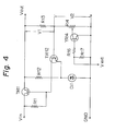
- Fig. 4 shows a modified embodiment of the circuit shown in Fig. 2.
- the circuit responsive to the signal on the external control signal terminal V ext is simplified.
- the fundamental operation is similar to that of the circuit shown in Fig. 2, except that the polarity of the external control signal is reverse that of the circuit of Fig. 2.
- V in represents an input terminal
- V out represents an output terminal
- a stabilizing power supply circuit SPS is similar to that in Fig. 1.
- the circuit shown in Fig. 5 further includes a thyristor SCR whose anode is connected to a base of the transistor TR11, a transistor TR21 whose collector is connected to a cathode of the thyristor and whose emitter is connected to a ground GND, a set of thermistors TH, incorporating a first thermistor TH1 and a second thermistor TH2, a zener diode D22 triggering the thyristor SCR in response to the second thermistor TH2, a zener diode D21 defining the voltage between the thermistor set TH and the ground GND, two variable resistors R23 and R24, and resistors R21 and R25.
- the above circuit may, for example, be employed for a microwave amplifier as a stabilized power supply circuit which cuts off the power supply when the temperature detected by the thermistor set TH exceeds a predetermined value and which restores the power supply when the temperature falls below another predetermined value.
- the load in Fig. 5- corresponds to the microwave amplifier and the thermistor set TH is attached to the casing of the amplifier so as to detect the temperature of the amplifier.
- a temperature Tl is defined as the threshold level which turns the transistor TR21 on or off.
- the base potential of the transistor TR21 is defined by means of the temperature Tl detected by the thermistor TH1 as well as circuit parameter of TH1 and R23.
- a temperature T2 is defined as the trigger level which ignites the thyristor SCR so as to make it conductive.
- the temperature T2 is higher than the temperature Tl. This is essential to obtain a deadband characteristic and to turn the thyristor SCR off.
- the temperature in the casing of the amplifier is lower than Tl and a rated output voltage (Vh i in Fig. 6(C) is applied to the amplifier as a load.
- the thyristor SCR is thereby, inhibited, and the transistor TR21 is turned off.
- the resistance of the thermistor set TH becomes low.
- the transistor TR21 is turned on due to the voltage at the connecting points of the thermistor TH1 and the variable resistor R23 (Fig. 6(B)).
- the thyristor SCR is triggered due to the voltage at the connecting point of the thermistor TH2 and the variable resistor R24.
- the base potential of the transistor TRll in stability power supply circuit SPS becomes low and the transistor T Rll is turned off, whereby the microwave amplifier is cut off from the power source (VLO in Fig. 6(C)).
- the temperature in the casing may drop.
- the transistor TR21 is turned off, whereby the thyristor SCR is turned off and the transistor TR11 is turned on. Therefore, the power supply to the microwave amplifier is_restored to the rated stabilized voltage level (V hi in Fig. 6(C)).
- the circuit shown in Fig. 5 provides a rated stabilized voltage or a low level voltage, which is substantially zero, depending on the load condition. It should be noted that the above circuit has a deadband characteristic due to the thermistor conditions. In other words, the circuit also provides two stabilized voltages in response to the conditions of the external control signals.
- the present invention has been described in reference to the above embodiments, it is not limited thereto except as defined in the claims.
- the thyristor SCR can be replaced by a triac.
- the thermistor can be replaced by another temperature sensor, such as a posistor (critical temperature resistor) which has a reverse characteristic to a thermistor.
Landscapes
- Engineering & Computer Science (AREA)
- Physics & Mathematics (AREA)
- Electromagnetism (AREA)
- General Physics & Mathematics (AREA)
- Radar, Positioning & Navigation (AREA)
- Automation & Control Theory (AREA)
- Power Engineering (AREA)
- Continuous-Control Power Sources That Use Transistors (AREA)
- Electronic Switches (AREA)
Applications Claiming Priority (4)
| Application Number | Priority Date | Filing Date | Title |
|---|---|---|---|
| JP15770082A JPS5947618A (ja) | 1982-09-10 | 1982-09-10 | 電源回路 |
| JP157700/82 | 1982-09-10 | ||
| JP172349/82 | 1982-09-29 | ||
| JP57172349A JPS5961225A (ja) | 1982-09-29 | 1982-09-29 | 電子回路 |
Publications (2)
| Publication Number | Publication Date |
|---|---|
| EP0103455A2 true EP0103455A2 (de) | 1984-03-21 |
| EP0103455A3 EP0103455A3 (de) | 1984-07-11 |
Family
ID=26485063
Family Applications (1)
| Application Number | Title | Priority Date | Filing Date |
|---|---|---|---|
| EP83305179A Withdrawn EP0103455A3 (de) | 1982-09-10 | 1983-09-06 | Leistungsquellenschaltung |
Country Status (3)
| Country | Link |
|---|---|
| US (1) | US4538102A (de) |
| EP (1) | EP0103455A3 (de) |
| CA (1) | CA1207384A (de) |
Cited By (4)
| Publication number | Priority date | Publication date | Assignee | Title |
|---|---|---|---|---|
| EP0176708A1 (de) * | 1984-08-10 | 1986-04-09 | Siemens Aktiengesellschaft | Schaltungsanordnung zur Temperatursicherung mit Hysterese |
| EP0345303A4 (de) * | 1987-03-09 | 1990-01-08 | Motorola Inc | Adaptiver thermischer schutz mittels fernmessung für einen leistungsverstärker. |
| FR2667960A1 (fr) * | 1990-10-16 | 1992-04-17 | Siemens Automotive Sa | Dispositif d'etablissement d'un courant dans une partie analogique d'un circuit integre logique et analogique. |
| EP0576772A1 (de) * | 1992-06-25 | 1994-01-05 | STMicroelectronics S.r.l. | Programmierbarer Ausgangsspannungsregler |
Families Citing this family (7)
| Publication number | Priority date | Publication date | Assignee | Title |
|---|---|---|---|---|
| JPH04259017A (ja) * | 1991-02-14 | 1992-09-14 | Brother Ind Ltd | 直流電源装置 |
| US5177431A (en) * | 1991-09-25 | 1993-01-05 | Astec International Ltd. | Linear programming circuit for adjustable output voltage power converters |
| US5430365A (en) * | 1993-07-02 | 1995-07-04 | Tandem Computers Incorporated | Power regulation for redundant battery supplies |
| US5712555A (en) * | 1996-02-13 | 1998-01-27 | Hughes Electronics | Voltage regulation for access cards |
| KR100208353B1 (ko) * | 1996-08-22 | 1999-07-15 | 윤종용 | 마이크로 컴퓨터의 전원회로 및 그 전원공급 제어방법 |
| TWI332136B (en) * | 2006-10-11 | 2010-10-21 | Chimei Innolux Corp | Voltage stabilizing circuit |
| EP2828721A4 (de) | 2012-03-22 | 2016-01-13 | Intel Corp | Vorrichtung, system und verfahren zur spannungspegelschaltung |
Family Cites Families (10)
| Publication number | Priority date | Publication date | Assignee | Title |
|---|---|---|---|---|
| US3480852A (en) * | 1967-10-20 | 1969-11-25 | Forbro Design Corp | Ambient and component temperature compensated voltage current regulator |
| GB1222751A (en) * | 1969-03-03 | 1971-02-17 | Comm Consultants Ltd | Stabilized d.c. power supply |
| US3643151A (en) * | 1969-09-17 | 1972-02-15 | Matsushita Electric Industrial Co Ltd | Overcurrent proof constant voltage |
| JPS5239717Y2 (de) * | 1972-04-14 | 1977-09-08 | ||
| US3866136A (en) * | 1973-04-23 | 1975-02-11 | Motorola Inc | Amplifier protection circuit |
| DE2409798B2 (de) * | 1974-03-01 | 1978-09-14 | Neumann Elektronik Gmbh, 4330 Muelheim | Kurzschluß- und Überlastungsschutzeinrichtung für einen mit Halbleiterelementen bestückten Verstärker |
| US4090123A (en) * | 1976-11-11 | 1978-05-16 | Forbro Design Corp. | Regulated power supply crow-bar protection |
| SU658544A1 (ru) * | 1977-03-09 | 1979-04-25 | Предприятие П/Я Р-6707 | Стабилизатор посто нного напр жени с защитой от перегрузок и коротких замыканий |
| EP0031987B1 (de) * | 1980-01-04 | 1986-04-16 | Fanuc Ltd. | Referenzspannungsquelle für eine geregelte Gleichspannungsquelle |
| US4345218A (en) * | 1980-09-08 | 1982-08-17 | National Semiconductor Corporation | Two stage thermal shutdown |
-
1983
- 1983-09-06 EP EP83305179A patent/EP0103455A3/de not_active Withdrawn
- 1983-09-06 US US06/529,637 patent/US4538102A/en not_active Expired - Fee Related
- 1983-09-08 CA CA000436299A patent/CA1207384A/en not_active Expired
Cited By (7)
| Publication number | Priority date | Publication date | Assignee | Title |
|---|---|---|---|---|
| EP0176708A1 (de) * | 1984-08-10 | 1986-04-09 | Siemens Aktiengesellschaft | Schaltungsanordnung zur Temperatursicherung mit Hysterese |
| EP0345303A4 (de) * | 1987-03-09 | 1990-01-08 | Motorola Inc | Adaptiver thermischer schutz mittels fernmessung für einen leistungsverstärker. |
| FR2667960A1 (fr) * | 1990-10-16 | 1992-04-17 | Siemens Automotive Sa | Dispositif d'etablissement d'un courant dans une partie analogique d'un circuit integre logique et analogique. |
| WO1992007315A1 (en) * | 1990-10-16 | 1992-04-30 | Siemens Automotive S.A. | Device for establishing a current in an analogue part of an integrated logic and analogue circuit |
| US5418488A (en) * | 1990-10-16 | 1995-05-23 | Siemens Automotive, S.A. | Device for establishing a current in an analog part of an integrated logic and analog circuit |
| EP0576772A1 (de) * | 1992-06-25 | 1994-01-05 | STMicroelectronics S.r.l. | Programmierbarer Ausgangsspannungsregler |
| US5453678A (en) * | 1992-06-25 | 1995-09-26 | Sgs-Thomson Microelectronics S.R.L. | Programmable-output voltage regulator |
Also Published As
| Publication number | Publication date |
|---|---|
| US4538102A (en) | 1985-08-27 |
| CA1207384A (en) | 1986-07-08 |
| EP0103455A3 (de) | 1984-07-11 |
Similar Documents
| Publication | Publication Date | Title |
|---|---|---|
| US3373341A (en) | Electrical network for preventing excessive load current | |
| EP0182971B1 (de) | Rücksetzbarer Generator für das Ein-/Ausschalten eines Netzteils | |
| US5523709A (en) | Power-on reset circuit and method | |
| US3866136A (en) | Amplifier protection circuit | |
| EP0103455A2 (de) | Leistungsquellenschaltung | |
| US4338646A (en) | Current limiting circuit | |
| GB1601999A (en) | Protection circuit for transistorised switch | |
| US3106645A (en) | Temperature compensated transistor sensing circuit | |
| EP0068405B1 (de) | Impulssignalverarbeitungsschaltung mit einer Überstromschutzschaltung | |
| KR910013732A (ko) | 제어 회로 | |
| US4774450A (en) | Stabilized power-supply circuit connectable with auxiliary electric source without an intermediary blocking diode | |
| US4119904A (en) | Low battery voltage detector | |
| US5539381A (en) | Fixed threshold and rate of rise heat detector with dynamic thermal reference | |
| KR20000075877A (ko) | 분해능의 스위칭이 가능한 전압 분배기 | |
| US4803444A (en) | Proximity switch | |
| US4513241A (en) | Foldback current limiting driver | |
| US5124616A (en) | Circuit for driving a load and for producing a signal indicative of the condition of the load | |
| US3527999A (en) | Switching type voltage regulator controlled by integrating circuit | |
| US5625305A (en) | Load detection apparatus | |
| US3889161A (en) | Electronic control system | |
| US3721834A (en) | Stored energy regulating circuit | |
| US4764839A (en) | Low voltage reset circuit | |
| JPH10268950A (ja) | 電圧安定化回路 | |
| US3808467A (en) | Effective voltage stabilizer | |
| GB1181350A (en) | Improvements in Electrical Switching Regulators |
Legal Events
| Date | Code | Title | Description |
|---|---|---|---|
| PUAI | Public reference made under article 153(3) epc to a published international application that has entered the european phase |
Free format text: ORIGINAL CODE: 0009012 |
|
| AK | Designated contracting states |
Designated state(s): DE FR GB |
|
| PUAL | Search report despatched |
Free format text: ORIGINAL CODE: 0009013 |
|
| AK | Designated contracting states |
Designated state(s): DE FR GB |
|
| 17P | Request for examination filed |
Effective date: 19840830 |
|
| 17Q | First examination report despatched |
Effective date: 19861013 |
|
| STAA | Information on the status of an ep patent application or granted ep patent |
Free format text: STATUS: THE APPLICATION IS DEEMED TO BE WITHDRAWN |
|
| 18D | Application deemed to be withdrawn |
Effective date: 19880922 |
|
| RIN1 | Information on inventor provided before grant (corrected) |
Inventor name: KOMAJU, SHIGERU Inventor name: MUGIYA, HIROSHI Inventor name: TAKAGI, MASAYUKI |