EP0104454A2 - Dispositif semi-conducteur ayant un écran - Google Patents
Dispositif semi-conducteur ayant un écran Download PDFInfo
- Publication number
- EP0104454A2 EP0104454A2 EP83108420A EP83108420A EP0104454A2 EP 0104454 A2 EP0104454 A2 EP 0104454A2 EP 83108420 A EP83108420 A EP 83108420A EP 83108420 A EP83108420 A EP 83108420A EP 0104454 A2 EP0104454 A2 EP 0104454A2
- Authority
- EP
- European Patent Office
- Prior art keywords
- diffusion region
- field plate
- conductivity type
- region
- semiconductor
- Prior art date
- Legal status (The legal status is an assumption and is not a legal conclusion. Google has not performed a legal analysis and makes no representation as to the accuracy of the status listed.)
- Granted
Links
Images


Classifications
-
- H—ELECTRICITY
- H10—SEMICONDUCTOR DEVICES; ELECTRIC SOLID-STATE DEVICES NOT OTHERWISE PROVIDED FOR
- H10D—INORGANIC ELECTRIC SEMICONDUCTOR DEVICES
- H10D64/00—Electrodes of devices having potential barriers
- H10D64/111—Field plates
- H10D64/112—Field plates comprising multiple field plate segments
-
- H—ELECTRICITY
- H10—SEMICONDUCTOR DEVICES; ELECTRIC SOLID-STATE DEVICES NOT OTHERWISE PROVIDED FOR
- H10D—INORGANIC ELECTRIC SEMICONDUCTOR DEVICES
- H10D18/00—Thyristors
- H10D18/251—Lateral thyristors
Definitions
- This invention relates to a semiconductor device adapted to be incorporated in a semiconductor integrated circuit and more particularly to a semiconductor device provided with a field plate for electric field relaxation, adapted to be incorporated in a monolithic semiconductor integrated circuit.
- the field plates are adapted to increase breakdown voltage of an active element such as a diode, transistor or a thyristor (see Japanese Preliminary Patent Publication (Kokai) No. 54-122983).
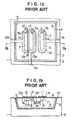
- a dielectric isolation substrate 1 includes a polycrystalline silicon support region 2, a silicon oxide film 3 acting as a dielectric film, and a single crystal silicon island region 4 acting as an n-type semiconductor matrix. Practically, the substrate 1 has a great number of island regions embedded in the support region 2.
- An n-type layer 5 of high impurity concentration intervenes between the island region 4 and the oxide film 3.
- a p-type emitter layer 6 and a p-type base layer 7, both in the form of an elongated strip, are formed by impurity diffusion in one major surface of the island region 4. The two elongated layers are in parallel with each other.
- n-type emitter layer 8 In the p-type base layer 7, is formed by impurity diffusion an n-type emitter layer 8 in a portion close to the p-type emitter layer 6.
- An undoped portion of the island region 4 stands for an n-type base layer 9, and a four-layer lateral thyristor is thus constituted by the p-type emitter layer 6, n-type base layer 9, p-type base layer 7 and n-type emitter layer 8.
- an oxide film 10 acting as a surface passivation film.
- Electrodes 11 to 13 for the anode, gate and cathode make ohmic contact to the p-type emitter layer 6, p-type base layer 7 and n-type emitter layer 8, respectively, through windows formed in the oxide film 10.
- the respective electrodes 11 to 13 have portions acting as field plates lla to 13a at areas dotted in Fig. la.
- the field plate lla extends beyond a pn-junction J1 formed between the p-type emitter layer 6 and the n-type base layer 9 to overlie the n-type base layer 9 through the oxide film 10.
- the field plates 12a and 13a extend beyond a pn-junction J 2 formed between the n-type base layer 9 and the p-type base layer 7 to overlie the n-type base layer 9 through the oxide film 10.
- the field plate lla surrounds the pn-junction J l
- the field plate 12a cooperates with the field plate 13a to substantially surround the pn-junction J 2 .
- the field plate 12a opposes the field plate 13a through a spacing which is large enough to prevent discharge across the spacing by a voltage applied between the two field plates.
- Formed on the oxide film 10 are wiring conductors llb to 13b which extend from the electrodes 11 to 13 so as to be connected to predetermined portions of an adjacent island region not shown.
- the electrodes 11 to 13 integral with the field plates lla to 13a and the wiring conductors llb to 13b are formed simultaneously through vapor deposition process.
- a depletion layer is created in the n-type base layer 9 and extended by the field plate lla.
- a voltage for backward biasing the pn-junction J 2 is applied, a depletion layer created in the n-type base layer 9 is extended by the field plates 12a and 13a. In proportion to the extension of the depletion layer, concentration of electric field within the depletion layer can be suppressed, evidencing effects which the field plate attains.
- the field concentration is liable to occur at ends or edges or corners of the pn-junctions J 1 and J 2 .
- Ends of the pn-junctions J 1 and J 2 are also rounded with corner radii r 1 and r 2 for improving the breakdown voltage.
- corner radii r 1 and r 2 of the pn-junctions J 1 and J 2 are centered at the same position as the corner radii R l to R 3 of the field plates lla to 13a, as shown in Fig. la.
- Linear portions of the field plates lla to 13a are designed to have a configuration which is in conformity with that of the ends of corner radii R 1 to R 3 . More particularly, letting widths of the linear portions of the field plates be W 1 , W 2 and W 3 , the corner radii R1, R 2 and R 3 are r l + W 1 , r 2 + W 2 and r2 + W 3 , respectively. This means that the field plate lla has a single extension width regardless of its position, i.e. at its linear portion and at its end to surround the pn-junction J 1 . This also holds - true for the field plates 12a and 13a which surround the pn-junction J 2 .
- the corner radii of the pn-junctions J 1 and J 2 in the depth dimension tend to be decreased. Difficulty of increasing the corner radius in the depth dimension as well as in the planar dimension makes it difficult to increase the breakdown voltage, even with the provision of the field plates lla to 13a.
- An object of this invention is therefore to provide a semiconductor device adapted to be incorporated in an integrated circuit, and capable of improving the breakdown voltage by providing a field plate.
- Another object of this invention is to provide a semiconductor device adapted to be incorporated in an integrated circuit, in which the device is provided with field plates and can improve the breakdown voltage without degrading various characteristics of the device.
- Still another object of this invention is to provide a semiconductor device adapted to be incorporated in a semiconductor integrated circuit, in which the device is provided with a field plate and can improve the breakdown voltage without increasing the size of the device.
- an elongated, doped semiconductor region in a lateral semiconductor element is surrounded by a field plate which has a larger width at its end than that at its linear portion.
- a depletion layer at the end can be extended to release concentration of electric field.
- a high breakdown voltage can be maintained in the linear portion of the field plate, a high breakdown voltage can be obtained without increasing a spacing between the opposing doped regions and without decreasing a spacing between opposing field plates.
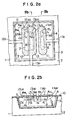
- FIG. 2a and 2b A semiconductor integrated circuit comprising a lateral thyristor according to an embodiment of the present invention is illustrated in Figs. 2a and 2b in which like elements as those in Figs. la and lb are designated by like reference numeals. To avoid prolixity of description, like elements will not be described hereinbelow.
- a p-type emitter layer 6 and a p-type base layer 7 are both in the form of an elongated strip and rounded at their ends with corner radii r 1 and r 2 .
- Electrodes 11 to 13 for anode, gate and cathode have portions acting as field plates lla, 12a and 13a, and these field plates are also rounded at their corners with radii R 1 , R 2 and R 3 .
- the corner radii r 1 to r 3 are not centered at the same position as the center of the corner radii R 1 to R 3 but centers of the former radii are displaced from those of the latter radii.
- the field plates lla, 12a and 13a respectively have, at their ends llaa, 12aa and 13aa, widths W 1a ' W 2a and W 3a which are respectively larger than widths W 1b , W 2b and W 3b at their linear portions llab, 12ab and 13ab.
- Edges of the depletion layers D 1 and D 2 created around the pn-junctions J 1 and J 2 under the respective reverse bias states in an n-type base layer 9 are superposedly shown at chained lines in Fig. 2b. It will be apparent that one of the junctions J 1 and J 2 is reverse-biased at one time.
- the depletion layer may be considered as a dielectric medium and an electric field is established therein. Electric fields immediately beneath the linear portions llab and 13ab exhibit parallel equi-potential surfaces and a high breakdown voltage can be maintained. As will be clear from Fig.
- the depletion layers D 1 and D 4 below the field plate ends llaa and 13aa is expanded Longer than those below the field plate linear portions llab and 13ab. Therefore, in the depletion layers immediately beneath the ends llaa and 13aa, field concentration can not take place and a high breakdown voltage can be maintained.
- a depletion layer immediately beneath the field plate 12a is not depicted. It should however be understood that since potentials at the gate electrode 12 and the cathode electrode 13 are substantially similar in comparison with the potential at the anode electrode 11, the depletion layer immediately beneath the field plate 12a generally has a configuration similar to that of the depletion layer D 2 immediately beneath the field plate 13. Accordingly, a depletion layer immediately beneath the end 12aa of the field plate 12a is also expanded and a high breakdown voltage can be maintained.
- the widths W 1a , W 2a and W 3a of the field plate ends llaa, 12aa and l3aa are simply required to be larger than the widths W lb' W 2b and W 3b of the field plate linear portions llab, 12ab and 13ab whereas there is no need of decreasing the spacing G1 between the linear portions, increasing the spacing G 2 between the p-type emitter layer 6 and the p-type base layer 7, or decreasing the length of an n-type emitter layer 8. Accordingly, it is possible to improve the breakdown voltage without impairing characteristics of the thyristor by simply changing the configuration of the field plate. Further, thanks to unnecessity of increasing the width of the p-type emitter layer 6, the packing density is not degreaded.
- the corner radius r 1 of the p-type emitter layer 6 was 15 um
- the width W lb of linear portion llab of the field plate lla was 20 ⁇ m
- the corner radius R 1 of end llaa of the field plate lla was 35 ⁇ m.
- the corner radius of the end of the p-type emitter layer 6 and the corner radius of the end of the field plate lla were centered at the same position but in the sample according to the invention, the displacement between the end corner radius center of the p-type emitter layer 6 and the end corner radius center of the field plate lla, that is, the distance between two centers was 20 ⁇ m.
- the breakdown voltage was about 350 V and with the sample of the present invention, the breakdown voltage was raised by 20 to 50 V.
- the raised amount of the breakdown voltage remained substantially unchanged when the displacement between the end corner radius center of the p-type emitter layer 6 and the end corner radius center of the field plate lla was changed within a range of 20 to 50 ⁇ m.
- the breakdown voltage could be improved or raised by modifying the configuration of the field plate end from the semicircular form into any convexly curved form such as an elliptical form or a hyperbolic form.
- Figs. 3a and 3b show a semiconductor integrated circuit comprising a lateral three-layer transistor.
- like elements as those in Figs. 2a and 2b are designated by like reference numerals.
- a p-type collector layer 21 and a p-type emitter layer 22, both in the form of an elongated strip, are formed by impurity diffusion in one major surface of an island region 4 which is an n-type semiconductor matrix. These layers are in parallel with each other. Ends of the two layers 21 and 22 are rounded.
- An undoped region 23 and an n-type high impurity concentration layer 5 through which the island region 4 adjoins an oxide film 3 constitute a base layer.
- a collector electrode 24 and an emitter electrode 25 make ohmic contact with the p-type collector region 21 and the p-type emitter region 22, respectively, through windows formed in a silicon oxide film 10 serving as a surface passivation film on the island region.
- the collector electrode 24 and the emitter electrode 25 have portions acting as field plates 24a and 25a which surround pn-junctions J 1 and J 2 .
- Wiring conductors 24b and 25b are integral with the field plates 24a and 25a corresponding to dotted areas in Fig. 3a.
- a base electrode 26 makes ohmic contact to the high impurity concentration layer 5.
- opposite ends 24aa of the field plate 24a contiguous to opposite ends of the p-type collector layer 21 are designed to have a width which is larger than that of linear portions 24ab. Since the emitter junction J 2 does not require so high a breakdown voltage as the collector junction J 1 , the field plate 25a has the same width at its ends 25aa and at its linear portions 25ab.
- a spacing G 4 between the collector layer 21 and the emitter layer 22 needs not be increased so that current amplification factor h FE of the transistor will not be reduced. Also, the collector layer 21 needs not be increased in area, thereby preventing decrease in the integration density.
- the field plate having a larger width at its ends than at its linear portions can reduce the concentration of electric field at the ends of the doped region, thereby attaining compatibility with the reduction in width and thickness of those diffusion regions.
- the p-type doped regions are formed in the n-type semiconductor matrix for illustration purpose only but obviously, the present invention may be applicable to a semiconductor devices wherein n-type doped regions are formed in a p-type semiconductor matrix.
- the isolated island substrate as described in terms of a dielectric isolation type may be of a pn-junction isolation type or an air separation type.
- an n-type emitter layer may be disposed remote from a p-type emitter layer and a gate electrode may be interposed between an anode electrode and a cathode electrode.
- the corner radius at the end of the field plate be a sum of the linear portion width and the corner radius of the diffusion region to which the electrode integral with the field plate makes low resistance contact.
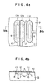
- Figs. 4a and 4b show a lateral gate turn-off thyristor formed in one island region of a semiconductor integrated circuit, wherein like elements as those in Figs. 2a and 2b are designated by like reference numerals.
- an n-type emitter layer 8 formed in a p-type base layer 7 is remote from a p-type emitter layer 6, and a gate electrode 12 in ohmic contact with the p-type base layer 7 is interposed between an anode electrode 11 in ohmic contact with the p-type emitter layer 6 and a cathode electrode 13 in ohmic contact with the n-type emitter layer 8.
- the gate electrode 12 has a portion serving as a field plate 12a and the cathode electrode 13 has a portion serving as a field plate 13a.
- the field plates 12a and 13a surround the substantial entirety of a pn-junction J 2 .
- Turning-off of the thyristor is achieved by drawing holes flowing from the p-type emitter layer 6 to the n-type emitter layer 8 (in the on-state) out of the gate electrode 12. According to this structure, holes can readily be drawn out since the gate electrode 12 is disposed close to and opposing to the anode electrode 11.
- the breakdown voltage of the thyristor can be improved without changing a spacing G 1 between the field plates lla and 13a and a spacing G 2 between the p-type emitter layer 6 and the p-type base layer 7.
- Fig. 5 shows a thyristor modified from the thyristor shown in Figs. 2a and 2b.
- like elements as those in Figs. 2a and 2b are designated by like reference numerals.
- This modification is different from the embodiment of Figs. 2a and 2b in that corner radii at ends of field plates are dimensioned differently.
- a corner radius R1 at an end llaa of a field plate lla integral with an anode electrode 11 in ohmic contact with a p-type emitter layer 6 is smaller than a sum of a corner radius r 1 of the p-type emitter layer 6 and a width W lb of a linear portion llab of the field plate lla.
- a corner radius R 2 at an end l3aa of a field plate 13a integral with a cathode electrode 13 in ohmic contact with an n-type emitter layer 8 is larger than a sum of a corner radius r 2 and a width W 3b of a linear portion 13ab of the field plate 13a. Namely, R 1 ⁇ r l + W 1b and R 2 > r 2 + W 3b stand.
- This construction is based on the fact that a high breakdown voltage can be obtained if the linear portion llab of the field plate lla opposes the linear portion l3ab of the field plate 13a with a spacing G I therebetween, and the end width W la and the linear portion width W lb of the field plate lla establish a relation W 1a > W 1b' and/or the end width W 3a and the linear portion width W 3b of the field plate 13a establish a relation W 3a > W 3b .
- the construction as shown in Fig. 5 is effective when a pn-junction J 2 is required to have a particularly high breakdown voltage which is higher than a breakdown voltage required for a pn-junction J 1 .
- the corner radius R 1 may be u p to r 1 + W lb .
- the condition of r 2 + W 3b ⁇ R 2 or r 2 + W 3b > R 2 can be selected dependent on required characteristics. This is because the width of the p-type emitter layer 6 is too narrow to have tolerance whereas the p-type base layer 7 includes the n-type emitter layer 8 and has a width larger than that of the p-type emitter layer 6, thus having tolerance.
- a narrow portion of a doped region is responsive to the breakdown voltage of the associated pn-junction and that extending a field plate at such a narrow portion longer than at a wider portion will improve the breakdown voltage.
Landscapes
- Electrodes Of Semiconductors (AREA)
- Thyristors (AREA)
- Bipolar Transistors (AREA)
Applications Claiming Priority (2)
| Application Number | Priority Date | Filing Date | Title |
|---|---|---|---|
| JP57147779A JPS5939066A (ja) | 1982-08-27 | 1982-08-27 | 半導体集積回路 |
| JP147779/82 | 1982-08-27 |
Publications (3)
| Publication Number | Publication Date |
|---|---|
| EP0104454A2 true EP0104454A2 (fr) | 1984-04-04 |
| EP0104454A3 EP0104454A3 (en) | 1985-09-25 |
| EP0104454B1 EP0104454B1 (fr) | 1989-03-01 |
Family
ID=15437992
Family Applications (1)
| Application Number | Title | Priority Date | Filing Date |
|---|---|---|---|
| EP83108420A Expired EP0104454B1 (fr) | 1982-08-27 | 1983-08-26 | Dispositif semi-conducteur ayant un écran |
Country Status (5)
| Country | Link |
|---|---|
| US (1) | US4654691A (fr) |
| EP (1) | EP0104454B1 (fr) |
| JP (1) | JPS5939066A (fr) |
| CA (1) | CA1190663A (fr) |
| DE (1) | DE3379299D1 (fr) |
Cited By (4)
| Publication number | Priority date | Publication date | Assignee | Title |
|---|---|---|---|---|
| FR2594596A1 (fr) * | 1986-02-18 | 1987-08-21 | Thomson Csf | Structure semiconductrice associant un ou plusieurs transistors de puissance et leur logique de commande et de protection |
| DE3806164A1 (de) * | 1987-02-26 | 1988-09-08 | Toshiba Kawasaki Kk | Halbleiterbauelement mit hoher durchbruchspannung |
| EP0181002A3 (en) * | 1984-11-09 | 1988-09-21 | Hitachi, Ltd. | Semiconductor device having high breakdown voltage |
| US5241210A (en) * | 1987-02-26 | 1993-08-31 | Kabushiki Kaisha Toshiba | High breakdown voltage semiconductor device |
Families Citing this family (6)
| Publication number | Priority date | Publication date | Assignee | Title |
|---|---|---|---|---|
| JP2513617B2 (ja) * | 1986-01-24 | 1996-07-03 | 株式会社東芝 | 正規化回路 |
| US4786958A (en) * | 1986-11-17 | 1988-11-22 | General Motors Corporation | Lateral dual gate thyristor and method of fabricating same |
| US4861731A (en) * | 1988-02-02 | 1989-08-29 | General Motors Corporation | Method of fabricating a lateral dual gate thyristor |
| JP2507557B2 (ja) * | 1988-09-29 | 1996-06-12 | 三菱電機株式会社 | 半導体装置の製造方法 |
| US5107312A (en) * | 1989-09-11 | 1992-04-21 | Harris Corporation | Method of isolating a top gate of a MESFET and the resulting device |
| JP2903749B2 (ja) * | 1991-03-29 | 1999-06-14 | 富士電機株式会社 | 伝導度変調型misfetを備えた半導体装置 |
Family Cites Families (7)
| Publication number | Priority date | Publication date | Assignee | Title |
|---|---|---|---|---|
| GB1140822A (en) * | 1967-01-26 | 1969-01-22 | Westinghouse Brake & Signal | Semi-conductor elements |
| JPS54122983A (en) * | 1978-03-17 | 1979-09-22 | Hitachi Ltd | Semiconductor integrated circuit |
| JPS584829B2 (ja) * | 1978-03-31 | 1983-01-27 | 日本電信電話株式会社 | 半導体集積回路 |
| JPS55133553A (en) * | 1979-04-03 | 1980-10-17 | Hitachi Ltd | Semiconductor integrated device |
| JPS5753944A (en) * | 1980-09-17 | 1982-03-31 | Hitachi Ltd | Semiconductor integrated circuit |
| US4412242A (en) * | 1980-11-17 | 1983-10-25 | International Rectifier Corporation | Planar structure for high voltage semiconductor devices with gaps in glassy layer over high field regions |
| JPH108771A (ja) * | 1996-06-21 | 1998-01-13 | Mitsubishi Steel Mfg Co Ltd | 建造物用制振装置 |
-
1982
- 1982-08-27 JP JP57147779A patent/JPS5939066A/ja active Granted
-
1983
- 1983-08-23 CA CA000435178A patent/CA1190663A/fr not_active Expired
- 1983-08-26 EP EP83108420A patent/EP0104454B1/fr not_active Expired
- 1983-08-26 DE DE8383108420T patent/DE3379299D1/de not_active Expired
-
1986
- 1986-01-07 US US06/816,979 patent/US4654691A/en not_active Expired - Fee Related
Cited By (5)
| Publication number | Priority date | Publication date | Assignee | Title |
|---|---|---|---|---|
| EP0181002A3 (en) * | 1984-11-09 | 1988-09-21 | Hitachi, Ltd. | Semiconductor device having high breakdown voltage |
| FR2594596A1 (fr) * | 1986-02-18 | 1987-08-21 | Thomson Csf | Structure semiconductrice associant un ou plusieurs transistors de puissance et leur logique de commande et de protection |
| EP0236200A1 (fr) * | 1986-02-18 | 1987-09-09 | Thomson-Csf | Structure semiconductrice associant un ou plusieurs transistors de puissance, et leur logique de commande et de protection |
| DE3806164A1 (de) * | 1987-02-26 | 1988-09-08 | Toshiba Kawasaki Kk | Halbleiterbauelement mit hoher durchbruchspannung |
| US5241210A (en) * | 1987-02-26 | 1993-08-31 | Kabushiki Kaisha Toshiba | High breakdown voltage semiconductor device |
Also Published As
| Publication number | Publication date |
|---|---|
| US4654691A (en) | 1987-03-31 |
| DE3379299D1 (en) | 1989-04-06 |
| JPS5939066A (ja) | 1984-03-03 |
| EP0104454B1 (fr) | 1989-03-01 |
| JPH0139661B2 (fr) | 1989-08-22 |
| EP0104454A3 (en) | 1985-09-25 |
| CA1190663A (fr) | 1985-07-16 |
Similar Documents
| Publication | Publication Date | Title |
|---|---|---|
| US5324971A (en) | Power semiconductor device having over voltage protection | |
| US5315139A (en) | Power semiconductor integrated circuit device without concentration of electric field | |
| US4750028A (en) | Semiconductor device having floating semiconductor zones | |
| US5869882A (en) | Zener diode structure with high reverse breakdown voltage | |
| US6310365B1 (en) | Surface voltage sustaining structure for semiconductor devices having floating voltage terminal | |
| US5352915A (en) | Semiconductor component having two integrated insulated gate field effect devices | |
| EP0104454B1 (fr) | Dispositif semi-conducteur ayant un écran | |
| US5327006A (en) | Thin, dielectrically isolated island resident transistor structure having low collector resistance | |
| EP0181002A2 (fr) | Dispositif semi-conducteur à haute tension de claquage | |
| US6765262B2 (en) | Vertical high-voltage semiconductor component | |
| US5391908A (en) | Lateral insulated gate field effect semiconductor | |
| EP0660416A1 (fr) | Dispositif semi-conducteur avec surface de bord réduite et haute tension de claquage | |
| US3631312A (en) | High-voltage mos transistor method and apparatus | |
| JP2937185B2 (ja) | 高破壊耐量mos型半導体装置 | |
| US4361846A (en) | Lateral type semiconductor devices with enlarged, large radii collector contact regions for high reverse voltage | |
| EP0557126A1 (fr) | Dispositif semi-conducteur de puissance | |
| JP3522433B2 (ja) | 薄膜半導体装置 | |
| EP4113623A1 (fr) | Dispositif de transistor | |
| US4520382A (en) | Semiconductor integrated circuit with inversion preventing electrode | |
| US6831338B1 (en) | Power component bearing interconnections | |
| US5488241A (en) | Integrated device combining a bipolar transistor and a field effect transistor | |
| EP0107252B1 (fr) | Dispositif semi-conducteur | |
| EP0673072A2 (fr) | Dispositifs semi-conducteurs bipolaires | |
| US5324978A (en) | Semiconductor device having an improved breakdown voltage-raising structure | |
| US10847610B2 (en) | Semiconductor device |
Legal Events
| Date | Code | Title | Description |
|---|---|---|---|
| PUAI | Public reference made under article 153(3) epc to a published international application that has entered the european phase |
Free format text: ORIGINAL CODE: 0009012 |
|
| AK | Designated contracting states |
Designated state(s): DE FR GB |
|
| PUAL | Search report despatched |
Free format text: ORIGINAL CODE: 0009013 |
|
| AK | Designated contracting states |
Designated state(s): DE FR GB |
|
| 17P | Request for examination filed |
Effective date: 19850927 |
|
| 17Q | First examination report despatched |
Effective date: 19861212 |
|
| GRAA | (expected) grant |
Free format text: ORIGINAL CODE: 0009210 |
|
| AK | Designated contracting states |
Kind code of ref document: B1 Designated state(s): DE FR GB |
|
| REF | Corresponds to: |
Ref document number: 3379299 Country of ref document: DE Date of ref document: 19890406 |
|
| ET | Fr: translation filed | ||
| PLBE | No opposition filed within time limit |
Free format text: ORIGINAL CODE: 0009261 |
|
| STAA | Information on the status of an ep patent application or granted ep patent |
Free format text: STATUS: NO OPPOSITION FILED WITHIN TIME LIMIT |
|
| 26N | No opposition filed | ||
| PGFP | Annual fee paid to national office [announced via postgrant information from national office to epo] |
Ref country code: FR Payment date: 19920630 Year of fee payment: 10 |
|
| PGFP | Annual fee paid to national office [announced via postgrant information from national office to epo] |
Ref country code: GB Payment date: 19920814 Year of fee payment: 10 |
|
| PGFP | Annual fee paid to national office [announced via postgrant information from national office to epo] |
Ref country code: DE Payment date: 19921026 Year of fee payment: 10 |
|
| PG25 | Lapsed in a contracting state [announced via postgrant information from national office to epo] |
Ref country code: GB Effective date: 19930826 |
|
| GBPC | Gb: european patent ceased through non-payment of renewal fee |
Effective date: 19930826 |
|
| PG25 | Lapsed in a contracting state [announced via postgrant information from national office to epo] |
Ref country code: FR Effective date: 19940429 |
|
| PG25 | Lapsed in a contracting state [announced via postgrant information from national office to epo] |
Ref country code: DE Effective date: 19940503 |
|
| REG | Reference to a national code |
Ref country code: FR Ref legal event code: ST |
|
| PGFP | Annual fee paid to national office [announced via postgrant information from national office to epo] |
Ref country code: LU Payment date: 19960701 Year of fee payment: 7 |