EP0104754B1 - Dispositif métal-isolant semi-conducteur à région de source liée à une tension de référence - Google Patents
Dispositif métal-isolant semi-conducteur à région de source liée à une tension de référence Download PDFInfo
- Publication number
- EP0104754B1 EP0104754B1 EP83304814A EP83304814A EP0104754B1 EP 0104754 B1 EP0104754 B1 EP 0104754B1 EP 83304814 A EP83304814 A EP 83304814A EP 83304814 A EP83304814 A EP 83304814A EP 0104754 B1 EP0104754 B1 EP 0104754B1
- Authority
- EP
- European Patent Office
- Prior art keywords
- source region
- semiconductor device
- source
- substrate
- region
- Prior art date
- Legal status (The legal status is an assumption and is not a legal conclusion. Google has not performed a legal analysis and makes no representation as to the accuracy of the status listed.)
- Expired
Links
Images


Classifications
-
- H—ELECTRICITY
- H10—SEMICONDUCTOR DEVICES; ELECTRIC SOLID-STATE DEVICES NOT OTHERWISE PROVIDED FOR
- H10D—INORGANIC ELECTRIC SEMICONDUCTOR DEVICES
- H10D62/00—Semiconductor bodies, or regions thereof, of devices having potential barriers
- H10D62/10—Shapes, relative sizes or dispositions of the regions of the semiconductor bodies; Shapes of the semiconductor bodies
- H10D62/13—Semiconductor regions connected to electrodes carrying current to be rectified, amplified or switched, e.g. source or drain regions
- H10D62/149—Source or drain regions of field-effect devices
- H10D62/151—Source or drain regions of field-effect devices of IGFETs
-
- H—ELECTRICITY
- H10—SEMICONDUCTOR DEVICES; ELECTRIC SOLID-STATE DEVICES NOT OTHERWISE PROVIDED FOR
- H10D—INORGANIC ELECTRIC SEMICONDUCTOR DEVICES
- H10D30/00—Field-effect transistors [FET]
- H10D30/60—Insulated-gate field-effect transistors [IGFET]
-
- H—ELECTRICITY
- H10—SEMICONDUCTOR DEVICES; ELECTRIC SOLID-STATE DEVICES NOT OTHERWISE PROVIDED FOR
- H10D—INORGANIC ELECTRIC SEMICONDUCTOR DEVICES
- H10D64/00—Electrodes of devices having potential barriers
- H10D64/20—Electrodes characterised by their shapes, relative sizes or dispositions
- H10D64/23—Electrodes carrying the current to be rectified, amplified, oscillated or switched, e.g. sources, drains, anodes or cathodes
- H10D64/251—Source or drain electrodes for field-effect devices
Definitions
- the present invention relates to a semiconductor device and more particularly to a semiconductor device comprising metal insulator semiconductor (MIS)field effecttransistors (FET) in which a wiring line for a reference voltage supply is not needed.
- MIS metal insulator semiconductor
- FET field effecttransistors
- a semiconductor device such as a logic integrated circuit or a microprocessor device has a large number of wiring lines connecting various elements.
- Such wiring lines include voltage supply lines, various signal lines, input lines, output lines, and ground lines. These wiring lines occupy a relatively large area of the semiconductor device and generally determine the scale of integration of an integrated circuit. Ground lines in particular, occupy a considerable area and complicate the pattern layout of the integrated circuit.
- each MIS FET formed in the semiconductor substrate is usually connected to a reference voltage wiring line through a contact window that opens onto the surface of the substrate.
- the semiconductor substrate is also supplied with a reference voltage using a back electrode attached to the rear face of the integrated circuit chip.
- DE-A-2825433 discloses a semiconductor device including MIS FETS with the sources of the MIS FET's connected to a reference voltage source through a wiring line extending through a contact window and over the surface of the device.
- the substrate at the same potential as the source region and, to achievethiswithoutthe need for a back electrode attached to the rear face of the integrated circuit chip an alloy region is formed beneath the source electrode to connect the source region directly to the substrate. In this way the potential on a wiring line leading through a contact region and into contact with the source electrode is also connected to the substrate without a back electrode.
- a semiconductor device comprising at least one metal-insulator-semiconductor field effect transistor formed on a semiconductor substrate, and field effect transistor comprising a drain region and a source region of one conductivity type formed in a region of the semiconductor substrate of another conductivity type, also includes means forming a direct electrical connection between the source region and the semiconductor substrate with said means provid-' ing the sole electrical connection between said source region and a wiring line provided on the back surface of the substrate.
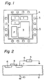
- Figure 1 is a schematic plan view of a prior art integrated circuit semiconductor device.
- reference numeral 1 is a D/A (digital-to-analog) converter with 6-bit precision
- 2 is an address recorder
- 3 is a D/A counter with 13-bit precision
- 4 is a reference voltage (ground) wiring line
- 5 is a pad.
- the integrated circuit of Fig. 1 comprises MIS FET's.
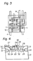
- FIG. 2 is a schematic cross-sectional view of an MIS FET in the integrated circuit of Fig. 1.
- reference numeral 6 is a drain region
- 7 is a source region
- 8 is a gate electrode
- 9 is a semiconductor substrate
- 10 is a ground line.
- the semiconductor substrate 9 is of one conductivity type
- the drain and source regions 6 and 7 are of the opposite conductivity type. Since a pn junction is formed between the source region 7 and the semiconductor substrate 9, the source region 7 is not electrically connected to the semiconductor substrate 9.
- the source region 7 is connected to the reference voltage wiring line 4 at the surface of the substrate 9, the reference voltage wiring line 4 is connected to one pad 5, and the pad 5 is connected externally to the ground.
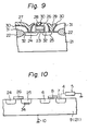
- Figure 3 is the wiring pattern layout of a main portion of the semiconductor device of Fig. 1.
- reference numeral 11 is an electrode contact window
- 12 is a diffusion layerfor drain and source regions
- 13 is a polycrystalline silicon layer forming a gate electrode and a wiring line for it
- 14 and 4 are aluminum (Al) wiring lines.
- the wiring lines, especially the ground wiring lines, occupy a considerably large area. These largely determine the scale of integration of the integrated circuit and complicate the pattern layout of the integrated circuit.
- FIG. 4 is a cross-sectional view of a MIS FET included in a semiconductor device according to the invention.
- reference numeral 21 is a p-type silicon substrate
- 22 is a field oxide film
- 23 is a gate oxide film
- 24 is a drain region
- 25 is a source region
- 26 is a gate electrode
- 27 is an AI drain electrode wiring line
- 28 is a gate wiring line
- 29 is a source electrode
- 30 is a polycrystalline silicon film
- 31 is an insulator film
- 32 is a thin oxide film.
- the source electrode 29 is not connected to any wiring line to which a reference voltage is applied. Instead, the source region is directly connected to the substrate 21 as described below.
- the source electrode 29 is formed so as to contact the source region 25 without a polycrystalline silicon layer under the source electrode 29.
- the aluminum in the source electrode 29 is impregnated into the source region 25. Some of this aluminum is further impregnated into the substrate 21 through the source region 25. The source region 25 and the substrate 21 are therefore electrically connected through the impregnated aluminum.
- the potential of the source region 25 thus becomes equal to that of the substrate 21. Since the substrate 21 is connected to a ground line at the back surface (opposite surface from that on which active elements are formed), the potential- of the substrate 21 is equal to the ground level, which in turn makes the potential of the source region 25 equal to the ground level.
- Figure 5 is a schematic cross-sectional view of the semiconductor device of Fig. 4.
- portions corresponding to those in Fig. 4 are designated by the same reference numerals.
- Reference numeral 34 is the impregnated aluminum.
- no wiring line for connecting the source region 25 to the reference voltage is formed on the surface of the substrate 21.
- Figure 6 is a schematic plan view of the semiconductor device according to the present invention, in which all the source regions having the reference voltage are connected directly to the substrate as described above. In such a semiconductor device, no wiring lines 4 for the reference voltage are necessary. Thus, the surface area devoted to circuiting in the semiconductor device of Fig. 6 is decreased by an area corresponding to the reference voltage wiring lines 4, as compared with the surface area of the prior, art semiconductor device of Fig. 1. An outline of the prior art semiconductor device is shown with a broken line in Fig. 6 for the purpose of comparison.
- Figure 7 is a pattern layout of a main portion of the semiconductor device of Fig. 6.
- Fig. 6 corresponding portions are given the same reference numerals as in Fig. 3.
- the pattern layout of the semiconductor device according to the present invention is simplified by eliminating the reference voltage wiring line led out from the source electrode.
- FIG. 8 is a cross-sectional view of a semiconductor device in accordance with a second embodiment of the present invention.
- corresponding portions are given the same reference numerals as in Fig. 4.
- the diffusion layer for the drain region 24 is formed in such a manner that the depth of the layer at the portion below the contact window for the drain electrode 27 is greater than the other portions.
- the aluminum that impregnates the drain region 24 from drain electrode 27 does not reach the silicon substrate 21.
- the depth of the diffusion layer for the source region 25-- is not so great that the impregnated aluminum from the source electrode 29 reaches the silicon substrate 21.
- the source region 25 is connected directly to the substrate 21 by the impregnated aluminum, but the drain region 24 is electrically isolated from the substrate 21 by the pn junction formed therebetween.
- Figure 9 is a cross-sectional view of a semiconductor device in accordance with a third embodiment of the present invention.
- corresponding portions are given the same reference numerals as in Fig. 4.
- the construction of the semiconductor device of Fig. 9 is essentially identical to that of the semiconductor device of Fig. 4, except that the contact window for the source region 25 is formed at the boundary portion of the source region 25 so that the source electrode 29 has contact with both the source region 25 and the silicon substrate 21 through a polycrystalline silicon layer 30. Accordingly, in the semiconductor device of Fig. 9, the source region 25 and the silicon substrate 21 are electrically connected through the source electrode 29.
- the area necessary for forming an integrated circuit can be decreased so that the scale of integration of the integrated circuit can be increased.
- the present invention is preferably applied to a small supply current circuit, such as a complementary metal- oxide semiconductor (CMOS) circuit.
- CMOS complementary metal- oxide semiconductor
- a semiconductor device comprises both small current MIS transistors and rather large current MIS transistor, it is preferable that the source regions of the small current MIS transistors be connected directly to the substrate, and the source regions of the large current MIS transistors be connected to the reference voltage wiring lines through the contact windows.
- Figure 10 is a schematic cross-sectional view of such a semiconductor device.
- corresponding portions are given with the same reference numerals as in Figs. 2 and 5.
Landscapes
- Metal-Oxide And Bipolar Metal-Oxide Semiconductor Integrated Circuits (AREA)
- Semiconductor Integrated Circuits (AREA)
Claims (5)
Applications Claiming Priority (2)
| Application Number | Priority Date | Filing Date | Title |
|---|---|---|---|
| JP167920/82 | 1982-09-27 | ||
| JP57167920A JPS5957477A (ja) | 1982-09-27 | 1982-09-27 | 半導体装置 |
Publications (2)
| Publication Number | Publication Date |
|---|---|
| EP0104754A1 EP0104754A1 (fr) | 1984-04-04 |
| EP0104754B1 true EP0104754B1 (fr) | 1986-08-13 |
Family
ID=15858501
Family Applications (1)
| Application Number | Title | Priority Date | Filing Date |
|---|---|---|---|
| EP83304814A Expired EP0104754B1 (fr) | 1982-09-27 | 1983-08-19 | Dispositif métal-isolant semi-conducteur à région de source liée à une tension de référence |
Country Status (3)
| Country | Link |
|---|---|
| EP (1) | EP0104754B1 (fr) |
| JP (1) | JPS5957477A (fr) |
| DE (1) | DE3365293D1 (fr) |
Families Citing this family (5)
| Publication number | Priority date | Publication date | Assignee | Title |
|---|---|---|---|---|
| FR2570880A1 (fr) * | 1984-09-27 | 1986-03-28 | Rca Corp | Procede de fabrication d'un transistor a effet de champ a grille isolee et transistor ainsi obtenu |
| US5234853A (en) * | 1990-03-05 | 1993-08-10 | Fujitsu Limited | Method of producing a high voltage MOS transistor |
| US5140392A (en) * | 1990-03-05 | 1992-08-18 | Fujitsu Limited | High voltage mos transistor and production method thereof, and semiconductor device having high voltage mos transistor and production method thereof |
| US5895766A (en) * | 1995-09-20 | 1999-04-20 | Micron Technology, Inc. | Method of forming a field effect transistor |
| JP2000349096A (ja) * | 1999-06-01 | 2000-12-15 | Matsushita Electric Ind Co Ltd | 化合物電界効果トランジスタおよびその製造方法 |
Family Cites Families (5)
| Publication number | Priority date | Publication date | Assignee | Title |
|---|---|---|---|---|
| US3649843A (en) * | 1969-06-26 | 1972-03-14 | Texas Instruments Inc | Mos bipolar push-pull output buffer |
| JPS49105490A (fr) * | 1973-02-07 | 1974-10-05 | ||
| JPS543480A (en) * | 1977-06-09 | 1979-01-11 | Fujitsu Ltd | Manufacture of semiconductor device |
| NL7904200A (nl) * | 1979-05-29 | 1980-12-02 | Philips Nv | Lagenveldeffecttransistor. |
| JPS56134757A (en) * | 1980-03-26 | 1981-10-21 | Nec Corp | Complementary type mos semiconductor device and its manufacture |
-
1982
- 1982-09-27 JP JP57167920A patent/JPS5957477A/ja active Pending
-
1983
- 1983-08-19 EP EP83304814A patent/EP0104754B1/fr not_active Expired
- 1983-08-19 DE DE8383304814T patent/DE3365293D1/de not_active Expired
Also Published As
| Publication number | Publication date |
|---|---|
| JPS5957477A (ja) | 1984-04-03 |
| DE3365293D1 (en) | 1986-09-18 |
| EP0104754A1 (fr) | 1984-04-04 |
Similar Documents
| Publication | Publication Date | Title |
|---|---|---|
| EP0154998B1 (fr) | Structure de conducteurs d'alimentation dans un circuit intégré semi-conducteur | |
| US4926243A (en) | High voltage MOS field effect semiconductor device | |
| JP3017809B2 (ja) | アナログ・デジタル混載半導体集積回路装置 | |
| JPH0558583B2 (fr) | ||
| US4764798A (en) | Master slice IC having n and p channel transistors | |
| US4691217A (en) | Semiconductor integrated circuit device | |
| GB2028585A (en) | On board integrated circuit chip signal source abstract of the disclosure | |
| KR100302529B1 (ko) | 박막반도체집적회로 | |
| HK1002542B (en) | Integrated circuit power supply contact | |
| HK1002542A1 (en) | Integrated circuit power supply contact | |
| JPS60171771A (ja) | 絶縁ゲ−ト半導体装置 | |
| US4251829A (en) | Insulated gate field-effect transistor | |
| EP0104754A1 (fr) | Dispositif métal-isolant semi-conducteur à région de source liée à une tension de référence | |
| JP2602974B2 (ja) | Cmos半導体集積回路装置 | |
| EP0708486B1 (fr) | Transistor semi-conducteur à effet de champ à région étendue en contact avec le substrat | |
| US5814860A (en) | Semiconductor IC device having first and second pads on surface of semiconductor chip | |
| JP2598446B2 (ja) | Mis−fet | |
| EP0083699A2 (fr) | Circuit de protection pour dispositifs semi-conducteurs | |
| JP3271435B2 (ja) | 半導体集積回路装置 | |
| GB2179494A (en) | Protection structure | |
| JP3217552B2 (ja) | 横型高耐圧半導体素子 | |
| JPH0846145A (ja) | 半導体回路装置 | |
| JPS584820B2 (ja) | 半導体装置 | |
| JPH0750392A (ja) | 半導体集積回路装置 | |
| US3612961A (en) | Semiconductor integrated circuit device |
Legal Events
| Date | Code | Title | Description |
|---|---|---|---|
| PUAI | Public reference made under article 153(3) epc to a published international application that has entered the european phase |
Free format text: ORIGINAL CODE: 0009012 |
|
| AK | Designated contracting states |
Designated state(s): DE FR GB |
|
| 17P | Request for examination filed |
Effective date: 19840822 |
|
| GRAA | (expected) grant |
Free format text: ORIGINAL CODE: 0009210 |
|
| AK | Designated contracting states |
Kind code of ref document: B1 Designated state(s): DE FR GB |
|
| ET | Fr: translation filed | ||
| REF | Corresponds to: |
Ref document number: 3365293 Country of ref document: DE Date of ref document: 19860918 |
|
| PLBE | No opposition filed within time limit |
Free format text: ORIGINAL CODE: 0009261 |
|
| STAA | Information on the status of an ep patent application or granted ep patent |
Free format text: STATUS: NO OPPOSITION FILED WITHIN TIME LIMIT |
|
| 26N | No opposition filed | ||
| PGFP | Annual fee paid to national office [announced via postgrant information from national office to epo] |
Ref country code: GB Payment date: 19900807 Year of fee payment: 8 |
|
| PGFP | Annual fee paid to national office [announced via postgrant information from national office to epo] |
Ref country code: FR Payment date: 19900830 Year of fee payment: 8 |
|
| PGFP | Annual fee paid to national office [announced via postgrant information from national office to epo] |
Ref country code: DE Payment date: 19901024 Year of fee payment: 8 |
|
| PG25 | Lapsed in a contracting state [announced via postgrant information from national office to epo] |
Ref country code: GB Effective date: 19910819 |
|
| GBPC | Gb: european patent ceased through non-payment of renewal fee | ||
| PG25 | Lapsed in a contracting state [announced via postgrant information from national office to epo] |
Ref country code: FR Effective date: 19920430 |
|
| PG25 | Lapsed in a contracting state [announced via postgrant information from national office to epo] |
Ref country code: DE Effective date: 19920501 |
|
| REG | Reference to a national code |
Ref country code: FR Ref legal event code: ST |