EP0104916A2 - Dépôt d'un film sur un substrat par évaporation à l'aide d'un faisceau d'électrons - Google Patents
Dépôt d'un film sur un substrat par évaporation à l'aide d'un faisceau d'électrons Download PDFInfo
- Publication number
- EP0104916A2 EP0104916A2 EP83305705A EP83305705A EP0104916A2 EP 0104916 A2 EP0104916 A2 EP 0104916A2 EP 83305705 A EP83305705 A EP 83305705A EP 83305705 A EP83305705 A EP 83305705A EP 0104916 A2 EP0104916 A2 EP 0104916A2
- Authority
- EP
- European Patent Office
- Prior art keywords
- process according
- substrate
- film
- supply
- gas
- Prior art date
- Legal status (The legal status is an assumption and is not a legal conclusion. Google has not performed a legal analysis and makes no representation as to the accuracy of the status listed.)
- Granted
Links
Images
Classifications
-
- H—ELECTRICITY
- H10—SEMICONDUCTOR DEVICES; ELECTRIC SOLID-STATE DEVICES NOT OTHERWISE PROVIDED FOR
- H10P—GENERIC PROCESSES OR APPARATUS FOR THE MANUFACTURE OR TREATMENT OF DEVICES COVERED BY CLASS H10
- H10P14/00—Formation of materials, e.g. in the shape of layers or pillars
- H10P14/20—Formation of materials, e.g. in the shape of layers or pillars of semiconductor materials
- H10P14/34—Deposited materials, e.g. layers
- H10P14/3402—Deposited materials, e.g. layers characterised by the chemical composition
- H10P14/3404—Deposited materials, e.g. layers characterised by the chemical composition being Group IVA materials
- H10P14/3411—Silicon, silicon germanium or germanium
-
- C—CHEMISTRY; METALLURGY
- C23—COATING METALLIC MATERIAL; COATING MATERIAL WITH METALLIC MATERIAL; CHEMICAL SURFACE TREATMENT; DIFFUSION TREATMENT OF METALLIC MATERIAL; COATING BY VACUUM EVAPORATION, BY SPUTTERING, BY ION IMPLANTATION OR BY CHEMICAL VAPOUR DEPOSITION, IN GENERAL; INHIBITING CORROSION OF METALLIC MATERIAL OR INCRUSTATION IN GENERAL
- C23C—COATING METALLIC MATERIAL; COATING MATERIAL WITH METALLIC MATERIAL; SURFACE TREATMENT OF METALLIC MATERIAL BY DIFFUSION INTO THE SURFACE, BY CHEMICAL CONVERSION OR SUBSTITUTION; COATING BY VACUUM EVAPORATION, BY SPUTTERING, BY ION IMPLANTATION OR BY CHEMICAL VAPOUR DEPOSITION, IN GENERAL
- C23C14/00—Coating by vacuum evaporation, by sputtering or by ion implantation of the coating forming material
- C23C14/0021—Reactive sputtering or evaporation
-
- C—CHEMISTRY; METALLURGY
- C23—COATING METALLIC MATERIAL; COATING MATERIAL WITH METALLIC MATERIAL; CHEMICAL SURFACE TREATMENT; DIFFUSION TREATMENT OF METALLIC MATERIAL; COATING BY VACUUM EVAPORATION, BY SPUTTERING, BY ION IMPLANTATION OR BY CHEMICAL VAPOUR DEPOSITION, IN GENERAL; INHIBITING CORROSION OF METALLIC MATERIAL OR INCRUSTATION IN GENERAL
- C23C—COATING METALLIC MATERIAL; COATING MATERIAL WITH METALLIC MATERIAL; SURFACE TREATMENT OF METALLIC MATERIAL BY DIFFUSION INTO THE SURFACE, BY CHEMICAL CONVERSION OR SUBSTITUTION; COATING BY VACUUM EVAPORATION, BY SPUTTERING, BY ION IMPLANTATION OR BY CHEMICAL VAPOUR DEPOSITION, IN GENERAL
- C23C14/00—Coating by vacuum evaporation, by sputtering or by ion implantation of the coating forming material
- C23C14/22—Coating by vacuum evaporation, by sputtering or by ion implantation of the coating forming material characterised by the process of coating
- C23C14/24—Vacuum evaporation
- C23C14/32—Vacuum evaporation by explosion; by evaporation and subsequent ionisation of the vapours, e.g. ion-plating
-
- H—ELECTRICITY
- H10—SEMICONDUCTOR DEVICES; ELECTRIC SOLID-STATE DEVICES NOT OTHERWISE PROVIDED FOR
- H10P—GENERIC PROCESSES OR APPARATUS FOR THE MANUFACTURE OR TREATMENT OF DEVICES COVERED BY CLASS H10
- H10P14/00—Formation of materials, e.g. in the shape of layers or pillars
- H10P14/20—Formation of materials, e.g. in the shape of layers or pillars of semiconductor materials
- H10P14/22—Formation of materials, e.g. in the shape of layers or pillars of semiconductor materials using physical deposition, e.g. vacuum deposition or sputtering
-
- H—ELECTRICITY
- H10—SEMICONDUCTOR DEVICES; ELECTRIC SOLID-STATE DEVICES NOT OTHERWISE PROVIDED FOR
- H10P—GENERIC PROCESSES OR APPARATUS FOR THE MANUFACTURE OR TREATMENT OF DEVICES COVERED BY CLASS H10
- H10P14/00—Formation of materials, e.g. in the shape of layers or pillars
- H10P14/20—Formation of materials, e.g. in the shape of layers or pillars of semiconductor materials
- H10P14/29—Formation of materials, e.g. in the shape of layers or pillars of semiconductor materials characterised by the substrates
- H10P14/2901—Materials
- H10P14/2922—Materials being non-crystalline insulating materials, e.g. glass or polymers
-
- H—ELECTRICITY
- H10—SEMICONDUCTOR DEVICES; ELECTRIC SOLID-STATE DEVICES NOT OTHERWISE PROVIDED FOR
- H10P—GENERIC PROCESSES OR APPARATUS FOR THE MANUFACTURE OR TREATMENT OF DEVICES COVERED BY CLASS H10
- H10P14/00—Formation of materials, e.g. in the shape of layers or pillars
- H10P14/20—Formation of materials, e.g. in the shape of layers or pillars of semiconductor materials
- H10P14/34—Deposited materials, e.g. layers
- H10P14/3438—Doping during depositing
- H10P14/3441—Conductivity type
- H10P14/3442—N-type
-
- H—ELECTRICITY
- H10—SEMICONDUCTOR DEVICES; ELECTRIC SOLID-STATE DEVICES NOT OTHERWISE PROVIDED FOR
- H10P—GENERIC PROCESSES OR APPARATUS FOR THE MANUFACTURE OR TREATMENT OF DEVICES COVERED BY CLASS H10
- H10P14/00—Formation of materials, e.g. in the shape of layers or pillars
- H10P14/20—Formation of materials, e.g. in the shape of layers or pillars of semiconductor materials
- H10P14/34—Deposited materials, e.g. layers
- H10P14/3438—Doping during depositing
- H10P14/3441—Conductivity type
- H10P14/3444—P-type
Definitions
- This invention relates to the deposition of a film onto a substrate, including evaporating under reduced pressure the material which is to constitute the film by an electron beam directed onto the material.
- US Patent 2920002 describes a process for the manufacture of thin films of such materials as titanium dioxide and silicon dioxide (silica) by vapourising titanium/silicon in an evacuated chamber into which about 10 2mm Hg of pre-ionised oxygen is introduced.
- the titanium/silicon is heated electrically in a tungsten boat.
- US Patent 3791852 describes an improved process wherein titanium, hafnium, niobium or vanadium is vapourised in a vacuum chamber by an electron beam.
- Acetylene (C 2 H 2 ) is introduced into the chamber and the metal vapour and the gas molecules are activated by secondary electrons emitted from the molten pool of metal which are collected by a secondary electrode having a low positive voltage with respect to the metal pool. This causes a reaction zone to form between the electrode and the pool.
- the activation of the reactants increases the probability of . a reaction between them, and the metal vapour/hydrocarbon gas reaction is achieved with a high eff.iciency producing the desired metal carbide film on the substrate.
- deposition rates substantially higher than those previously obtained are achieved and substrate temperature is not a limiting factor as in chemical vapour deposition.
- the acts of compound synthesis and film growth are separated.
- the microstructure of the deposit, and hence its physical and mechanical properties, are dependent on the substrate temperature, which can be varied at will.
- a process for depositing a film onto a substrate comprising evaporating under reduced pressure one or more elements which are to be constituents of the film by an electron beam directed onto the element(s), and heating the substrate, characterised in that the process is performed in an atmosphere containing hydrogen which is ionised by collecting, by applying an electric field, electrons emitted thermally from the element(s), and in that the element(s) is (are all) chosen such as to form compound(s) with hydrogen in the ionised gas, such that on reaching the heated substrate a film of somewhat hydrogenated element(s) is formed, the crystallographic structure of the film being substantially free of electrically active defects compared with a non- hydrogenated evaporated film (hydrogen taking up any 'defect' bonds).
- a process for depositing a film onto a substrate comprising evaporating under reduced pressure a supply of the film-constituting material by an electron beam directed onto the supply, providing an atmosphere of an ionised gas which reacts with the evaporated material, and heating the substrate, characterised in that the material comprises a plurality of elements, all reactive with the gas, whereby the resulting compounds on contacting the heated substrate decompose to leave a film comprising all the elements.
- the evaporation of mixed materials is disclosed in J. Vac. Sci. Technol. Vol. 11, 1974, pp. 814 - 819 at 815 and 817.
- Multiple sources could be used, such as nickel and thorium, in oxygen, producing a dispersion-strengthened nickel-thoria material.
- Single sources (of alloy) have also been used, from which alloy deposits such as Ag-5Cu, Ag-lOCu and Ti-6A1-4V have been prepared, the source being of a composition adjusted to compensate for vapour pressure differences between the components.
- alloy deposits such as Ag-5Cu, Ag-lOCu and Ti-6A1-4V have been prepared, the source being of a composition adjusted to compensate for vapour pressure differences between the components.
- no component, or at most one component reacts with the gas provided, and then moreover is deposited as a reacted compound.
- This invention enables the deposition of such materials as doped semiconductors, e.g. Si-B or Si-P, the starting supply of which is evaporated and all components of which are capable of reacting with hydrogen (though not all atoms do) so that the material is deposited ready-doped and contains a certain proportion of hydrogen.
- a process for depositing an optionally doped film of preferably elemental semiconductor onto a substrate comprising evaporating a supply of the semiconductor under reduced pressure in an ionised gas by an electron beam directed onto the supply, and heating the substrate, such that, on contacting the substrate, the evaporated element deposits as a film, characterised in that the supply is a single crystal.
- a process for depositing a doped film of preferably elemental semiconductor onto a substrate comprising evaporating a (preferably single crystal) supply of the semiconductor under reduced pressure in an ionised gas characterised in that the ionised gas contains hydrogen and a gas capable of acting as a dopant, for example nitrogen.
- the semiconductor is preferably germanium or silicon, and hitherto silicon has been deposited by this type of method as always an oxide, preferably the fully saturated oxide Si02.00'
- the substrate is electrically biassed, preferably by means of radio frequency voltage, preferably to a net negative potential with respect to earth.
- the element (or one of the elements) is a semiconductor such as silicon or germanium, the second element (if any) preferably being a dopant such as boron or phosphorus.
- the element(s) preferably in the form of a single crystal.
- the atmosphere may contain hydrogen and, optionally additionally, a gas capable of acting as a dopant for the semiconductor, for example nitrogen.
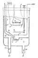
- An evacuable vessel is divided by a deck into an upper chamber U, evacuated by a diffusion pump DU throttled by a value VU, and a lower chamber L, evacuated by an independent diffusion pump DL throttled by a valve VL.
- the deck includes a water-cooled copper hearth H, in which an ingot I is placed consisting of a 25 mm x 50 mm single crystal of p-type silicon containing 1.6 x 10 23 atoms of boron per cubic metre and having a resistivity of 0.1 ohm cm, as a material to constitute the film to be deposited.
- An electron gun G provides a focused primary electron beam through a slot between the chambers to melt the ingot I.
- Stainless steel pipes P controlled by needle valves carry gases (Ar and H 2 ) into the upper chamber U to the vicinity of the surface of the molten ingot.
- a circular electrode E of stainless steel wire is positioned just above the hearth H and has a diameter approximately equal to that of the mouth of the hearth. A positive voltage can be applied to this electrode to ionise the gas.
- a shutter B screens a substrate S on which the film is to be deposited from the material (ingot I) in the hearth H until deposition is required.
- a holder for the substrate S is insulated from earth and carries a thermocouple T to measure its temperature except when bias is applied to the substrate, when the thermocouple must be removed to avoid shorting the bias to earth.
- the holder may however be earthed through a digital voltmeter DVM, which acts as an auto-bias resistor biassing the substrate such that the ion current flowing to it from the ionised gas (to be described) is negligibly small.
- a power supply e.g. of radio frequency can be substituted for the voltmeter DVM to regulate the substrate voltage and hence the ion bombardment of the substrate, as will be described.
- Adjustable infrared radiation heaters A provide for heating of the substrate.
- a glass slide typically Corning 7059 glass, is ultrasonically cleaned in an amphiphilic detergent, distilled water and isopropyl alcohol as conventional and then mounted in the substrate holder to act as the substrate S.
- the shutter B is placed to block the substrate's view of the ingot I (source) and the heaters A are turned on to give a substrate temperature of 250°C.
- the system is pumped down to a pressure of about 10 mB in both chambers U and L and the primary electron beam (from the gun G) is slowly turned up to a power of 2kW.
- the needle valves in the pipes P are opened to provide a flow of 30 millilitres per minute (mlm) of hydrogen.
- the valve VU controlling the evacuation of the upper chamber U is now slightly closed, to give a total pressure in this chamber of 2 x 10 -3 mB.
- the pressure in the lower chamber L which is more vigorously pumped, does not exceed 5 x 10 -4 mB; this is necessary to prevent extinction of the electron beam from the gun G, which depends for operation on an atmosphere sufficiently rarefied not to strike an arc at a field of 16kV/mm.
- a voltage of +400 volts is then applied to the electrode E and an ionisation current of about 0.1A flows.
- the substrate S develops a self-bias of about +350V with an ion current of about 0.1 A flowing to it.
- the shutter B is opened for 3 minutes causing a hydrogenated, boron-doped, p-type amorphous silicon film of thickness about 1.0 ⁇ m to be deposited on the glass substrate; typically the film has a p-type resistivity of 10 6 ohm cm, with a boron (acceptor) concentration of around 10 23 boron atoms per cubic metre and with a density of around 10 22 traps/cubic metre.
- a radio frequency power supply is installed at the site DVM.
- the source (the ingot I) is intrinsic silicon (i.e. undoped silicon).
- an r.f. bias of -1500V is applied to the substrate S; the flow of current to the electrode E thus rises to 0.5A.
- the shutter B is opened for 5 minutes causing a hydrogenated, p-type amorphous silicon film of thickness about 0.5 ⁇ m to be deposited on the glass substrate.
- the net rate of deposition in this option is somewhat lower.
- the film has a resistivity of 10 10 ohm cm at room temperature and a photoconductivity ratio of 10 5 when illuminated with AM1 sunlight.
- the film was annealed in the upper chamber U under a vacuum of 10 -5 mB for 3 hours at 200°C followed by cooling in vacuum, in both options.
Landscapes
- Chemical & Material Sciences (AREA)
- Chemical Kinetics & Catalysis (AREA)
- Engineering & Computer Science (AREA)
- Materials Engineering (AREA)
- Mechanical Engineering (AREA)
- Metallurgy (AREA)
- Organic Chemistry (AREA)
- Physical Deposition Of Substances That Are Components Of Semiconductor Devices (AREA)
- Physical Vapour Deposition (AREA)
- Physical Or Chemical Processes And Apparatus (AREA)
Applications Claiming Priority (2)
| Application Number | Priority Date | Filing Date | Title |
|---|---|---|---|
| GB8227776 | 1982-09-29 | ||
| GB8227776 | 1982-09-29 |
Publications (3)
| Publication Number | Publication Date |
|---|---|
| EP0104916A2 true EP0104916A2 (fr) | 1984-04-04 |
| EP0104916A3 EP0104916A3 (en) | 1984-12-27 |
| EP0104916B1 EP0104916B1 (fr) | 1987-04-08 |
Family
ID=10533249
Family Applications (1)
| Application Number | Title | Priority Date | Filing Date |
|---|---|---|---|
| EP83305705A Expired EP0104916B1 (fr) | 1982-09-29 | 1983-09-23 | Dépôt d'un film sur un substrat par évaporation à l'aide d'un faisceau d'électrons |
Country Status (5)
| Country | Link |
|---|---|
| US (1) | US4698235A (fr) |
| EP (1) | EP0104916B1 (fr) |
| JP (1) | JPS5987040A (fr) |
| DE (1) | DE3370829D1 (fr) |
| GB (2) | GB8324779D0 (fr) |
Cited By (4)
| Publication number | Priority date | Publication date | Assignee | Title |
|---|---|---|---|---|
| EP0184917A1 (fr) * | 1984-12-13 | 1986-06-18 | Stc Plc | Vase de réacteur à plasma et procédé |
| EP0209972A1 (fr) * | 1985-06-05 | 1987-01-28 | Plessey Overseas Limited | Procédé pour le dépôt d'un carbure de germanium hydrogéné |
| EP0161088B1 (fr) * | 1984-05-02 | 1988-06-08 | Energy Conversion Devices, Inc. | Appareil pour le dépôt de couches minces à l'aide de plasma |
| EP1055744A3 (fr) * | 1999-05-14 | 2007-07-04 | Neomax Co., Ltd. | Procédé de traitement de surface, appareillage de traitement de surface, matériau pour dépôt par vaporisation et aimant permanent à base de terre rare ayant une surface traitée |
Families Citing this family (6)
| Publication number | Priority date | Publication date | Assignee | Title |
|---|---|---|---|---|
| US4806431A (en) * | 1985-06-24 | 1989-02-21 | Lockheed Missiles & Space Company, Inc. | Composites coated with boron-silicon-oxide films |
| GB2182350B (en) * | 1985-07-01 | 1989-04-26 | Atomic Energy Authority Uk | Coating improvements |
| JP3433760B2 (ja) * | 1993-05-14 | 2003-08-04 | ソニー株式会社 | 光ディスクの保護膜機 |
| US5558720A (en) * | 1996-01-11 | 1996-09-24 | Thermacore, Inc. | Rapid response vapor source |
| ITRM20010060A1 (it) * | 2001-02-06 | 2001-05-07 | Carlo Misiano | Perfezionamento di un metodo e apparato per la deposizione di film sottili, soprattutto in condizioni reattive. |
| KR20040039012A (ko) * | 2002-10-30 | 2004-05-10 | 주식회사 실트론 | 실리콘 잉곳의 성장 장치 |
Family Cites Families (22)
| Publication number | Priority date | Publication date | Assignee | Title |
|---|---|---|---|---|
| US2784115A (en) * | 1953-05-04 | 1957-03-05 | Eastman Kodak Co | Method of producing titanium dioxide coatings |
| US2932588A (en) * | 1955-07-06 | 1960-04-12 | English Electric Valve Co Ltd | Methods of manufacturing thin films of refractory dielectric materials |
| US2930002A (en) * | 1957-06-24 | 1960-03-22 | Rca Corp | Oscillator |
| US3063871A (en) * | 1959-10-23 | 1962-11-13 | Merck & Co Inc | Production of semiconductor films |
| US3333639A (en) * | 1964-11-27 | 1967-08-01 | John S Page | Parallel string installation for single-zone production |
| US3617375A (en) * | 1969-08-11 | 1971-11-02 | Texas Instruments Inc | Electron beam evaporated quartz insulating material process |
| US3791852A (en) * | 1972-06-16 | 1974-02-12 | Univ California | High rate deposition of carbides by activated reactive evaporation |
| US3984581A (en) * | 1973-02-28 | 1976-10-05 | Carl Zeiss-Stiftung | Method for the production of anti-reflection coatings on optical elements made of transparent organic polymers |
| US3953652A (en) * | 1973-04-05 | 1976-04-27 | Itek Corporation | Process for coating glass onto polymeric substrates |
| GB1500701A (en) * | 1974-01-24 | 1978-02-08 | Atomic Energy Authority Uk | Vapour deposition apparatus |
| US4006268A (en) * | 1975-03-17 | 1977-02-01 | Airco, Inc. | Vapor collimation in vacuum deposition of coatings |
| CH610013A5 (fr) * | 1975-11-19 | 1979-03-30 | Battelle Memorial Institute | |
| CA1102013A (fr) * | 1977-05-26 | 1981-05-26 | Chin-An Chang | Traduction non-disponible |
| US4217374A (en) * | 1978-03-08 | 1980-08-12 | Energy Conversion Devices, Inc. | Amorphous semiconductors equivalent to crystalline semiconductors |
| DE2812311C2 (de) * | 1978-03-21 | 1986-10-09 | Leybold-Heraeus GmbH, 5000 Köln | Verfahren zum gleichzeitigen Vakuumaufdampfen dünner Schichten auf mehrere Substrate mittels Elektronenstrahlen und Anwendung auf die Bedampfung von Turbinenschaufeln |
| JPS5669819A (en) * | 1979-11-12 | 1981-06-11 | Canon Inc | Manufacture of amorphous silicon hydride layer |
| EP0029747A1 (fr) * | 1979-11-27 | 1981-06-03 | Konica Corporation | Installation pour le dépôt par vaporisation sous vide et procédé pour former une couche mince en utilisant cette installation |
| JPS5678112A (en) * | 1979-11-30 | 1981-06-26 | Toshiba Corp | Cutting and rounding device of metal wire |
| JPS5691437A (en) * | 1979-12-26 | 1981-07-24 | Nippon Hoso Kyokai <Nhk> | Preparation of metallized element |
| JPS5698819A (en) * | 1980-01-09 | 1981-08-08 | Nec Corp | Method of preparing thin film of amorphous silicon |
| US4297387A (en) * | 1980-06-04 | 1981-10-27 | Battelle Development Corporation | Cubic boron nitride preparation |
| IE53485B1 (en) * | 1981-02-12 | 1988-11-23 | Energy Conversion Devices Inc | Improved photoresponsive amorphous alloys |
-
1983
- 1983-09-15 GB GB838324779A patent/GB8324779D0/en active Pending
- 1983-09-22 JP JP58176107A patent/JPS5987040A/ja active Pending
- 1983-09-22 US US06/534,866 patent/US4698235A/en not_active Expired - Fee Related
- 1983-09-23 EP EP83305705A patent/EP0104916B1/fr not_active Expired
- 1983-09-23 DE DE8383305705T patent/DE3370829D1/de not_active Expired
- 1983-09-23 GB GB08325495A patent/GB2127438B/en not_active Expired
Cited By (4)
| Publication number | Priority date | Publication date | Assignee | Title |
|---|---|---|---|---|
| EP0161088B1 (fr) * | 1984-05-02 | 1988-06-08 | Energy Conversion Devices, Inc. | Appareil pour le dépôt de couches minces à l'aide de plasma |
| EP0184917A1 (fr) * | 1984-12-13 | 1986-06-18 | Stc Plc | Vase de réacteur à plasma et procédé |
| EP0209972A1 (fr) * | 1985-06-05 | 1987-01-28 | Plessey Overseas Limited | Procédé pour le dépôt d'un carbure de germanium hydrogéné |
| EP1055744A3 (fr) * | 1999-05-14 | 2007-07-04 | Neomax Co., Ltd. | Procédé de traitement de surface, appareillage de traitement de surface, matériau pour dépôt par vaporisation et aimant permanent à base de terre rare ayant une surface traitée |
Also Published As
| Publication number | Publication date |
|---|---|
| US4698235A (en) | 1987-10-06 |
| EP0104916B1 (fr) | 1987-04-08 |
| GB2127438A (en) | 1984-04-11 |
| GB2127438B (en) | 1986-07-30 |
| JPS5987040A (ja) | 1984-05-19 |
| EP0104916A3 (en) | 1984-12-27 |
| GB8324779D0 (en) | 1983-10-19 |
| GB8325495D0 (en) | 1983-10-26 |
| DE3370829D1 (en) | 1987-05-14 |
Similar Documents
| Publication | Publication Date | Title |
|---|---|---|
| US4336277A (en) | Transparent electrical conducting films by activated reactive evaporation | |
| CA1329791C (fr) | Procede de production de pellicules composites constituees de diamant, de diamant dope et de nitrure de bore cubique | |
| US4402762A (en) | Method of making highly stable modified amorphous silicon and germanium films | |
| US5055319A (en) | Controlled high rate deposition of metal oxide films | |
| Harper et al. | Quantitative ion beam process for the deposition of compound thin films | |
| US4376688A (en) | Method for producing semiconductor films | |
| US4596645A (en) | Reactively-sputtered zinc semiconductor films of high conductivity for heterojunction devices | |
| EP0479907A1 (fr) | Procede de production de pellicules en diamant, en diamant dope et des pellicules composites en diamant et en nitrure de bore cubique a basse temperature | |
| US4637869A (en) | Dual ion beam deposition of amorphous semiconductor films | |
| US6388366B1 (en) | Carbon nitride cold cathode | |
| JP2002504061A (ja) | 被覆工作物を製造するための方法、その方法の利用およびそのための装置 | |
| US6069436A (en) | Boron nitride cold cathode | |
| EP0104916A2 (fr) | Dépôt d'un film sur un substrat par évaporation à l'aide d'un faisceau d'électrons | |
| JPH06326024A (ja) | 半導体基板の製造方法及び非晶質堆積膜の形成方法 | |
| US5723034A (en) | Process for forming hydrogenated amorphous silicon film | |
| JPH0143449B2 (fr) | ||
| US4534840A (en) | Method for forming a compound semiconductor film | |
| US3463715A (en) | Method of cathodically sputtering a layer of silicon having a reduced resistivity | |
| US4266984A (en) | Enhanced open circuit voltage in amorphous silicon photovoltaic devices | |
| JP2001506572A (ja) | 気相合成によるダイヤモンド皮膜の形成方法 | |
| Takagi et al. | Film formation technique by ionized-cluster beam | |
| EP0177115B1 (fr) | Dépôt de films semi-conducteurs amorphes au moyen de deux faisceaux ioniques | |
| JPH079059B2 (ja) | 炭素薄膜の製造方法 | |
| RU2769751C1 (ru) | Устройство для нанесения сверхтолстых слоев поликристаллического кремния | |
| Kasdan et al. | Ion bombardment control of morphology during the growth of hydrogenated amorphous silicon thin films by reactive ion beam deposition |
Legal Events
| Date | Code | Title | Description |
|---|---|---|---|
| PUAI | Public reference made under article 153(3) epc to a published international application that has entered the european phase |
Free format text: ORIGINAL CODE: 0009012 |
|
| AK | Designated contracting states |
Designated state(s): DE FR GB NL |
|
| PUAL | Search report despatched |
Free format text: ORIGINAL CODE: 0009013 |
|
| AK | Designated contracting states |
Designated state(s): DE FR GB NL |
|
| 17P | Request for examination filed |
Effective date: 19841217 |
|
| GRAA | (expected) grant |
Free format text: ORIGINAL CODE: 0009210 |
|
| AK | Designated contracting states |
Kind code of ref document: B1 Designated state(s): DE FR GB NL |
|
| REF | Corresponds to: |
Ref document number: 3370829 Country of ref document: DE Date of ref document: 19870514 |
|
| ET | Fr: translation filed | ||
| PLBE | No opposition filed within time limit |
Free format text: ORIGINAL CODE: 0009261 |
|
| STAA | Information on the status of an ep patent application or granted ep patent |
Free format text: STATUS: NO OPPOSITION FILED WITHIN TIME LIMIT |
|
| 26N | No opposition filed | ||
| PGFP | Annual fee paid to national office [announced via postgrant information from national office to epo] |
Ref country code: GB Payment date: 19900814 Year of fee payment: 8 |
|
| PGFP | Annual fee paid to national office [announced via postgrant information from national office to epo] |
Ref country code: FR Payment date: 19900830 Year of fee payment: 8 |
|
| PGFP | Annual fee paid to national office [announced via postgrant information from national office to epo] |
Ref country code: DE Payment date: 19900928 Year of fee payment: 8 |
|
| PGFP | Annual fee paid to national office [announced via postgrant information from national office to epo] |
Ref country code: NL Payment date: 19900930 Year of fee payment: 8 |
|
| PG25 | Lapsed in a contracting state [announced via postgrant information from national office to epo] |
Ref country code: GB Effective date: 19910923 |
|
| PG25 | Lapsed in a contracting state [announced via postgrant information from national office to epo] |
Ref country code: NL Effective date: 19920401 |
|
| NLV4 | Nl: lapsed or anulled due to non-payment of the annual fee | ||
| GBPC | Gb: european patent ceased through non-payment of renewal fee | ||
| PG25 | Lapsed in a contracting state [announced via postgrant information from national office to epo] |
Ref country code: FR Effective date: 19920529 |
|
| PG25 | Lapsed in a contracting state [announced via postgrant information from national office to epo] |
Ref country code: DE Effective date: 19920602 |
|
| REG | Reference to a national code |
Ref country code: FR Ref legal event code: ST |