EP0106222A2 - Halbleiterspeicheranordnung - Google Patents
Halbleiterspeicheranordnung Download PDFInfo
- Publication number
- EP0106222A2 EP0106222A2 EP83109635A EP83109635A EP0106222A2 EP 0106222 A2 EP0106222 A2 EP 0106222A2 EP 83109635 A EP83109635 A EP 83109635A EP 83109635 A EP83109635 A EP 83109635A EP 0106222 A2 EP0106222 A2 EP 0106222A2
- Authority
- EP
- European Patent Office
- Prior art keywords
- power source
- source voltage
- voltage
- mos transistor
- semiconductor memory
- Prior art date
- Legal status (The legal status is an assumption and is not a legal conclusion. Google has not performed a legal analysis and makes no representation as to the accuracy of the status listed.)
- Granted
Links
- 239000004065 semiconductor Substances 0.000 title claims abstract description 55
- 230000003068 static effect Effects 0.000 claims abstract description 23
- 239000002245 particle Substances 0.000 description 10
- 239000003990 capacitor Substances 0.000 description 4
- 230000035945 sensitivity Effects 0.000 description 4
- 238000010586 diagram Methods 0.000 description 3
- 229910044991 metal oxide Inorganic materials 0.000 description 2
- 150000004706 metal oxides Chemical class 0.000 description 2
- 229910052776 Thorium Inorganic materials 0.000 description 1
- 229910052770 Uranium Inorganic materials 0.000 description 1
- 230000000295 complement effect Effects 0.000 description 1
- 230000006378 damage Effects 0.000 description 1
- 238000013500 data storage Methods 0.000 description 1
- 230000006870 function Effects 0.000 description 1
- 239000012535 impurity Substances 0.000 description 1
- 239000000463 material Substances 0.000 description 1
- 238000005259 measurement Methods 0.000 description 1
- 230000002285 radioactive effect Effects 0.000 description 1
Images


Classifications
-
- G—PHYSICS
- G11—INFORMATION STORAGE
- G11C—STATIC STORES
- G11C5/00—Details of stores covered by group G11C11/00
- G11C5/14—Power supply arrangements, e.g. power down, chip selection or deselection, layout of wirings or power grids, or multiple supply levels
- G11C5/141—Battery and back-up supplies
-
- G—PHYSICS
- G11—INFORMATION STORAGE
- G11C—STATIC STORES
- G11C11/00—Digital stores characterised by the use of particular electric or magnetic storage elements; Storage elements therefor
- G11C11/21—Digital stores characterised by the use of particular electric or magnetic storage elements; Storage elements therefor using electric elements
- G11C11/34—Digital stores characterised by the use of particular electric or magnetic storage elements; Storage elements therefor using electric elements using semiconductor devices
- G11C11/40—Digital stores characterised by the use of particular electric or magnetic storage elements; Storage elements therefor using electric elements using semiconductor devices using transistors
- G11C11/41—Digital stores characterised by the use of particular electric or magnetic storage elements; Storage elements therefor using electric elements using semiconductor devices using transistors forming static cells with positive feedback, i.e. cells not needing refreshing or charge regeneration, e.g. bistable multivibrator or Schmitt trigger
- G11C11/413—Auxiliary circuits, e.g. for addressing, decoding, driving, writing, sensing, timing or power reduction
- G11C11/417—Auxiliary circuits, e.g. for addressing, decoding, driving, writing, sensing, timing or power reduction for memory cells of the field-effect type
Definitions
- This invention relates to a static type semiconductor memory device.
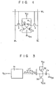
- Fig. 1 shows a circuit diagram of a general semiconductor memory device.
- reference numerals 1 and 2 respectively designate MOS (metal oxide semiconductor) transistors constituting a flip-flop 7; numerals 3 and 4 indicate MOS transistors serving as transfer gates; and numerals 5 and 6 are high resistance elements as loads.
- V CC denotes a power source voltage and V ss a reference voltage, which is ground in this instance.
- BL and BL denote bit lines (data input/output lines), respectively, and WL indicates a word line.
- the memory cell thus arranged employs a commercial power source of approximately 100 V for supplying the power source voltage V CC in an operation mode, i.e. a read mode or a write mode.
- the memory cell is supplied with a voltage which is formed by dropping the commerical power source voltage to about 5 V via a transformer.
- the power source voltage V CC is switched from the commerical power source to a battery of approximately 2.5 V. This is called a battery back-up system and is widely used for data-holding in this field.
- a specific data error In the static type semiconductor memory device, a specific data error, called a soft error, has recently become a focus of concern. This phenomenon arises from alpha particles emitted from radioactive impurities contained in the material of the package or the memory chip, for example, U and Th. When the alpha particles enter the memory chip, electron-hole pairs are generated and a current from these pairs flows into data-storing nodes, resulting in destruction of data stored in those nodes.
- the soft error observed in the static type semiconductor memory device will be described referring to Fig. 1.
- a current due to the electron-hole pairs flows through the memory cell to pull down the potential on a high potential node of the flip-flop 7 (either of the output nodes N1 or N2 of the MOS transistors 1 and 2), thereby destroying the logical state "1" or "0" of the flip-flop 7.
- the nodes N1 and N2 of the flip-flop 7 are connected to the power source voltage V CC through the high resistance loads 5 and 6.
- the high potential node is equivalent to a floating state.
- the capacitance on the nodes of the static type semiconductor memory device is smaller than that of the dynamic type semiconductor memory device. Therefore, the soft error problem in the static type semiconductor memory device is more serious than in the dynamic type semiconductor memory device.
- the applied voltage when the semiconductor memory device is backed up by the battery in a wait mode, is generally about 2.5 V.
- the quantity of charges stored in the data storing node is reduced by half, as compared with that when the semiconductor memory device is in an operation mode with an applied voltage of approximately 5 V. Therefore, the semiconductor memory device is more sensitive to the alpha particles when it is in the battery back-up mode. This implies that the sensitivity of the static type semiconductor memory device to alpha particles is greatly determined by the sensitivity of the semiconductor memory device when it is in a battery back-up mode. Consequently, in order to solve the soft error problem, it is necessary to render the semiconductor memory device more insensitive-to alpha particles when it is in a battery back-up mode.
- an object of the present invention is to provide a static type semiconductor memory device which is substantially free from soft errors, with a considerably lessened sensitivity to alpha particles, particularly in a battery back-up mode.
- a static type semiconductor memory device comprising means for boosting a power source voltage, and a static memory cell for receiving the output voltage from said boosting circuit as a power source voltage.
- FIG. 2 there is shown an embodiment of a static type semiconductor memory device according to this invention.
- reference numeral 11 designates a boosting circuit which receives the power source voltage V CC and boosts it to an output voltage V CCX ;
- numeral 12 indicates a switch circuit which receives the output voltage V ccx from the boosting circuit 11 and the power source voltage V CC and selects one of those voltages;
- numeral 13 is a static type semiconductor memory device which receives the selected power source voltage V CCS from the switch circuit 12 as a power source voltage.
- the boosting circuit 11 boosts the power source voltage V CC of 2.5 V, for example, to a voltage of 4 V, for example. This circuit will be described in detail later with reference to Fig. 3.
- the switch circuit 12 is comprised of two input terminals 14 and 15 and a select contact 16, as schematically illustrated in Fig. 2. The details of this circuit will be given later referring to Fig. 4.
- the input terminal 14 receives the output voltage V ccx from the boosting circuit 11 and the input terminal 15 receives the power source voltage V CC .
- the select contact 16, constituting a power source terminal of the switch circuit 12 is connected to a power source terminal TS.
- the output voltage V CCX or V CC selected by the switch circuit 12 is applied as a power source voltage V CCS to the semiconductor memory cell 13.
- the semiconductor memory cell 13 is composed of a pair of enhancement type N-channel MOS transistors 18 and 19, enhancement type N-channel MOS transistors 20 and 21 as transfer gates, and high resistance elements 22 and 23 as loads.
- the gate of the MOS transistor 18 is connected to the drain of the MOS transistor 19.
- the gate of the MOS transistor 19 is connected to the drain of the MOS transistor 18.
- the sources of both the MOS transistors 18 and 19 are connected to the reference voltage V SS , which is ground in this instance.
- the drain of the MOS transistor 18 is connected to the power source terminal TS via the load 22.
- the drain of the MOS transistor 19 is likewise connected to the power source terminal TS via the load 23.
- a MOS transistor 20 as a transfer gate is inserted between the drain of the MOS transistor 18 and the bit line BL. Inserted between the drain of the MOS transistor 19 and the bit line BL is a MOS transistor 21 as a transfer gate.
- the gates of the MOS transistors 20 and 21 are both connected to the word line WL.
- the drains of the MOS transistors 18 and 19 provide data-storing nodes N18 and N19, respectively.
- the word line WL is selected, i.e., it is logical "1".
- the commerical power source is used for the power source of this semiconductor memory device.
- a 5 V voltage formed by dropping the commerical power source voltage is used for the power source voltage V cc .
- the 5 V voltage is applied to the power source terminal of the boosting circuit 11 and the input terminal 15 of the switch circuit 12.
- the select contact 16 of the switch circuit 12 is connected to the input terminal 15, and the power source voltage V CC is thereby selected.
- the power source voltage V CC of approximately 5 V is directly applied as the power source voltage V CCS to the power source terminal TS of the semiconductor memory cell 13.
- the word line WL is selected, that is, it has a logical state of "1".
- data of logical "1" and "0” or logical "0” and “1” are respectively written into or read out from the nodes N18 and N19 through the bit lines BL and BL and the transfer gate MOS transistors 20 and 21.
- the power source is switched from the commerical power source to the battery, so that the battery supplies a voltage of approximately 2.5 V as the power source voltage V cC .
- the select contact 16 of the switch circuit 12 is connected to the input terminal 14 to select the output voltage V CCX from the boosting circuit 11.
- the output voltage V ccx from the boosting circuit 11 is applied as the power source voltage V CCS to the power source terminal Ts of the semiconductor memory cell 13.
- the boosting circuit 11 is used to boost the power source voltage V CC from approximately 2.5 V to approximately 4 V. This will be discussed in more detail later.
- the boosted output voltage V CCX of approximately 4 V is applied to the power source terminal TS of the semiconductor memory cell 13 as the power source voltage V CC .
- the rate of soft error occurrence was measured using the conventional memory cell as shown in Fig. 1.
- alpha particles are radiated onto the memory chip while the semiconductor memory device is in a wait mode.
- the measured results showed that when the power source voltage V Cc of approximately 4 V was applied, the rate of soft error occurrence was considerably reduced, as compared with the case where the power source voltage V CC was approximately 2.5 V.
- These results also showed that the sensitivity of the semiconductor memory device of this embodiment when the approximately 4 V, for example, in the wait mode, was reduced to at least one-tenth that of the conventional semiconductor memory device.
- Fig. 3 shows an example of the practical arrangement of the boosting circuit 11 in the semiconductor memory device of Fig. 2.
- Reference numeral 31 denotes a ring oscillator containing an odd number of inverters cascade-connected in a ring fashion (not shown).
- the power source voltage V CC is applied to the ring oscillator 31.
- the ring oscillator 31 produces an output signal of the voltage V CC and frequency f..
- the output terminal of the ring oscillator 31 is connected to one electrode of a capacitor C.
- the capacitor C receives at this electrode the output voltage of the frequency f.
- the other electrode of the capacitor C is connected to the source of an enhancement type N-channel MOS transistor 32 whose drain is connected to the power source voltage V CC .
- the drain and gate of the MOS transistor 32 are interconnected.
- the drain of an N-channel MOS,transistor of enhancement type is connected to the source of the MOS transistor 32.
- the source of the MOS transistor 33 serves as an output terminal from which the boosted output voltage V ccx is taken out.
- the gate of the MOS transistor 33 is connected to the drain thereof.
- a stray capacitance Cp is present between the source interjunction of the MOS transistor 32 with the MOS transistors 33 and the ground.
- the output voltage V ccx is independent of the frequency f and is given as
- Equation (1) is rewritten as where V T designates the threshold voltage V T of the MOS transistors 32 and 33.
- the output voltage V CCX is 5 V.
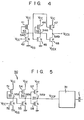
- Fig. 4 shows a practical arrangement of the switch circuit 12.
- An N-channel depletion type MOS transistor 41 and an N-channel enhancement type MOS transistor 42 make up a first inverter 43.
- An N-channel depletion type MOS transistor 44 and an N-channel enhancement type MOS transistor 45 form a second inverter 46.
- the drain of the MOS transistor 41 is connected to the power source voltage V CC and its source is connected to the drain of the MOS transistor 42.
- the gate of the MOS transistor 41 is connected to its source.
- the power source voltage V CC is applied to the gate of the MOS transistor 42.
- the source of the MOS transistor 42 is connected to the reference voltage V SS (0 V).
- the drain of the MOS transistor 44 is connected to the power source voltage V CC and its source is connected to the drain of the MOS transistor 45.
- the gate of the MOS transistor 44 is coupled .with the source thereof.
- the source of the MOS transistor 45 is connected to the reference voltage V SS .
- the gate of the MOS transistor 45 is connected to an output node N43 of the inverter 43, i.e. the interjunction between the MOS transistors 41 and 42.
- the source of a P-channel enhancement type MOS transistor 47 is connected to the power source voltage V CC and its drain is connected to the drain of a P-channel enhancement type MOS transistor 48.
- the source of the MOS transistor 48 is applied with the output voltage Vccx from the boosting circuit 11.
- the junction between the MOS transistors 47 and 48 forms an output node N49 of the switch circuit 12, through which the power source voltage V CC or V CCX selected by the switch circuit 12 is taken out as the power source voltage V CCS .
- the gate of the MOS transistor 47 is connected to the output node N43 of the first inverter 43.
- the gate of the MOS transistor 48 is connected to the output node N46 of the second inverter 46, i.e., the junction between the MOS transistors 44 and 45.
- the threshold voltage V T of the MOS transistor 42 is approximately 3 V
- the threshold voltages V T of the MOS transistors 45, 47 and 48 is approximately 0.5 V, -0.5 V and -0.5 V, respectively.
- the applied power source voltage V Cc is 5 V.
- the MOS transistor 42 is turned on and the potential at the node N43 is 0 V.
- the MOS transistor 45 is turned off and the node N46 has a potential of 5 V.
- the MOS transistor 47 is turned on and the MOS transistor is turned off.
- the switch circuit 12 produces the power source voltage V Cc of approximately 5 V as the power source voltage V CCS through the MOS transistor 47.
- the data hold mode when the power source voltage V CC is approximately 2.5 V, the node N43 is at 2.5 V since the MOS transistor 42 is off. Then, the MOS transistor 45 is on and the node N46 is at 0 V.
- the MOS transistor 47 is off and the MOS transistor 48 is on. Consequently, the switch circuit 12 produces the power source voltage V CCS via the MOS transistor 48.
- the power source voltage V CCS is the output voltage V CCX of, for example, 4 V, from the boosting circuit 11.
- the voltages at the nodes N43, N46 and N49 against V Cc are indicated below.
- Fig. 5 there is shown an example of the power source circuit used in the boosting circuit shown in Fig. 3.
- the ring oscillator 31 is coupled with the output voltage V CCP of a power source circuit 50, while in the Fig. 3 arrangement, the ring oscillator 31 is directly coupled with the power source V CC .
- the circuit arrangement of Fig. 5 shows the boosting circuit 11 to operate only in the battery back-up mode.
- MOS transistors 51 and 54 are of N-channel and depletion type
- MOS transistors 52, 55 and 58 are N-channel and enhancement type.
- a MOS transistor 57 is of P-channel and enhancement type.
- the MOS transistors 51 and 52 make up an E/D (enhancement/depletion) inverter 53.
- the MOS transistors 54 and 55 likewise make up another E/D inverter 56.
- the MOS transistors 57 and 58 form a CMOS (complementary metal oxide semiconductor) inverter 59.
- the MOS transistor 51 is connected at the drain to the power source voltage V CC and at the source to the drain of the MOS transistor 52.
- the gate of the MOS transistor 51 is connected to its source.
- the MOS transistor 52 is connected at the source to the reference voltage V SS (0 V), and at the gate to the power source voltage V CC .
- the junction between the MOS transistors 51 and 52 provides an output node N53 of the inverter 53.
- the MOS transistor 54 is connected at the drain to the power source voltage V CC and at the source to the drain of the MOS transistor 55.
- the gate of the MOS transistor 54 is connected to its source.
- the source of the MOS transistor 55 is connected to the reference voltage V SS and the gate thereof is connected to the output node N53 of the inverter 53.
- the junction between the MOS transistors 54 and 55 provides an output node N56 of the inverter 56.
- the MOS transistor 57 is connected at the source to the power source voltage V CC and at the drain to the drain of the MOS transistor 58.
- the source of the MOS transistor 58 is coupled with the reference voltage V SS .
- the gates of the MOS transistors 57 and 58 are both connected to the output node N56 of the MOS transistor 56.
- the junction between the MOS transistors 57 and 58 provides an output node N59 of the inverter 59, and also provides an output terminal of the power source circuit 50.
- the threshold voltage V T of the MOS transistor 52 is approximately 3 V
- the threshold voltage V T of the MOS transistors 55 and 58 is approximately 0.5 V
- that of the MOS transistor 57 is -0.5 V.
- the MOS transistor 52 is turned on and a potential at the node N53 is 0 V. Then, the MOS transistor 55 is turned off and a potential at the node N56 is 5 V. Accordingly, the MOS transistor 57 is turned off and the MOS transistor 58 is turned on. As a result, at the output node N59 the output power source voltage V CCP becomes the reference voltage V SS , and this reference voltage V SS is applied to the ring oscillator 31 as the power source voltage to the boosting circuit 11. Specifically, when the power source voltage V ce is 5 V, 0 V is applied to the ring oscillator 31. The ring oscillator 31, and hence, the boosting circuit 11 will not operate.
- the power supply system of the semiconductor memory device is switched to the battery back-up system.
- the MOS transistor -52 is turned off and the node 53 has a potential of 2.5 V.
- the MOS transistor 55 is on and the node N56 is 0 V.
- the MOS transistor 57 is turned on and the MOS transistor 58 is turned off.
- the output power source voltage VCCP is the power source voltage V CC which is then applied to the ring oscillator 31.
- the output voltage V CCX for example, 4 V, of the switch circuit 12 is applied to the memory cell.
- the voltage applied to the ring oscillator 31 is 0 V when the power source voltage V CC is 5 V.
- the result is that the ring oscillator 31, and hence the boosting circuit 11, does not operate. Thus, power saving is achieved.
- Fig. 6 shows another embodiment of a semiconductor memory device according to this invention.
- the switch circuit 12, which is used in the embodiment of Fig. 3, is omitted.
- the output voltage V CCX of the boosting circuit 11 is directly connected to the power source terminal Ts of the memory cell 13.
- the remaining portion is the same as that of the Fig. 3 embodiment. No further explanation will be given and like reference numerals will be applied to like or equivalent portions.
- the output voltage V CCX boosted by the boosting circuit 11 is always applied to the memory cell 13.
- the semiconductor memory device is battery-driven with the V CC of 2.5 V in the wait mode
- the V ccx of about 4 V boosted by the boosting circuit 11 is applied to the memory cell 13. Therefore, this embodiment can prevent the soft error in the same way as the Fig. 3 embodiment does.
- the output voltage V CCX of the boosting circuit 11 is applied as the power source voltage to the semiconductor memory cell 13. Accordingly, this embodiment does not need the power source circuit 50 as shown in Fig. 5 which supplies the 0 V output voltage in an operation mode.
- the boosting circuit and the switch circuit may be replaced with any other circuits if these have the same functions as the former.
- the boosting circuit used in this invention sufficiently boosts the low voltage source when the semiconductor memory device is backed up by the battery in a wait mode.
- the boosted power source is applied to the memory cell in the wait mode. Therefore, the data storage in this mode is highly reliable.
- the semiconductor memory device of the invention is improved in its resistance to alpha particles and is thus substantially free from the soft error problem.
Landscapes
- Engineering & Computer Science (AREA)
- Power Engineering (AREA)
- Microelectronics & Electronic Packaging (AREA)
- Computer Hardware Design (AREA)
- Dram (AREA)
- Static Random-Access Memory (AREA)
Applications Claiming Priority (2)
| Application Number | Priority Date | Filing Date | Title |
|---|---|---|---|
| JP178804/82 | 1982-10-12 | ||
| JP57178804A JPS5968891A (ja) | 1982-10-12 | 1982-10-12 | 半導体メモリ |
Publications (3)
| Publication Number | Publication Date |
|---|---|
| EP0106222A2 true EP0106222A2 (de) | 1984-04-25 |
| EP0106222A3 EP0106222A3 (en) | 1986-01-22 |
| EP0106222B1 EP0106222B1 (de) | 1988-08-03 |
Family
ID=16054938
Family Applications (1)
| Application Number | Title | Priority Date | Filing Date |
|---|---|---|---|
| EP19830109635 Expired EP0106222B1 (de) | 1982-10-12 | 1983-09-27 | Halbleiterspeicheranordnung |
Country Status (3)
| Country | Link |
|---|---|
| EP (1) | EP0106222B1 (de) |
| JP (1) | JPS5968891A (de) |
| DE (1) | DE3377600D1 (de) |
Cited By (4)
| Publication number | Priority date | Publication date | Assignee | Title |
|---|---|---|---|---|
| WO1986004724A1 (en) * | 1985-02-08 | 1986-08-14 | American Telephone & Telegraph Company | Integrated circuit having a variably boosted node |
| EP0335008A1 (de) * | 1988-03-31 | 1989-10-04 | International Business Machines Corporation | Gegen weiche Fehler widerstandsfähige Datenspeicherzellen |
| EP0310351B1 (de) * | 1987-09-30 | 1993-07-14 | Texas Instruments Incorporated | Statischer Speicher in Schottky-Technologie |
| EP0211232B1 (de) * | 1985-07-01 | 1993-12-29 | Nec Corporation | Halbleiterspeicher mit einem Leseverfahren in einem grossen Speisespannungsbereich |
Families Citing this family (2)
| Publication number | Priority date | Publication date | Assignee | Title |
|---|---|---|---|---|
| JPH04256425A (ja) * | 1991-02-05 | 1992-09-11 | Nippon Millipore Kogyo Kk | ろ過用逆洗装置 |
| JP4198201B2 (ja) * | 1995-06-02 | 2008-12-17 | 株式会社ルネサステクノロジ | 半導体装置 |
Family Cites Families (4)
| Publication number | Priority date | Publication date | Assignee | Title |
|---|---|---|---|---|
| US4260909A (en) * | 1978-08-30 | 1981-04-07 | Bell Telephone Laboratories, Incorporated | Back gate bias voltage generator circuit |
| US4288865A (en) * | 1980-02-06 | 1981-09-08 | Mostek Corporation | Low-power battery backup circuit for semiconductor memory |
| JPS5712481A (en) * | 1980-06-26 | 1982-01-22 | Mitsubishi Electric Corp | Semiconductor memory device |
| JPS58161195A (ja) * | 1982-03-19 | 1983-09-24 | Fujitsu Ltd | スタテイツク型半導体記憶装置 |
-
1982
- 1982-10-12 JP JP57178804A patent/JPS5968891A/ja active Pending
-
1983
- 1983-09-27 DE DE8383109635T patent/DE3377600D1/de not_active Expired
- 1983-09-27 EP EP19830109635 patent/EP0106222B1/de not_active Expired
Cited By (4)
| Publication number | Priority date | Publication date | Assignee | Title |
|---|---|---|---|---|
| WO1986004724A1 (en) * | 1985-02-08 | 1986-08-14 | American Telephone & Telegraph Company | Integrated circuit having a variably boosted node |
| EP0211232B1 (de) * | 1985-07-01 | 1993-12-29 | Nec Corporation | Halbleiterspeicher mit einem Leseverfahren in einem grossen Speisespannungsbereich |
| EP0310351B1 (de) * | 1987-09-30 | 1993-07-14 | Texas Instruments Incorporated | Statischer Speicher in Schottky-Technologie |
| EP0335008A1 (de) * | 1988-03-31 | 1989-10-04 | International Business Machines Corporation | Gegen weiche Fehler widerstandsfähige Datenspeicherzellen |
Also Published As
| Publication number | Publication date |
|---|---|
| EP0106222A3 (en) | 1986-01-22 |
| EP0106222B1 (de) | 1988-08-03 |
| DE3377600D1 (en) | 1988-09-08 |
| JPS5968891A (ja) | 1984-04-18 |
Similar Documents
| Publication | Publication Date | Title |
|---|---|---|
| EP0594968B1 (de) | Gegen Soft-Fehler resistenter statischer Direktzugriffspeicher | |
| US4725981A (en) | Random access memory cell resistant to inadvertant change of state due to charged particles | |
| US4176289A (en) | Driving circuit for integrated circuit semiconductor memory | |
| US4682306A (en) | Self-refresh control circuit for dynamic semiconductor memory device | |
| KR0153847B1 (ko) | 반도체 기억장치 | |
| US6225852B1 (en) | Use of biased high threshold voltage transistor to eliminate standby current in low voltage integrated circuits | |
| IE54336B1 (en) | Volgate level detecting circuitry | |
| KR910000383B1 (ko) | 다이나믹형 랜덤억세스메모리 | |
| US4621346A (en) | Low power CMOS fuse circuit | |
| EP0168246B1 (de) | Aktive Erhöhungsschaltung | |
| EP0233968B1 (de) | Statische Speicherzelle ohne Taktgeber | |
| EP0106222B1 (de) | Halbleiterspeicheranordnung | |
| US5267192A (en) | Semiconductor memory device | |
| US3971004A (en) | Memory cell with decoupled supply voltage while writing | |
| US5640341A (en) | Memory cell insensitive to collisions of heavy ions | |
| US5260904A (en) | Data bus clamp circuit for a semiconductor memory device | |
| KR100417479B1 (ko) | 게인메모리셀용저전력센스증폭기 | |
| JP3841469B2 (ja) | 内部セル電圧を減少させたsramメモリセル | |
| EP0748535B1 (de) | Speisespannungsdetektorschaltung | |
| EP0204385A1 (de) | Nichtflüchtige programmierbare statische Speicherzelle und ein nichtflüchtiger programmierbarer statischer Speicher | |
| US4833343A (en) | Clock generator having complementary transistors | |
| US4469960A (en) | Voltage translating circuit | |
| US6618316B2 (en) | Pseudo-static single-ended cache cell | |
| KR0126908B1 (ko) | 스태틱형 반도체 메모리 디바이스 | |
| US4423340A (en) | Sense amplifier |
Legal Events
| Date | Code | Title | Description |
|---|---|---|---|
| PUAI | Public reference made under article 153(3) epc to a published international application that has entered the european phase |
Free format text: ORIGINAL CODE: 0009012 |
|
| 17P | Request for examination filed |
Effective date: 19831024 |
|
| AK | Designated contracting states |
Designated state(s): DE FR GB |
|
| RAP1 | Party data changed (applicant data changed or rights of an application transferred) |
Owner name: KABUSHIKI KAISHA TOSHIBA |
|
| PUAL | Search report despatched |
Free format text: ORIGINAL CODE: 0009013 |
|
| AK | Designated contracting states |
Designated state(s): DE FR GB |
|
| 17Q | First examination report despatched |
Effective date: 19870507 |
|
| GRAA | (expected) grant |
Free format text: ORIGINAL CODE: 0009210 |
|
| AK | Designated contracting states |
Kind code of ref document: B1 Designated state(s): DE FR GB |
|
| REF | Corresponds to: |
Ref document number: 3377600 Country of ref document: DE Date of ref document: 19880908 |
|
| ET | Fr: translation filed | ||
| PLBE | No opposition filed within time limit |
Free format text: ORIGINAL CODE: 0009261 |
|
| STAA | Information on the status of an ep patent application or granted ep patent |
Free format text: STATUS: NO OPPOSITION FILED WITHIN TIME LIMIT |
|
| 26N | No opposition filed | ||
| PGFP | Annual fee paid to national office [announced via postgrant information from national office to epo] |
Ref country code: FR Payment date: 19970909 Year of fee payment: 15 |
|
| PGFP | Annual fee paid to national office [announced via postgrant information from national office to epo] |
Ref country code: GB Payment date: 19970918 Year of fee payment: 15 |
|
| PGFP | Annual fee paid to national office [announced via postgrant information from national office to epo] |
Ref country code: DE Payment date: 19971010 Year of fee payment: 15 |
|
| PG25 | Lapsed in a contracting state [announced via postgrant information from national office to epo] |
Ref country code: GB Free format text: LAPSE BECAUSE OF NON-PAYMENT OF DUE FEES Effective date: 19980927 |
|
| GBPC | Gb: european patent ceased through non-payment of renewal fee |
Effective date: 19980927 |
|
| PG25 | Lapsed in a contracting state [announced via postgrant information from national office to epo] |
Ref country code: FR Free format text: LAPSE BECAUSE OF NON-PAYMENT OF DUE FEES Effective date: 19990531 |
|
| PG25 | Lapsed in a contracting state [announced via postgrant information from national office to epo] |
Ref country code: DE Free format text: LAPSE BECAUSE OF NON-PAYMENT OF DUE FEES Effective date: 19990701 |
|
| REG | Reference to a national code |
Ref country code: FR Ref legal event code: ST |