EP0106265A2 - Appareil de traitement de données d'image - Google Patents
Appareil de traitement de données d'image Download PDFInfo
- Publication number
- EP0106265A2 EP0106265A2 EP83109915A EP83109915A EP0106265A2 EP 0106265 A2 EP0106265 A2 EP 0106265A2 EP 83109915 A EP83109915 A EP 83109915A EP 83109915 A EP83109915 A EP 83109915A EP 0106265 A2 EP0106265 A2 EP 0106265A2
- Authority
- EP
- European Patent Office
- Prior art keywords
- image data
- parameter
- original image
- processing apparatus
- storage means
- Prior art date
- Legal status (The legal status is an assumption and is not a legal conclusion. Google has not performed a legal analysis and makes no representation as to the accuracy of the status listed.)
- Granted
Links
Images


Classifications
-
- G—PHYSICS
- G06—COMPUTING OR CALCULATING; COUNTING
- G06T—IMAGE DATA PROCESSING OR GENERATION, IN GENERAL
- G06T5/00—Image enhancement or restoration
- G06T5/20—Image enhancement or restoration using local operators
-
- Y—GENERAL TAGGING OF NEW TECHNOLOGICAL DEVELOPMENTS; GENERAL TAGGING OF CROSS-SECTIONAL TECHNOLOGIES SPANNING OVER SEVERAL SECTIONS OF THE IPC; TECHNICAL SUBJECTS COVERED BY FORMER USPC CROSS-REFERENCE ART COLLECTIONS [XRACs] AND DIGESTS
- Y10—TECHNICAL SUBJECTS COVERED BY FORMER USPC
- Y10S—TECHNICAL SUBJECTS COVERED BY FORMER USPC CROSS-REFERENCE ART COLLECTIONS [XRACs] AND DIGESTS
- Y10S378/00—X-ray or gamma ray systems or devices
- Y10S378/901—Computer tomography program or processor
Definitions
- the present invention relates to an image data processing apparatus which performs spatial filtering of image data so as to extract and display image data effective for diagnosis by a physician in a medical image diagnosis apparatus.
- Digital signal processing techniques are more frequently being used in medical image processing by medical image processing apparatuses such as X-ray CT apparatuses or digital radiography apparatuses.
- medical image processing apparatuses such as X-ray CT apparatuses or digital radiography apparatuses.
- spatial filtering has an important role as a technique for performing smoothening, or edge enhancement.
- a digital radiography apparatus for obtaining an X-ray transmission image in the form of digital data has a density resolution of 200 to 500 tone or gradation (gray) levels.
- a display device e.g., a CRT has only about 30 gradation levels.
- a viewer has the ability to distinguish about 10 to 20 gradation levels. For this reason, there have been many types of image data which are included in the original image data and which are effective for diagnosis and yet which cannot be used for reproducing fine contrast.
- an image data processing apparatus comprising first storage means for storing original image data in a digital form which is used for medical diagnosis, filtering means for performing a filtering function of said original image data so as to control spatial frequency characteristics of said original image data, second storage means for storing the filtered image data derived from said filtering means, first multiplier means for multiplying said filtered image data which is stored in said second storage means, by a first parameter so as to give a first weighted value to said filtered image data, second multiplier means for multiplying said original image data which is stored in said first storage means, by a second parameter so as to give a second weighted value to said original image data, parameter input terminal means for producing said two parameters and delivering the same to said first and second multiplier means respectively, and adder means for performing a linear combination operation between said first and second multiplied image data so as to obtain an added image data whose spatial frequency characteristics are controlled to be different from that of said original image data.
- an original image data storage memory (referred to as "OID" memory) 1 stores digital image data obtained by scanning an object (not shown) by a known digital radiography apparatus or the like.
- An output from the OID memory 1 is connected to a 3 x 3 filter 2 and to a multiplier 5 having a multiplication of B.
- the filter 2 performs a filtering process to be described later.
- An output from the filter 2 is supplied to a filtered image data storage memory (referred to as "FID" memory) 3 and is stored therein.
- An output from the FID memory 3 is supplied to a multiplier 4 having a multiplication of A.
- An output from a parameter input terminal 8 is used for controlling the two multipliers 4 and 5 described above. Outputs from the multipliers 4 and 5 are supplied to an image data adder device (referred to as "adder device”) 6 which performs a linear combination to be described later. The sum image data from the adder device 6 is accumulated in a processed image data storage memory (referred to as "PID" memory) 7.
- PID processed image data storage memory
- the filter 2 performs the filtering process of smoothening or enhancing the original image data stored in the OID memory 1.
- the filtered image data from the filter 2 is stored in the FID memory 3.
- the filtered image data stored in the FID memory 3 is multiplied by A by the first multiplier 4, and the multiplication product is supplied to the image data adder device 6.
- the original image data from the OID memory 1 is multiplied by B by the second multiplier 5 and the multiplication product is supplied to the adder device 6.
- the filter 2 is a basic and important device in image processing and is effective for noise removal, sharpness control, edge enhancement and the like.
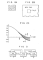
- a 3 x 3 filter is a filter which performs a convolution given by equation (1) below between a matrix of coefficients a, b and c as shown in Fig. 2A and one input pixel (x, y) as shown in Fig. 2B.
- the spatial frequency characteristics in the x- and y-directions of a 3 x 3 filter having such filter coefficients a, b and c are designated by u and v
- the spatial frequency characteristics of the filter can be given by:
- this filter can be used as either a low-pass filter or a high-pass filter.
- equation (3) can be rewritten as equation (7) below:
- the filter serves as a low-pass filter.
- the parameter B defines the ratio of the component of the original image data in the output data. The greater the parameter B, the closer the output image data is to the original image data. The smaller the parameter B, the more significant are the high-pass or low-pass characteristics of the filter. In this manner, the two parameters A and B are significant values in determining the filter characteristics, and can be conveniently used as a measure for determining the spatial frequency characteristics.
- output image data G 2 is given by: where A 2 and B 2 are weight coefficients of the linear combination.
- the filter does not involve multiplication and only involves nine addition operations, so that high-speed data processing can be performed.
- the frequency characteristics of such a filter can be given as:
- the direction dependency of these spatial frequency characteristics can be represented as shown in Fig. 2C using the direction (angle) 8 as a parameter.
- the original image data can be filtered once by the 3 x 3 filter 2. Then, the original image data and the filtered image data stored in the FID memory 3 are multiplied by desired weight coefficients (i.e., parameters) to perform linear combination. Thus, high-speed processing is further facilitated.
- Fig. 3 shows in detail the interface relationship between the 3 x 3 filter 2 and the surrounding OID memory 1 and the FID memory 3.
- F ij input pixel data
- G ij output pixel data
- a 3 x 3 filter wherein all the coefficients are 1 is given by:
- output pixel data G.. corresponding to the x- and y-coordinates of i and j, respectively.
- input pixel data F.. and data of the surrounding eight pixels having the pixel F.. as the center are read out from the OID memory 1 storing the image pixel data F therein.
- the readout data are added together.
- Signals X in and Y in produced from the 3 x 3 filter 2 constitute x- and y-address signals for reading out the input pixel data and surrounding pixel data from the OID memory 1.
- the readout input pixel data F is sequentially supplied to the filter 2.
- the output pixel data G ij from the filter 2 is stored in the FID memory 3.
- Signals X out and Y out are the x- and y-address signals for storing the output pixel data G ij in the memory 3.
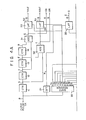
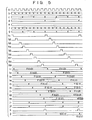
- Figs. 4A and 4B are block diagrams showing the internal circuit of the 3 x 3 filter 2
- Fig. 5 is a timing chart for explaining the mode of operation of the filter 2.
- Reference symbols a to t in Figs. 4A and 4B correspond to waveforms a to l in Fig. 5.
- a signal a is a clock pulse CK and is supplied to a counter 11.
- the counter 11 frequency-divides the clock pulse a to produce an output signal b.
- the signal b is supplied to another counter 12.
- the counter 12 frequency-divides the signal b to obtain an output signal c.
- the signal c is supplied to a further counter 13.
- the counter 13 frequency-divides the signal c to obtain an output signal d.
- the signal d is supplied to a still further counter 14 to be frequency-divided to obtain an output signal e.
- the signals b and d are added by an adder 32 which produces a signal f.
- the signals c and e are added by another adder 31 which produces a signal g.
- the signal f corresponds to the signal X in shown in Fig. 3, while the signal g corresponds to the signal Y in shown in the same figure.
- the signals X in and Y in are signals for sequentially scanning an area of a 3 x 3 matrix having the input pixel as the center. The input pixel is then shifted by one pixel in the x-direction and the corresponding 3 x 3 matrix area is scanned.
- the signals X in and Y in constitute x- and y-addresses for reading out the image data from the OID memory 1.
- the pixel data from the memory 1 is parallel-supplied to latches 41 to 49 as image data F.
- the timings at which the data F is latched in these latches 41 to 49 are determined by control signals h I to h 9 from a shift register 22.
- An output timing from the shift register 22 is synchronous with the clock pulse a.
- Individual image data i.e., F(0,0), F(l, 0), F(0, 1), F (2, 0), F(l, 1) , F (2, 1), F(0, 2), F (1, 2) and F(2, 2) are latched in the latches 41 to 49, respectively, and appear as outputs i l to i 9 .
- the signals i l to i 9 are added by adders 51 to 58.
- Fig. 6 is a block diagram for explaining the linear combination of the original image data and the filtered image data from the 3 x 3 filter.
- the linear combination circuit comprises an address signal generator 9, the multipliers 4 and 5, and the adder device 6.
- a clock pulse a' is supplied to a counter 61 which frequency-divides the pulse a' to produce a signal b'.
- the signal b' is supplied to another counter 62 to be further frequency-divided to produce a signal c'.
- the signals c' and b' (d') are used as x- and y-address signals for accessing the memories 1, 3 and 7 shown in Fig. 1.
- FIG. 6 correspond to the signals a to d in Fig. 1, respectively.
- Readout of the input image data and writing of the processed image data are executed by scanning one line after another from the left to the right of the image shown in Fig. 2B.
- the readout original image data is supplied as a signal g' to one input terminal of a multiplier element 65 of the multiplier 5 and the filtered image data is supplied as a signal j' to one input terminal of a multiplier element-66 of the multiplier 4.
- Registers 64 and 63 of the respective multipliers 4 and 5 store the parameters A and B supplied from the parameter input terminal 8.
- the parameters A and B are produced as signals k and k' in response to shift control signals h' and e' and are supplied to the other input terminal of each of the multiplier elements 66 and 65. Then, the multiplier elements 65 and 66 multiply the respective image data by the corresponding weight coefficients, and output data (m', n') from the multiplier elements 65 and 66 are supplied to an adder 67 to be added together. In this manner, the linear combination is performed, and processed image data p' is obtained.
- the processed image data p' is stored in a predetermined area of the PID memory 7 which is selected by signals X and Y from the address signal generator 9.
- Fig. 7 is a block diagram showing an example of the parameter input terminal 8 shown in Fig. 1.
- the terminal comprises first and second parameter generators 78 and 79.
- variable resistors 71 and 72 are respectively connected between a power supply of +5 V and ground.
- the analog signals obtained from the resistors 71 and 72 are converted into digital signals by A/D converters 73 and 74 and the digital signals are supplied to ALUs 75 and 76, respectively.
- the ALUs 75 and 76 convert the input signals into parameters and produce the parameters A and B.
- the ALUs 75 and 76 perform the calculation according to equation (1) such that the analog signals from the resistors correspond to the coefficients of the linear combination.
- a parameter input terminal 80 as shown in Fig. 8 may be conveniently used, together with an input device such as a digitizer or a light pen device which is capable of designating a single point on the x-y plane.
- parameters A and B are plotted along the two orthogonal axes, that is, the x- and y-axes.
- Fig. 8 shows the frequency characteristics for 16 typical points. As the parameter A increases (to the right from a central point 82), a sharper high-pass filter frequency response curve is obtained.
- the parameter B corresponds to the ratio of the original image data component to the processed image data. As the parameter B increases (upward from the central point 82), the processed image data becomes closer to the original image data. It is to be noted that points other than the 16 points indicated in the figure can be designated. In this manner, by designating a point by its coordinates, the spatial frequency characteristics to be obtained can be visually confirmed by the operator, thus improving the operability of the parameter input terminal.
- a set of parameters can be selected using a parameter input terminal, so that desired spatial frequency characteristics may be designated.
- Various types of characteristics can be finely designated.
- the frequency characteristics to be obtained can be visually confirmed from the values of the parameters.
- a spatial filtering apparatus with improved operability can be provided.
- fine designation can be performed and operability is improved due to easy confirmation of the designated parameters on the x-y plane.
- nine multiplication operations are performed for one image data.
- only two multiplication operations are required, so that high-speed operation can be performed.
- An original image data memory (to be referred to as OID memory) 1 stores original image data to be filtered.
- the original image data in the OID memory 1 is read out and is supplied to a 3 x 3 filter 2.
- the smoothening 3 x 3 filter 2 adds together the data of each given pixel with data of the eight surrounding pixels having a given pixel as its center.
- the filter 2 filters the sum data as the pixel data of the given pixel and the filtered image data from the filter 2 is supplied to and stored in a filtered image data storage memory (to be referred to as FID memory) 3.
- FID memory filtered image data storage memory
- the image data filtered by the 3 x 3 filter 2 and stored in the memory 3 is read out therefrom and is supplied to a multiplier 5.
- the multiplier 5 multiplies the filtered image data by a parameter B set for the original image data.
- the product from the multiplier 5 is supplied to an image data adder device (to be referred to as adder device) 6.
- the adder device 6 also receives the pixel data of the original image data from the memory 1.
- the adder device 6 adds the two input data and supplies the sum data to a processed image data memory (to be referred to as FID memory) 7.
- a parameter B of the multiplier 5 is generated from a parameter input terminal 90 in the following manner. That is, a DC voltage +5 V is divided by a variable resistor 92, and the resultant voltage is supplied to an A/D converter 94 which supplies a digital signal to an ALU 96.
- the ALU 96 calculates the parameter B.
- the image data filtered by the 3 x 3 filter 2 and stored in the memory 3 is read out for each such parameter. Then, the original image data and the filtered image data are subjected to linear combination by the adder device 5. Thus, high-speed processing can be achieved.
- the readout timings from the memories 1 and 3 are synchronized for performing addition of the original image data and the filtered image data for the same pixel, the image data of this pixel is supplied to the adder device 6 and the sum data is supplied to the memory 7. Accordingly, when the contents of the memory 7 are read out and displayed by an image display device, an image in which the original image data and the filtered image.data are weighted by desired coefficients can be displayed.
- Fig. 10 shows the multiplier 5 and the adder device 6 for weighting and adding the original image data and the filtered image data from the 3 x 3 filter.
- a clock pulse a is frequency-divided by a counter 61 which produces a signal b.
- the signal b is supplied to another counter 62 which frequency-divides the signal b and produces a signal c.
- the signals d and c are used as x- and y-address signals for accessing the memories 1, 3 and 7, shown in Fig. 9.
- Readout of the input image data and writing of the processed image data are performed by scanning one line after another from the left toward the right of the image.
- the readout original image data is supplied as g, and filtered image data is supplied as j.
- a register 64 stores a parameter B from the variable resistor 92 shown in Fig. 9.
- a multiplier element 66 calculates the product of the filtered image data and the parameter B, and the obtained product is added to the original image data by an adder 67, thus performing linear combination.
- the obtained result is stored in an address of the memory 7 which is accessed by the x- and y-address signals d and c.
- a single parameter is input by a parameter input means of an extremely simple configuration, e.g., a variable resistor.
- a parameter input means of an extremely simple configuration e.g., a variable resistor.
- flat spatial frequency characteristics equal to the original image
- high-frequency components edge are gradually enhanced.
- the original image data is subjected to spatial frequency processing for variable spatial frequency characteristics.
- the addition ratio of the filtered image data to the original image data can be changed by adjusting the variable resistor 92.
- the ratio of the image data which has been subjected to edge enhancement to the original image data is increased, and images for varying ratios of such image data can be displayed.
- This facilitates diagnosis and allows the formation of various composite images, so that the data of the image can be freely reproduced in a desired manner.
- the original image data and the filtered image data are stored in separate memories and are weighted separately by desired weight coefficients, a complex operation need not be performed. High-speed operation can be performed, and desired composite images can be obtained within a short period of time, thereby facilitating easy diagnosis.
- a 3 x 3 filter is used for smoothing the image data.
- the present invention is not limited to this.
- a series of processing steps such as filtering, weighting and addition can be replaced by software to be executed by a computer.
- the 3 x 3 filter 2 has a smoothening function.
- a filter having an edge enhancing function can be used.
Landscapes
- Physics & Mathematics (AREA)
- General Physics & Mathematics (AREA)
- Engineering & Computer Science (AREA)
- Theoretical Computer Science (AREA)
- Image Processing (AREA)
- Facsimile Image Signal Circuits (AREA)
Applications Claiming Priority (4)
| Application Number | Priority Date | Filing Date | Title |
|---|---|---|---|
| JP57176700A JPS5966272A (ja) | 1982-10-07 | 1982-10-07 | 空間フイルタリング装置 |
| JP176700/82 | 1982-10-07 | ||
| JP233565/82 | 1982-12-28 | ||
| JP23356582A JPS59123068A (ja) | 1982-12-28 | 1982-12-28 | 画像表示処理装置 |
Publications (4)
| Publication Number | Publication Date |
|---|---|
| EP0106265A2 true EP0106265A2 (fr) | 1984-04-25 |
| EP0106265A3 EP0106265A3 (en) | 1985-03-20 |
| EP0106265B1 EP0106265B1 (fr) | 1989-01-11 |
| EP0106265B2 EP0106265B2 (fr) | 1992-08-26 |
Family
ID=26497511
Family Applications (1)
| Application Number | Title | Priority Date | Filing Date |
|---|---|---|---|
| EP83109915A Expired EP0106265B2 (fr) | 1982-10-07 | 1983-10-04 | Appareil de traitement de données d'image |
Country Status (3)
| Country | Link |
|---|---|
| US (1) | US4590582A (fr) |
| EP (1) | EP0106265B2 (fr) |
| DE (1) | DE3378933D1 (fr) |
Cited By (1)
| Publication number | Priority date | Publication date | Assignee | Title |
|---|---|---|---|---|
| FR2653961A1 (fr) * | 1989-11-02 | 1991-05-03 | Gen Electric Cgr | Procede de traitement d'une image pour en ameliorer les contrastes. |
Families Citing this family (27)
| Publication number | Priority date | Publication date | Assignee | Title |
|---|---|---|---|---|
| IL71878A (en) * | 1984-05-21 | 1987-11-30 | Elscint Ltd | Intensity level windowing system for image displays |
| US4745567A (en) * | 1985-02-01 | 1988-05-17 | American Telephone And Telegraph Company At&T Bell Laboratories | Moment generator |
| US4777620A (en) * | 1985-02-20 | 1988-10-11 | Elscint Ltd. | Data compression system |
| US4769778A (en) * | 1985-02-25 | 1988-09-06 | Siemens Aktiengesellschaft | Circuit arrangement comprising a matrix-shaped memory arrangement for digital filtration of image signals in row and column directions |
| US4753246A (en) * | 1986-03-28 | 1988-06-28 | The Regents Of The University Of California | EEG spatial filter and method |
| US4761819A (en) * | 1987-02-27 | 1988-08-02 | Picker International, Inc. | Adaptive noise reduction filter for reconstructed images |
| US5051902A (en) * | 1987-10-20 | 1991-09-24 | Fuji Photo Film Co., Ltd. | Method and apparatus for radiation image processing and x-ray image processing, including spatial frequency filtering to improve graininess |
| US5086477A (en) * | 1990-08-07 | 1992-02-04 | Northwest Technology Corp. | Automated system for extracting design and layout information from an integrated circuit |
| US5172419A (en) * | 1991-03-05 | 1992-12-15 | Lumisys, Inc. | Medical image processing system |
| US5636327A (en) * | 1991-09-18 | 1997-06-03 | Matsushita Electric Industrial Co., Ltd. | Neural network circuit |
| US5311428A (en) * | 1992-06-05 | 1994-05-10 | Summit World Trade Corporation | Real time filter for data processing |
| EP0731951B1 (fr) * | 1993-02-26 | 2000-07-05 | E-Y Laboratories, Inc. | Procede et systeme d'analyse optique d'echantillons |
| US5440647A (en) * | 1993-04-22 | 1995-08-08 | Duke University | X-ray procedure for removing scattered radiation and enhancing signal-to-noise ratio (SNR) |
| US5857038A (en) * | 1993-06-29 | 1999-01-05 | Canon Kabushiki Kaisha | Image processing apparatus and method for synthesizing first and second image data |
| US5595179A (en) * | 1995-05-02 | 1997-01-21 | Acuson Corporation | Adaptive persistence processing |
| US5872602A (en) * | 1995-12-13 | 1999-02-16 | Johnson; Robert E. | Fluoroscopic imaging system with image enhancement apparatus and method |
| US5708690A (en) * | 1996-10-11 | 1998-01-13 | General Electric Company | Methods and apparatus for helical image reconstruction in a computed tomography fluoro system |
| US6246783B1 (en) | 1997-09-17 | 2001-06-12 | General Electric Company | Iterative filter framework for medical images |
| WO1999040536A1 (fr) * | 1998-02-10 | 1999-08-12 | Ey Laboratories, Inc. | Systeme de reflectometrie avec compensation pour topologie de supports d'echantillons et avec elimination synchrone du bruit de reseau |
| US6424730B1 (en) * | 1998-11-03 | 2002-07-23 | Eastman Kodak Company | Medical image enhancement method for hardcopy prints |
| US6778692B1 (en) * | 2000-08-11 | 2004-08-17 | General Electric Company | Image processing method and apparatus including image improving circuit |
| EP1225756A1 (fr) * | 2001-01-03 | 2002-07-24 | Synoptics Limited | Procédé d'obtention d'une image |
| DE10143484A1 (de) * | 2001-09-05 | 2003-04-03 | Siemens Ag | Adaptives Filter |
| JP4724124B2 (ja) * | 2004-10-08 | 2011-07-13 | パナソニック株式会社 | 画像処理装置および画像処理プログラム |
| US8014034B2 (en) * | 2005-04-13 | 2011-09-06 | Acd Systems International Inc. | Image contrast enhancement |
| GB2438660B (en) * | 2006-06-02 | 2011-03-30 | Tandberg Television Asa | Recursive filter system for a video signal |
| US8189050B1 (en) | 2006-07-19 | 2012-05-29 | Flir Systems, Inc. | Filtering systems and methods for infrared image processing |
Family Cites Families (6)
| Publication number | Priority date | Publication date | Assignee | Title |
|---|---|---|---|---|
| JPS5458393A (en) * | 1977-10-19 | 1979-05-11 | Hitachi Medical Corp | Radiant ray revolving sectional layer device |
| NL7800406A (nl) * | 1978-01-13 | 1979-07-17 | Philips Nv | Inrichting voor het filteren van gecomprimeerde pulscode gemoduleerde signalen. |
| NL184298C (nl) * | 1979-07-19 | 1989-06-01 | Philips Nv | Inrichting voor verschilbeeldbepaling. |
| US4335307A (en) * | 1980-04-21 | 1982-06-15 | Technicare Corporation | Radiographic apparatus and method with automatic exposure control |
| DE3149483A1 (de) * | 1981-12-14 | 1983-06-23 | Siemens AG, 1000 Berlin und 8000 München | Roentgendiagnostikeinrichtung zur erstellung von subtraktionsbildern |
| NL8202417A (nl) * | 1982-06-15 | 1984-01-02 | Philips Nv | Inrichting en werkwijze voor het verwerken van roentgenbeelden. |
-
1983
- 1983-10-04 DE DE8383109915T patent/DE3378933D1/de not_active Expired
- 1983-10-04 EP EP83109915A patent/EP0106265B2/fr not_active Expired
- 1983-10-06 US US06/539,401 patent/US4590582A/en not_active Expired - Fee Related
Cited By (1)
| Publication number | Priority date | Publication date | Assignee | Title |
|---|---|---|---|---|
| FR2653961A1 (fr) * | 1989-11-02 | 1991-05-03 | Gen Electric Cgr | Procede de traitement d'une image pour en ameliorer les contrastes. |
Also Published As
| Publication number | Publication date |
|---|---|
| EP0106265B2 (fr) | 1992-08-26 |
| DE3378933D1 (en) | 1989-02-16 |
| EP0106265A3 (en) | 1985-03-20 |
| EP0106265B1 (fr) | 1989-01-11 |
| US4590582A (en) | 1986-05-20 |
Similar Documents
| Publication | Publication Date | Title |
|---|---|---|
| US4590582A (en) | Image data processing apparatus for performing spatial filtering of image data | |
| EP0112582B1 (fr) | Dispositif de visualisation d'images superposées | |
| US4831447A (en) | Method and apparatus for anti-aliasing an image boundary during video special effects | |
| JP2612939B2 (ja) | イメージ表示システム用補間装置およびイメージ表示システム | |
| US6493467B1 (en) | Image processor, data processor, and their methods | |
| EP0407213B1 (fr) | Appareil de traitement d'image | |
| EP0513516A2 (fr) | Procédé et appareil pour la réduction d'images numériques | |
| US5202670A (en) | Image processing apparatus | |
| JPS5814270A (ja) | 画像走査記録方法 | |
| CA2285088A1 (fr) | Dispositif et procedes servant a brouiller de facon selective l'image cache d'une image composite | |
| US4682301A (en) | Digital filter for processing two-dimensional digital image | |
| JPH022594A (ja) | 二次元カラーディスプレイ発生装置 | |
| US5438654A (en) | System and method for sharpening texture imagery in computer generated interactive graphics | |
| US5930407A (en) | System and method for efficiently generating cubic coefficients in a computer graphics system | |
| JP2975691B2 (ja) | 離散コサイン変換を用いる画像のサンプルレート変換のシステムおよび方法 | |
| JP3298732B2 (ja) | 放射線画像の部分の表示方法 | |
| US6222173B1 (en) | Image sharpening and re-sampling method | |
| EP0908845B1 (fr) | Procédé d'accentuation et de re-échantillonage d'image | |
| EP0584941A1 (fr) | Méthodes et appareils pour générer des motifs graphiques | |
| EP0511606B1 (fr) | Interpolateur parallèle pour agrandissement d'image numérique à grande vitesse | |
| US6714210B1 (en) | Continuous kernel image interpolation | |
| US5506693A (en) | Addressing mechanism for interfacing spatially defined imagery data with sequential memory | |
| US6414682B1 (en) | System and method for transitioning between two filters, allowing for the use of higher order interpolation | |
| Lippman | The graphic-photographic computer: aspects of interpolation | |
| Sivaswamy et al. | A real-time implementation of nonlinear unsharp masking with FPLDs |
Legal Events
| Date | Code | Title | Description |
|---|---|---|---|
| PUAI | Public reference made under article 153(3) epc to a published international application that has entered the european phase |
Free format text: ORIGINAL CODE: 0009012 |
|
| 17P | Request for examination filed |
Effective date: 19831028 |
|
| AK | Designated contracting states |
Designated state(s): DE FR GB NL |
|
| RAP1 | Party data changed (applicant data changed or rights of an application transferred) |
Owner name: KABUSHIKI KAISHA TOSHIBA |
|
| PUAL | Search report despatched |
Free format text: ORIGINAL CODE: 0009013 |
|
| AK | Designated contracting states |
Designated state(s): DE FR GB NL |
|
| 17Q | First examination report despatched |
Effective date: 19860128 |
|
| R17C | First examination report despatched (corrected) |
Effective date: 19860811 |
|
| GRAA | (expected) grant |
Free format text: ORIGINAL CODE: 0009210 |
|
| AK | Designated contracting states |
Kind code of ref document: B1 Designated state(s): DE FR GB NL |
|
| REF | Corresponds to: |
Ref document number: 3378933 Country of ref document: DE Date of ref document: 19890216 |
|
| ET | Fr: translation filed | ||
| PLBI | Opposition filed |
Free format text: ORIGINAL CODE: 0009260 |
|
| 26 | Opposition filed |
Opponent name: LINOTYPE AG Effective date: 19891010 |
|
| NLR1 | Nl: opposition has been filed with the epo |
Opponent name: LINOTYPE AG |
|
| PGFP | Annual fee paid to national office [announced via postgrant information from national office to epo] |
Ref country code: GB Payment date: 19910920 Year of fee payment: 9 |
|
| PGFP | Annual fee paid to national office [announced via postgrant information from national office to epo] |
Ref country code: FR Payment date: 19911007 Year of fee payment: 9 |
|
| PGFP | Annual fee paid to national office [announced via postgrant information from national office to epo] |
Ref country code: NL Payment date: 19911031 Year of fee payment: 9 Ref country code: DE Payment date: 19911031 Year of fee payment: 9 |
|
| PUAH | Patent maintained in amended form |
Free format text: ORIGINAL CODE: 0009272 |
|
| STAA | Information on the status of an ep patent application or granted ep patent |
Free format text: STATUS: PATENT MAINTAINED AS AMENDED |
|
| 27A | Patent maintained in amended form |
Effective date: 19920826 |
|
| AK | Designated contracting states |
Kind code of ref document: B2 Designated state(s): DE FR GB NL |
|
| NLR4 | Nl: receipt of corrected translation in the netherlands language at the initiative of the proprietor of the patent | ||
| PG25 | Lapsed in a contracting state [announced via postgrant information from national office to epo] |
Ref country code: GB Effective date: 19921004 |
|
| NLR2 | Nl: decision of opposition | ||
| ET3 | Fr: translation filed ** decision concerning opposition | ||
| NLR3 | Nl: receipt of modified translations in the netherlands language after an opposition procedure | ||
| PG25 | Lapsed in a contracting state [announced via postgrant information from national office to epo] |
Ref country code: NL Effective date: 19930501 |
|
| GBPC | Gb: european patent ceased through non-payment of renewal fee |
Effective date: 19921004 |
|
| NLV4 | Nl: lapsed or anulled due to non-payment of the annual fee | ||
| PG25 | Lapsed in a contracting state [announced via postgrant information from national office to epo] |
Ref country code: FR Effective date: 19930630 |
|
| PG25 | Lapsed in a contracting state [announced via postgrant information from national office to epo] |
Ref country code: DE Effective date: 19930701 |
|
| REG | Reference to a national code |
Ref country code: FR Ref legal event code: ST |